

Page 1
NTE7004
Integrated Circuit
Electronic Channel Select System Control
Description:
The NTE7004 contains CPU/PLL–excluded peripheral circuits such as band switch, +5V power supply (with RST
system use.
Functions:
D Band Switch (2–Input, 4–Output)
D Video Signal, Flyback Pulse, AFT Output–Used Detection of Tuning Mode and Horizontal
Sync Mode
D +5V Power Supply, with RST
D OP Amp for Low–Pass Filter (for Frequency Synthesizer)
Features:
D The Band Switch Truth Table can be changed in a short period of time at the user’s option.
D The Band Switch is of PNP output type which need not be driven externally.
D The OP Amp for Low–Pass Filter is excellant in pulse response because of it’s High–Imped-
ance Input Pin.
), sync detector, low–pass filter for color TV/VCR frequency synthesizer channel select
Output (for CPU)
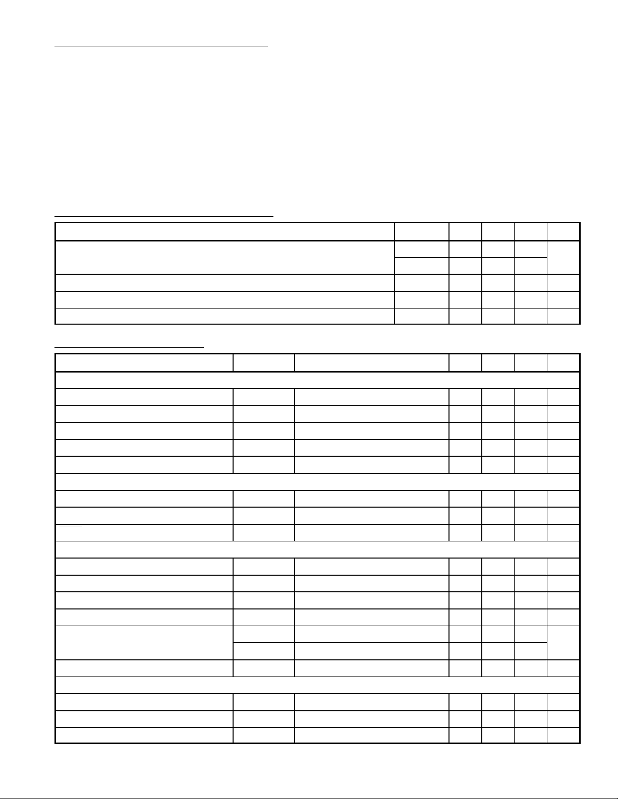
Absolute Maximum Ratings:
Allowable Power Dissipation (T
Operating Temperature Range, T
Storage Temperature Range, T
(TA = +25°C unless otherwise specified)
≤ +65°C), P
A
opr
stg
Band Switch Section
V
Maximum Supply Voltage, V
CC1
Maximum Load Current, I
, I15, I16, I
14
13max
17max
Maximum Applied Voltage (Output OFF), V
Maximum Applied Voltage (Input, V
= 14V), V
cc
+5V Power Supply Section
V
Maximum Supply Voltage, V
CC2
+5V Output Current, I
8max
10max
dmax
, V15, V16, V
14
, V
6max
7ma
17max
770mW. . . . . . . . . . . . . . . . . . . . . . . . . . . . . . . . . . .
–20° to +65°C. . . . . . . . . . . . . . . . . . . . . . . . . . . . . . . . . . . . . . . . .
–55° to +125°C. . . . . . . . . . . . . . . . . . . . . . . . . . . . . . . . . . . . . . . . . .
15V. . . . . . . . . . . . . . . . . . . . . . . . . . . . . . . . . . . . . . . . . . . . . . .
–50mA. . . . . . . . . . . . . . . . . . . . . . . . . . . . . . . . . . . . . . . . .
–15V. . . . . . . . . . . . . . . . . . . . . . . . . .
12V. . . . . . . . . . . . . . . . . . . . . . . . . . . . . . .
15V. . . . . . . . . . . . . . . . . . . . . . . . . . . . . . . . . . . . . . . . . . . . . . .
–38mA. . . . . . . . . . . . . . . . . . . . . . . . . . . . . . . . . . . . . . . . . . . . . . . . . . . . . . . .
Page 2
Absolute Maximum Ratings (Cont’d): (TA = +25°C unless otherwise specified)
Tuning Detector Section
Maximum Input Voltage, V
Maximum Input Voltage, V
Maximum Input Voltage (Negative Polarity), –V
Maximum Comparator Difference Voltage, V
Maximum Output Current, I
2max
3max
1max
19
2max
– V
20
Low–Pass Filter Section
Maximum Applied Voltage, V
Maximum Input Voltage, V
12max
11max
Recommended Operating Conditions: (TA = +25°C unless otherwise specified)
Parameter Symbol Min Typ Max Unit
V
CC1
–1.4V. . . . . . . . . . . . . . . . . . . . . . . . . . . . . . . . . . .
–3mA. . . . . . . . . . . . . . . . . . . . . . . . . . . . . . . . . . . . . . . . . . . . . . . . . . . .
3.5V. . . . . . . . . . . . . . . . . . . . . . . . . . . . . . . . . . . . . . . . . . . . . . . . . . . . . .
V. . . . . . . . . . . . . . . . . . . . . . . . . . . . . . . . . . . . . . . . . . . . . . . . . . . . .
6V. . . . . . . . . . . . . . . . . . . . . . . . . . . . . . . . . . . . .
35V. . . . . . . . . . . . . . . . . . . . . . . . . . . . . . . . . . . . . . . . . . . . . . . . . . . .
5.9V. . . . . . . . . . . . . . . . . . . . . . . . . . . . . . . . . . . . . . . . . . . . . . . . . . . . .
Supply Voltage Range (V
) V
CC1
(V
) V
CC2
Output Current (Tuning Detection Section) I4, I
Load Current (LPF Section) I
Comparator Voltage Setting Range (Tuning Detector Section) V
Electrical Characteristics: (TA = +25°C, V
= 12V, V
CC1
= 12V unless otherwise specified)
CC2
Parameter Symbol Test Conditions Min Typ Max Unit
Band Switch Section
Quiescent Current Dissipation I
Output Saturation Voltage F
Input “H” Level Voltage V
Input “L” Level Voltage V
Output Leakage Current I
CC1
1 to 4 satIO =
, V
6TH
7TH
, V
6TL
7TL
FL
–40mA 0 – 0.7 V
–15V – – –50 µA
+5V Power Supply Section
Quiescent Current Dissipation I
+5V Output Voltage V
RST Output Voltage V
CC2
8
9sat
I8 = –30mA 4.5 – 5.5 V
I9 = –100µA 4.5 – 5.5 V
Tuning Detection Section
Input Threshold Voltage V
Comparator Voltage V
Window Comparator “H” Voltage V
Window Comparator “L” Voltage V
Output Saturation Voltage V
Low–Pass Filter Output Current I
V
2TH
C19
CH
CL
4sat
5sat
OL
I
= 2mA 0 0.33 0.7 V
sink
I
= 2mA 0 0.33 0.7
sink
LPF Section
Output Saturation Voltage V
Input Threshold Voltage V
Input Current I
12sat
11TH
11
12
10
13
19
9.0 12.0 14.0 V
9.0 12.0 14.0
5
– – 3 mA
– 3 5 mA
2.7 – 7.0 V
– 16.0 – mA
2.2 – – V
0 – 0.8 V
– 3.6 – mA
0.4 0.72 1.5 V
3.7 4.0 4.3 V
5.7 6.0 6.3 V
2.7 3.0 3.3 V
–1.8 – –0.9 mA
0 – 0.3 V
2.0 – 2.4 V
– – 20 nA
Page 3

Band Switch Truth Table
Input Output
A B F
1
F
2
F
3
(Pin7) (Pin6) (Pin14) (Pin15) (Pin16) (Pin17)
L L H Z Z Z
H L Z H Z Z
L H Z Z H Z
H H Z Z Z H
Z: High Impedance
Operation of Tuning Detection Section
Tuning Mode LPF Output AFT OUT1 OUT2
AFT–L L L
F
4
Unsynchronized L
Synchronized H
AFT–L: V
AFT–C: VCL < V
AFT–H: V
< V
AFT
AFT
Sync Separator
> V
CL
< V
AFT
CH
Output 1
CH
Pin Connection Diagram
1
FBP
AFT
2
3
4
AFT–C L L
AFT–H L L
AFT–L H L
AFT–C H H
AFT–H L H
LPF
20
19
OP Amp Input
18
GND
17
Bandswitch Output F4
Bandswitch Input B
Bandswitch Input A
+ 5V Output
Output
RST
V
CC
5Output 2
6
7
8
9
2
10 11
16
Bandswitch Output F3
15
Bandswitch Output F2
14
Bandswitch Output F1
VCC 1
13
12
Output to TV
PLL Input
Page 4

20 11
.280 (7.12) Max
110
.995 (25.3) Max
.280
(7.12)
.100 (2.54) .125 (3.17) Min .385 (9.8)
.300 (7.62)
 Loading...