

Page 1
NTE7000
Integrated Circuit
5W Audio Amplifier with Muting
Description:
The NTE7000 is a monolithic integrated circuit in a 16–Lead DIP type package intended for use
as a low frequency power amplifier in a wide range of applications in radio and TV sets.
Features:
D Muting Facility
D Protection Against Chip Over Temperature
D Very Low Noise
D High Supply Voltage Rejection
D Low “Switch–On” Noise
D Voltage Range: 4V to 30V
Absolute Maximum Ratings:
Supply Voltage, VS 30V. . . . . . . . . . . . . . . . . . . . . . . . . . . . . . . . . . . . . . . . . . . . . . . . . . . . . . . . . . . . . . . . .
Output Peak Current, I
Non–Repetitive 3A. . . . . . . . . . . . . . . . . . . . . . . . . . . . . . . . . . . . . . . . . . . . . . . . . . . . . . . . . . . . . . .
Repetitive 2.5A. . . . . . . . . . . . . . . . . . . . . . . . . . . . . . . . . . . . . . . . . . . . . . . . . . . . . . . . . . . . . . . . . .
Input Voltage, V
0 to +V
I
Differential Input Voltage, V
Muting Threshold Voltage, V
Power Dissipation, P
TA = +80°C 1W. . . . . . . . . . . . . . . . . . . . . . . . . . . . . . . . . . . . . . . . . . . . . . . . . . . . . . . . . . . . . . . . . .
T
= +60°C 6W. . . . . . . . . . . . . . . . . . . . . . . . . . . . . . . . . . . . . . . . . . . . . . . . . . . . . . . . . . . . . . . . . .
C
Junction Temperature Range, T
Storage Temperature Range, T
tot
O
±7V. . . . . . . . . . . . . . . . . . . . . . . . . . . . . . . . . . . . . . . . . . . . . . . . . . . . . . . . .
I
11
–40° to +150°C. . . . . . . . . . . . . . . . . . . . . . . . . . . . . . . . . . . . . . . . . . .
j
–40° to +150°C. . . . . . . . . . . . . . . . . . . . . . . . . . . . . . . . . . . . . . . . . .
stg
VS V. . . . . . . . . . . . . . . . . . . . . . . . . . . . . . . . . . . . . . . . . . . . . . . . . . . . . .
V. . . . . . . . . . . . . . . . . . . . . . . . . . . . . . . . . . . . . . . . . . . . . . . . . . . . . . . . . . . . .
S
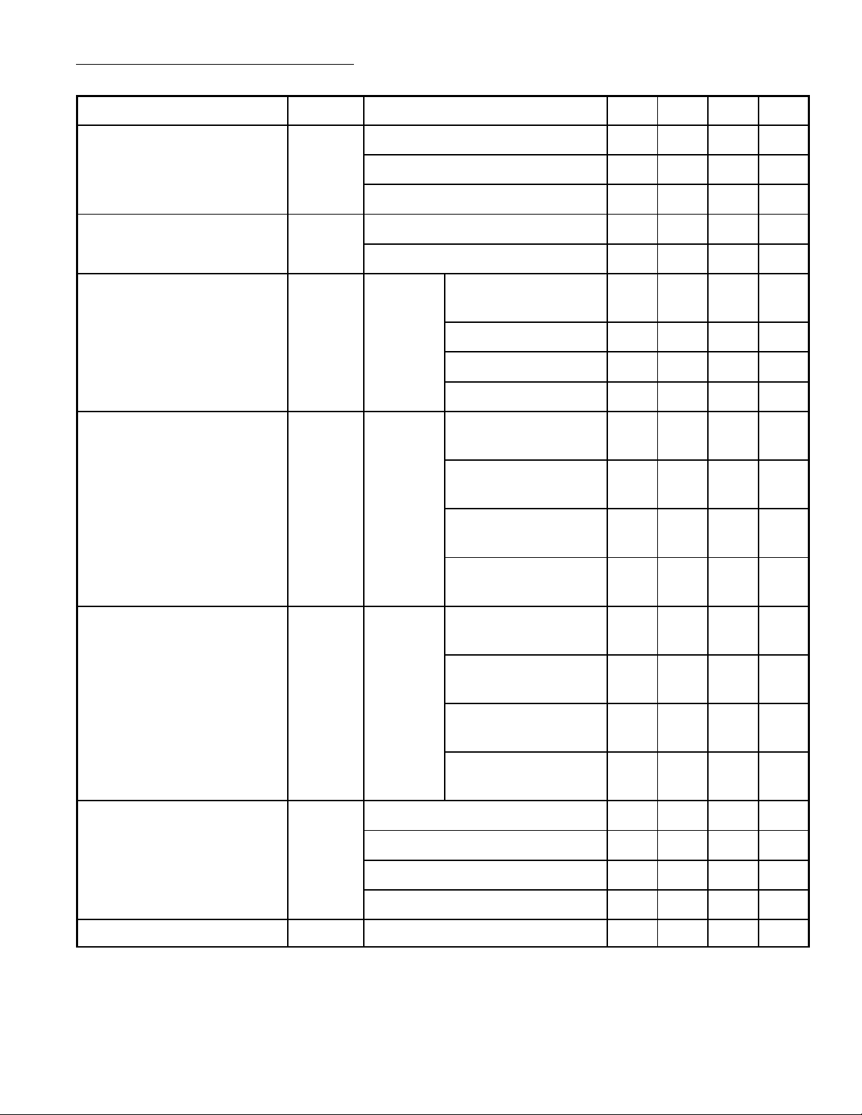
Electrical Characteristics:
Parameter
(TA = +25°C, Rth(heatsink) = 20°C/W, unless otherwise specified)
Symbol Test Conditions Min Typ Max Unit
Supply Voltage V
Quiescent Output Voltage V
S
O
VS = 4V 1.6 2.1 2.5 V
4 – 30 V
VS = 14V 6.7 7.2 7.8 V
VS = 30V 14.4 15.5 16.8 V
Page 2
Electrical Characteristics (Cont’d): (TA = +25°C, Rth(heatsink) = 20°C/W, unless otherwise
specified)
Parameter
Quiescent Drain Current I
Symbol Test Conditions Min Typ Max Unit
d
Vs = 4V – 15 – mA
VS = 14V – 17 – mA
VS = 30V – 21 35 mA
Output Stage Saturation V
CEsat
IC = 1A – 0.5 – V
V oltage
IC = 2A – 1 – V
Output Power P
O
d = 10%,
f = 1kHz
Harmonic Distortion d f = 1kHz
VS = 9V, RL = 4Ω ,
2.2 2.5 – W
Note 1
VS = 14V, RL = 4Ω 5 5.5 – W
VS = 18V, RL = 8Ω 5 5.5 – W
VS = 24V, RL = 16Ω 4.5 5.3 – W
VS = 9V, RL = 4Ω,
P
= 50mW to 1.5W
O
VS = 14V, RL = 4Ω,
P
= 50mW to 3W
O
– 0.1 – %
– 0.1 – %
Input Sensitivity V
Input Saturation Voltage V
(rms)
VS = 18V, RL = 8Ω,
P
= 50mW to 3W
O
VS = 24V, RL = 16Ω,
P
= 50mW to 3W
O
i
f = 1kHz
VS=9V, RL=4Ω,
P
=2.5W
O
VS=14V, RL=4Ω,
P
=5.5W
O
VS=18V, RL=8Ω,
P
=5.5W
O
VS=24V, RL=16Ω,
P
=5.3W
O
VS = 9V 0.8 – – V
i
– 0.1 – %
– 0.1 – %
– 37 – mV
– 49 – mV
– 73 – mV
– 100 – mV
VS = 14V 1.3 – – V
VS = 18V 1.8 – – V
VS = 24V 2.4 – – V
Input Resistance (Pin8) R
f = 1kHz 60 100 – KΩ
i
Note 1. With an external resistor of 100Ω between Pin3 and +VS.
Page 3

Electrical Characteristics (Cont’d): (TA = +25°C, Rth(heatsink) = 20°C/W, unless otherwise
specified)
Parameter
Drain Current I
Symbol Test Conditions Min Typ Max Unit
d
f = 1kHz
Efficiency η f = 1kHz
VS=9V, RL=4Ω,
P
=2.5W
O
VS=14V, RL=4Ω,
P
=5.6W
O
VS=18V, RL=8Ω,
P
=5.5W
O
VS=24V, RL=16Ω,
P
=5.3W
O
VS=9V, RL=4Ω,
P
=2.5W
O
VS=14V, RL=4Ω,
P
=5.5W
O
VS=18V, RL=8Ω,
P
=5.6W
O
VS=24V, RL=16Ω,
P
=5.3W
O
– 380 – mA
– 550 – mA
– 410 – mA
– 295 – mA
– 73 – %
– 71 – %
– 74 – %
– 75 – %
Small Signal Bandwidth
BW VS = 14V, RL = 4Ω, PO = 1W 40 to 40,000 Hz
(–3dB)
Voltage Gain (Open Loop) G
Vo ltage Gain
G
V
V
(Closed Loop)
Total Noise Input e
N
Signal to Noise Ratio S/N
VS = 14V, f = 1kHz – 75 – dB
VS = 14V, RL = 4Ω, f = 1kHz,
P
= 1W
O
39.5 40.0 40.5 dB
Rg = 50Ω – 1.2 – µV
Rg = 1kΩ – 1.3 –
Rg = 10kΩ – 1.5 4.0
Note 2
Rg = 50Ω – 2.0 –
Rg = 1kΩ – 2.0 –
Rg = 10kΩ – 2.2 5.0
VS = 14V,
Rg = 10kΩ – 90 – dB
PO =
5.5W ,
5.5W ,
R
= 4Ω
L
Rg = 0 – 92 –
Rg = 10kΩ, Note 2 – 87 –
Rg = 0, Note 2 – 87 –
Supply Voltage Rejection SVR VS = 18V, RL = 8Ω, RG = 10kΩ,
f
Thermal Shut–Down
= 100Hz, V
ripple
T
sd
P
= 2.5W – 115 – °C
tot
ripple
= 0.5V
Case Temperature
Note 2. Filter with noise bandwidth: 22Hz to 22kHz.
40 50 – dB
rms
Page 4

Muting Function:
Parameter Symbol Test Conditions Min Typ Max Unit
Muting–Off Threshold
V
T(OFF)
Vo ltage (Pin4)
Muting–On Threshold V
T(ON)
Vo ltage (Pin4)
Input Resistance (Pin5) R
Input Resistance (Pin4) R
Muting Attenuation A
Bootstrap
Threshold
Muting Off 80 200 – kΩ
5
Muting On – 10 30 Ω
4
T
Output
Rg + R1 = 10kΩ 50 60 – dB
Pin Connection Diagram
1
2
V
S
3
4
5Muting
6Inverting Input
16
GND
GND
15
14
GND
13
GND
12 GND
11 GND
1.9 – 4.7 V
0 – 1.3 V
6.2 – V
S
150 – – kΩ
.245
(6.22)
Min
7SVR
8Non–Inverting Input 9 GND
16 9
18
.785 (19.9)
Max
10 GND
.260 (6.6) Max
.300
(7.62)
.200 (5.08)
Max
.100 (2.54)
.700 (17.7)
 Loading...