

Page 1
NTE6885 thru NTE6888
Integrated Circuit
Hex 3–State Buffer/Inverter
Description:
The NTE6885 thru NTE6888 series of devices combines three features usually found desirable in
bus–oriented systems: 1) High impedance logic inputs insure that these devices do not seriously load
the bus; 2) Three–state logic configuration allows buffers not being utilized to be effectively removed
from the bus; 3) Schottky technology allows high–speed operation.
While the NTE6885 to NTE6888 are all buffers, the devices differ in that the NTE6885 (non–inverting)
and the NTE6886 (inverting) provide a two–input Enable which controls all six buffers, while the
NTE6887 (non–inverting) and the NTE6888 (inverting) provide two Enable inputs; one controlling
four buffers and the other controlling the remaining two buffers.
These units are well–suited for Address buffers on the M6800 or similar microprocessor application.
Features:
D High Speed: 8.0ns (Typ)
D Three–State Logic Configuration
D Single +5V Power Supply Requirement
D Compatible with 74LS Logic or 6800 Microprocessor Systems
D High Impedance PNP Inputs Assure Minimal Loading of the Bus
Absolute Maximum Ratings: (TA = +25°C unless otherwise specified for ALL devices)
Power Supply Voltage, VCO 8.0V. . . . . . . . . . . . . . . . . . . . . . . . . . . . . . . . . . . . . . . . . . . . . . . . . . . . . . . .
Input Voltage, VI 5.5V. . . . . . . . . . . . . . . . . . . . . . . . . . . . . . . . . . . . . . . . . . . . . . . . . . . . . . . . . . . . . . . . . .
Operating Ambient Temperature Range, TA 0 to +75°C. . . . . . . . . . . . . . . . . . . . . . . . . . . . . . . . . . . . .
Storage Temperature Range, T
stg
–55° to +150°C. . . . . . . . . . . . . . . . . . . . . . . . . . . . . . . . . . . . . . . . . .
Operating Junction Temperature, T
J
+150°C. . . . . . . . . . . . . . . . . . . . . . . . . . . . . . . . . . . . . . . . . . . . . . .
Electrical Characteristics: (0°C ≤ TA ≤ 75°C and 4.75V ≤ VCC ≤ 5.25V unless otherwise specified
for ALL devices)
Parameter Symbol Test Conditions Min Typ Max Unit
Input Voltage – High Logic State V
IH
VCC = 4.75V, TA = +25°C 2.0 – – V
Input Voltage – Low Logic State V
IL
VCC = 4.75V, TA = +25°C – – 0.8 V
Input Current – High Logic State I
IH
VCC = 5.25V, VIH = 2.4V – – 40 µA
Input Current – Low Logic State I
IL
VCC = 5.25V, VIL = 0.5V, V
IL(E)
= 0.5V – – –400 µA
Input Current – High Impedance State I
IH(E)
VCC = 5.25V, V
IL(I)
= 0.5V, V
IH(E)
= 2V – – –40 µA
Page 2
Electrical Characteristics (Cont’d): (0°C ≤ TA ≤ 75°C and 4.75V ≤ VCC ≤ 5.25V unless otherwise
specified for ALL devices)
Parameter Symbol Test Conditions Min Typ Max Unit
Output Voltage – High Logic State V
OH
VCC = 4.75V, IOH = –5.2mA 2.4 – – V
Output Voltage – Low Logic State V
OL
IOL = 48mA – – 0.5 V
Output Current – High Impedance State I
OZ
VCC = 5.25V, VOH = 2.4V – – 40 µA
VCC = 5.25V, VOH = 0.5V – – –40 µA
Output Short–Circuit Current I
OS
VCC = 5.25V, VO = 0, Note 1 –40 –80 –115 mA
Power Supply Current
NTE6885, NTE6887
NTE6886, NTE6888
I
CC
VCC = 5.25V
–
–
655998
89
mA
Input Clamp Voltage V
IC
VCC = 4.75V, IIC = –12mA – – –1.5 V
Output VCC Clamp Voltage V
OC
VCC = 0, IOC = 12mA – – 1.5 V
Output GND Clamp Voltage V
OC
VCC = 0, IOC = –12mA – – –1.5 V
Input Voltage V
I
II = 1mA 5.5 – – V
Note 1. Only one output can be shorted at a time.
Switching Characteristics: (VCC = 5V, TA = +25°C unless otherwise specified)
NTE6885, NTE6887 NTE6886, NTE6888
Parameter Symbol Test Conditions Min Typ Max Min Typ Max Unit
Propagation Delay Time
t
PHL
CL = 50pF 3 – 12 4 – 11 ns
High to Low State
CL = 250pF – 16 – – 15 – ns
CL = 375pF – 20 – – 18 – ns
CL = 500pF – 23 – – 22 – ns
Propagation Delay Time
t
PLH
CL = 50pF 3 – 13 3 – 10 ns
Low to High State
CL = 250pF – 25 – – 22 – ns
CL = 375pF – 33 – – 28 – ns
CL = 500pF – 42 – – 35 – ns
Transition Time High to Low State
t
THL
CL = 250pF – 10 – – 10 – ns
CL = 375pF – 11 – – 13 – ns
CL = 500pF – 14 – – 15 – ns
Transition Time Low to High State
t
TLH
CL = 250pF – 32 – – 28 – ns
CL = 375pF – 42 – – 38 – ns
CL = 500pF – 60 – – 53 – ns
Propagation Delay Time
High State to Third State
t
PHZ(E)CL
= 5pF – – 10 – – 10 ns
Propagation Delay Time
Low State to Third State
t
PLZ(E)CL
= 5pF – – 12 – – 16 ns
Propagation Delay Time
Third State to High State
t
PZH(E)CL
= 50pF – – 25 – – 22 ns
Propagation Delay Time
Third State to Low State
t
PZL(E)CL
= 50pF – – 25 – – 24 ns
Page 3
Enable 2
V
CC
Enable 4
Enable 2
V
CC
Enable 1
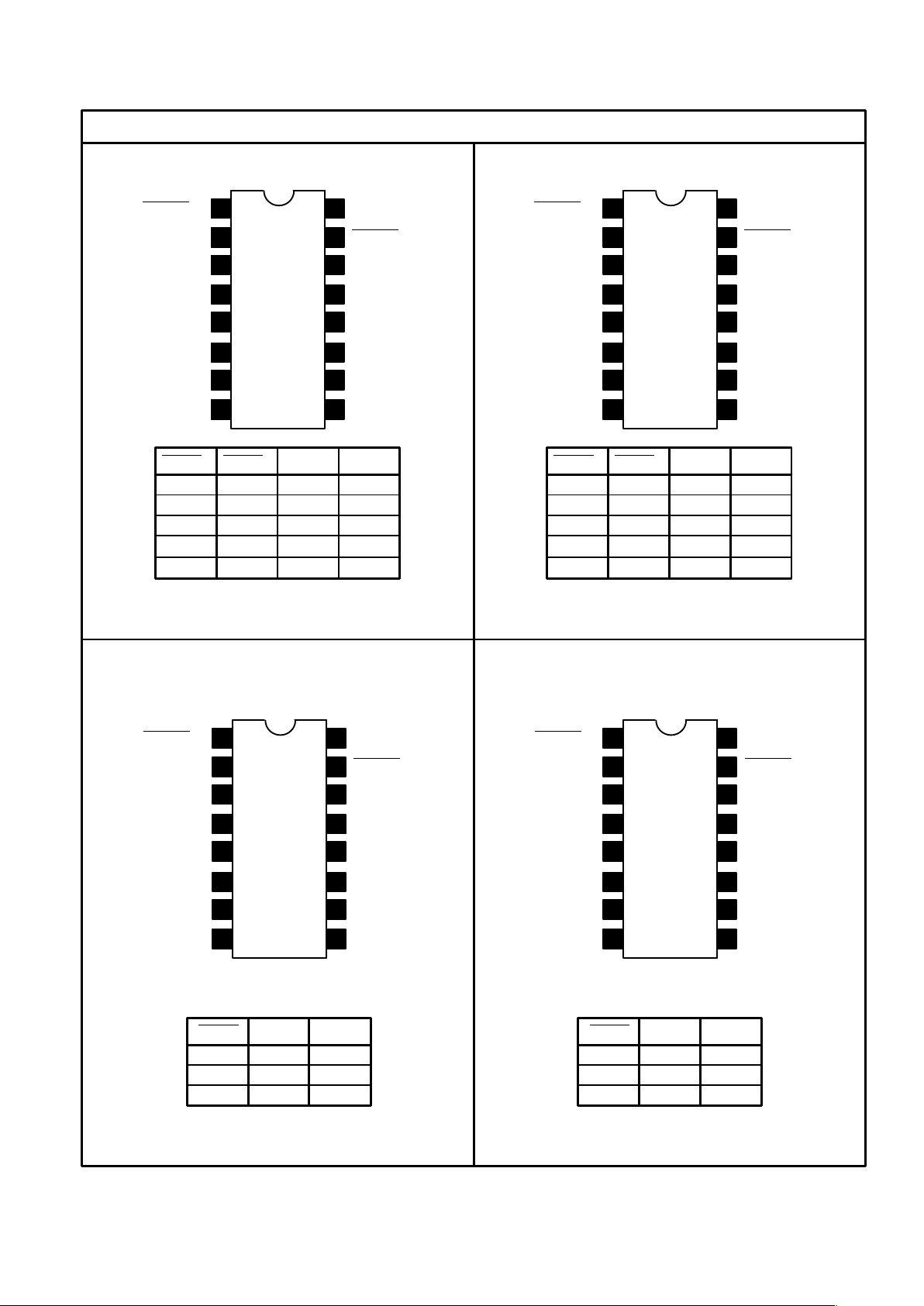
Pin Connection Diagrams and Truth Tables
NTE6885 NTE6886
NTE6887 NTE6888
Enable 2 Enable 1 Input Output
L
L
L
H
H
L
L
H
L
H
L
H
X
X
X
L
H
Z
Z
Z
L = Low Logic State
H = High Logic State
Z = Third (High Impedance) State
X = Don’t Care
Enable 2 Enable 1 Input Output
L
L
L
H
H
L
L
H
L
H
L
H
X
X
X
H
L
Z
Z
Z
L = Low Logic State
H = High Logic State
Z = Third (High Impedance) State
X = Don’t Care
Enable Input Output
L
L
H
L
H
X
L
H
Z
L = Low Logic State
H = High Logic State
Z = Third (High Impedance) State
X = Don’t Care
Enable Input Output
L
L
H
L
H
X
H
L
Z
L = Low Logic State
H = High Logic State
Z = Third (High Impedance) State
X = Don’t Care
Output D
Output E
Output C
Output B
Output A
Input A
Input F
GND
1
2
3
4Input B
5
6Input C
7
8
16
15
14
13
12 Input E
11
10 Input D
9
Output F
Enable 2
V
CC
Enable 1
Output D
Output E
Output C
Output B
Output A
Input A
Input F
GND
1
2
3
4Input B
5
6Input C
7
8
16
15
14
13
12 Input E
11
10 Input D
9
Output F
Output D
Output E
Output C
Output B
Output A
Input A
Input F
GND
1
2
3
4Input B
5
6Input C
7
8
16
15
14
13
12 Input E
11
10 Input D
9
Output F
Enable 2
V
CC
Enable 4
Output D
Output E
Output C
Output B
Output A
Input A
Input F
GND
1
2
3
4Input B
5
6Input C
7
8
16
15
14
13
12 Input E
11
10 Input D
9
Output F
Page 4
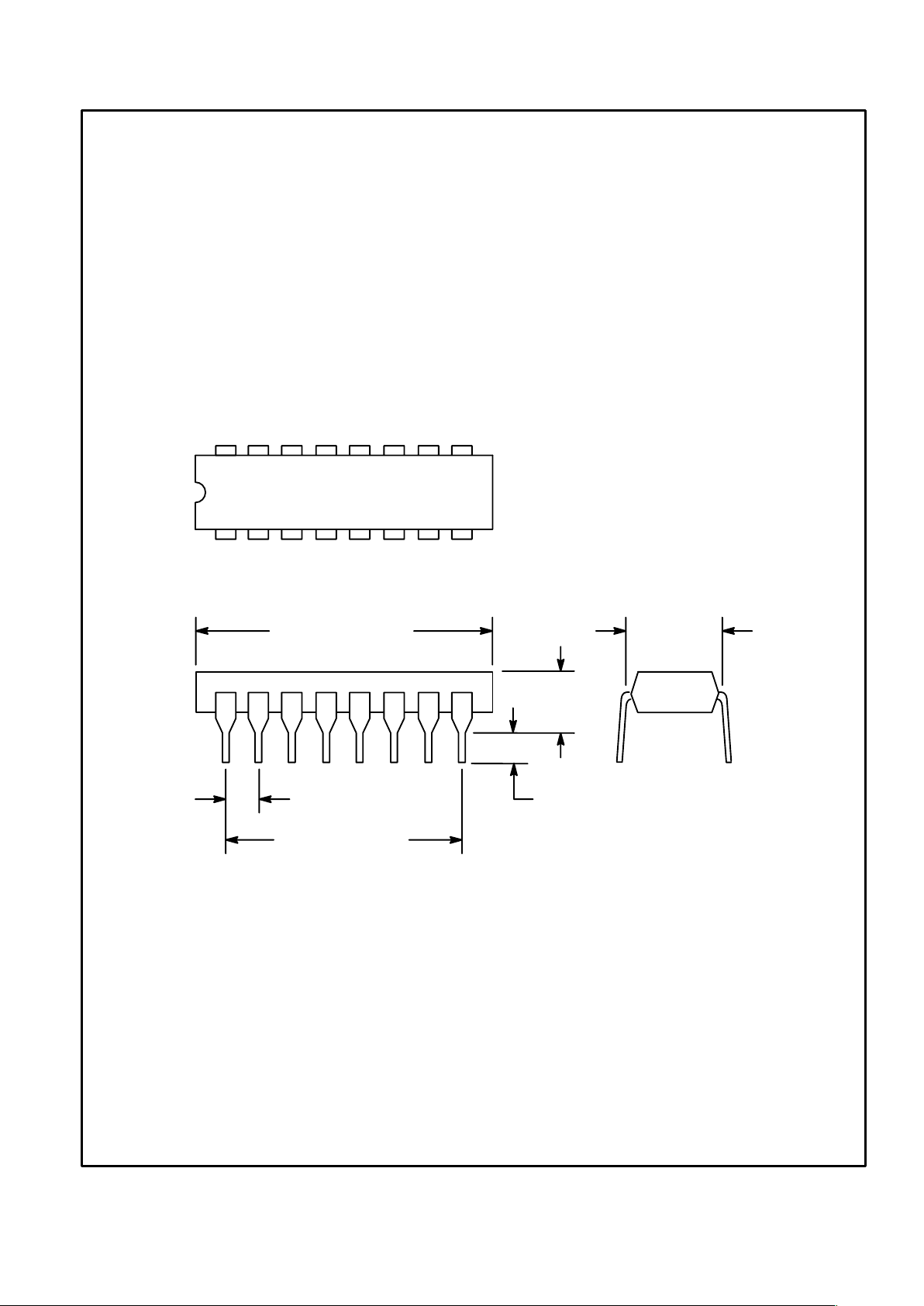
.700 (17.78)
.100 (2.54)
18
16 9
.200 (5.08)
Max
.870 (22.0) Max
.260 (6.6)
Max
.099 (2.5) Min
 Loading...