

Page 1

NTE6507
Integrated Circuit
NMOS, 8 Bit Microprocessor (MPU)
w
/On–Chip Clock OSC
Description:
The NTE6507 integrated circuit is an 8 bit microprocessor in a 28–Lead DIP type package which provides a selection of addressable memory range, interrupt input options, and on–chip clock oscillators
and drivers. This device is bus compatible with the MC6800 product offering and is aimed at high
performance, low cost applications where single phase inputs or crystals provide the time base.
Features:
D Single 5V ±5% Power Supply
D N Channel, Silicon Gate, Depletion Load
Technology
D 8 Bit Parallel Processing
D Decimal and Binary Arithmetic
D Thirteen Addressing Modes
D True Indexing Capability
D Programmable Stack Pointer
D Variable Length Stack
D Bi–Directional Data Bus
D Instruction Decoding and Control
D 8k Addressable Bytes of Memory
D “Ready” Input
D Direct Memory Access Capability
D Bus Compatible with MC6800
D On–Board Clock
D 1MHz Operating Frequency
Absolute Maximum Ratings:
Supply Voltage, V
Input Voltage, V
Operating Temperature Range, T
Storage Temperature Range, T
Note 1. This device contains input protection against damage due to high static voltages or electric
fields; however , precautions should be taken to avoid application of voltages higher than the
maximum rating.
CC
in
(Note 1)
A
stg
–0.3 to +7.0V. . . . . . . . . . . . . . . . . . . . . . . . . . . . . . . . . . . . . . . . . . . . . . . . . . . . . . .
–0.3 to +7.0V. . . . . . . . . . . . . . . . . . . . . . . . . . . . . . . . . . . . . . . . . . . . . . . . . . . . . . . . . .
0 to +70°C. . . . . . . . . . . . . . . . . . . . . . . . . . . . . . . . . . . . . . . . . . . . . .
–55° to +150°C. . . . . . . . . . . . . . . . . . . . . . . . . . . . . . . . . . . . . . . . . .
Page 2
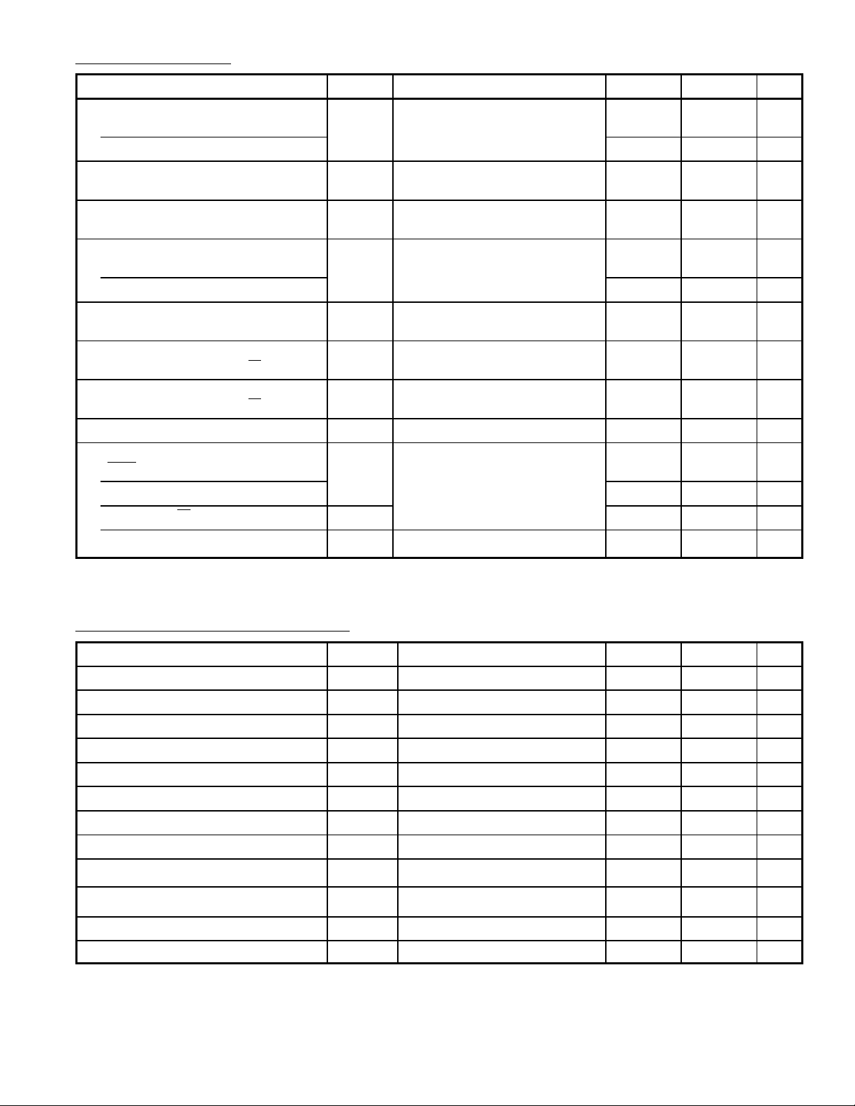
DC Characteristics: (VCC = 5V ±5%, TA = 0° to +70°C unless otherwise specified)
Parameter Symbol Test Conditions Min Max Unit
Input High Voltage
Logic and ∅
o(in)
V
IH
+2.0 V
CC
Logic VCC–0.5 VCC+0.25 V
Input Low Voltage
Logic and ∅
o(in)
Input Loading
RDY
Input Leakage Current
Logic (Excluding RDY)
∅
o(in)
Three–State (Off State) Input Current
DB0–DB7
Output High Voltage
DB0–DB7, A0–A15, R/W
Output Low Voltage
DB0–DB7, A0–A15, R/W
Power Dissipation P
Capaticance
, RDY, C
RES
V
IL
–0.3 +0.8 V
I
Vin = 0V, VCC = 5.25V
IL
–10 –300 µA
I
Vin = 0 to 5.25V, VCC = 0
in
– 2.5 µA
– 10.0 µA
I
TSI
Vin = 0.4 to 2.4V, VCC = 5.25V
– ±10 µA
V
OH
I
= –100µA, VCC = 4.75V
LOAD
2.4 – V
V
OL
I
= 1.6mA, VCC = 4.75V
LOAD
– 0.4 V
VCC = 5.25V – 700 mW
D
Vin = 0, TA = +25°C, f = 1MHz
in
– 10 pF
DB0–DB7 – 15 pF
V
A0–A15, R/W C
∅
o(in)
C
O
out
o(in)
– 12 pF
– 15 pF
Dynamic Operating Characteristics: (VCC = 5V ±5%, TA = 0° to +70°C unless otherwise specified)
Parameter Symbol Test Conditions Min Max Unit
Cycle Time T
∅
Low Time T
o(in)
∅
High Time T
o(in)
∅o Neg to ∅1 Pos Delay T
∅o Neg to ∅2 Neg Delay T
∅o Pos to ∅1 Neg Delay T
∅o Pos to ∅2 Pos Delay T
∅
Rise and Fall Time TRO, T
α
(in)
∅
∅
Delay Between ∅1 and ∅
1(OUT)
2(OUT)
Pulse Width
Pulse Width
2
T
T
CYC
L∅o
H∅o
01+
02–
01–
02+
PWHO
PWHO
T
D
∅1 and ∅2 Rise and Fall Times TR, T
Note 2 480 – ns
Note 2 460 – ns
Load = 100pF 10 70 ns
Load = 100pF 5 65 ns
Load = 100pF 5 65 ns
Load = 100pF 15 75 ns
Note 3 0 30 ns
FO
1
2
Load = 1TTL load +30pF, Note 3 – 25 ns
F
1.00 40 µs
T
–20
LO
o
T
LO
o
–40 T
T
LO
o
–10
LO
o
5 – ns
ns
ns
Note 2. Measured at 50% points.
Note 3. Measured between 10% and 90% points.
Page 3

Dynamic Operating Characteristics (Cont’d): (VCC = 5V ±5%, TA = 0 to +70°C unless otherwise
specified)
Parameter Symbol Test Conditions Min Max Unit
R/W Setup Time T
R/W Hold Time T
Address Setup Time T
Address Hold Time T
Read Access Time T
Read Data Setup Time T
Read Data Hold Time T
Write Data Setup Time T
Write Data Hold Time T
Sync Setup Time T
Sync Hold Time T
RDY Setup Time T
RWS
RWH
ADS
ADH
ACC
DSU
HR
MDS
HW
SYS
SYH
RS
Note 4 200 – ns
Note 4. RDY must never switch states within TRS to end of ∅2.
Pin Connection Diagram
– 225 ns
30 – ns
– 225 ns
30 – ns
– 650 ns
100 – ns
10 – ns
20 175 ns
60 150 ns
– 350 ns
30 – ns
Ø 2 (Out)RES
28
27
Ø 0 (In)
R/W
26
DB 0
25
DB 1
24
23 DB 2
22 DB 3
DB 4
DB 5
DB 6
V
SS
RDY
V
CC
AB 0
AB 1
AB 2
AB 3
AB 4
AB 5
1
2
3
4
5
6
7
8 21
9 20
10 19
AB 6 11 18 DB 7
AB 7 AB 12
AB 8 AB 11
12 17
13 16
AB 9
14 15
AB 10
Page 4

14 1
15 28
1.469 (37.32)
.100 (2.54)
1.300 (33.02)
Max
.250
(6.35)
.122
(3.1)
Min
.540
(13.7)
.600
(15.24)
 Loading...