

Page 1
NTE1577
Integrated Circuit
Dual, Low Noise Preamp
w
/Auto Reverse
Description:
The NTE1577 is a dual preamplifier with tape autoreverse facilityin a 16–Lead D IP type package designed f or the a mpli fication o f l ow l evel s ignal s i n a ppli cations r equiring v ery l ow n ois e p erfor mance, a s
stereo c assette p layers. E ach c hannel c onsists o f t wo i ndependent a mplifier s. The f irst h as a f ixed g ain
of 30dB while the second one is an operational amplifier optimized for high quality audio application.
Features:
D Very Low Noise
D High Gain
D Large Output Voltage Swing
D Low Distortion
D Tape Autoreverse Facility
D Single Supply Operation
D Short Circuit Protection
D Wide Supply Range
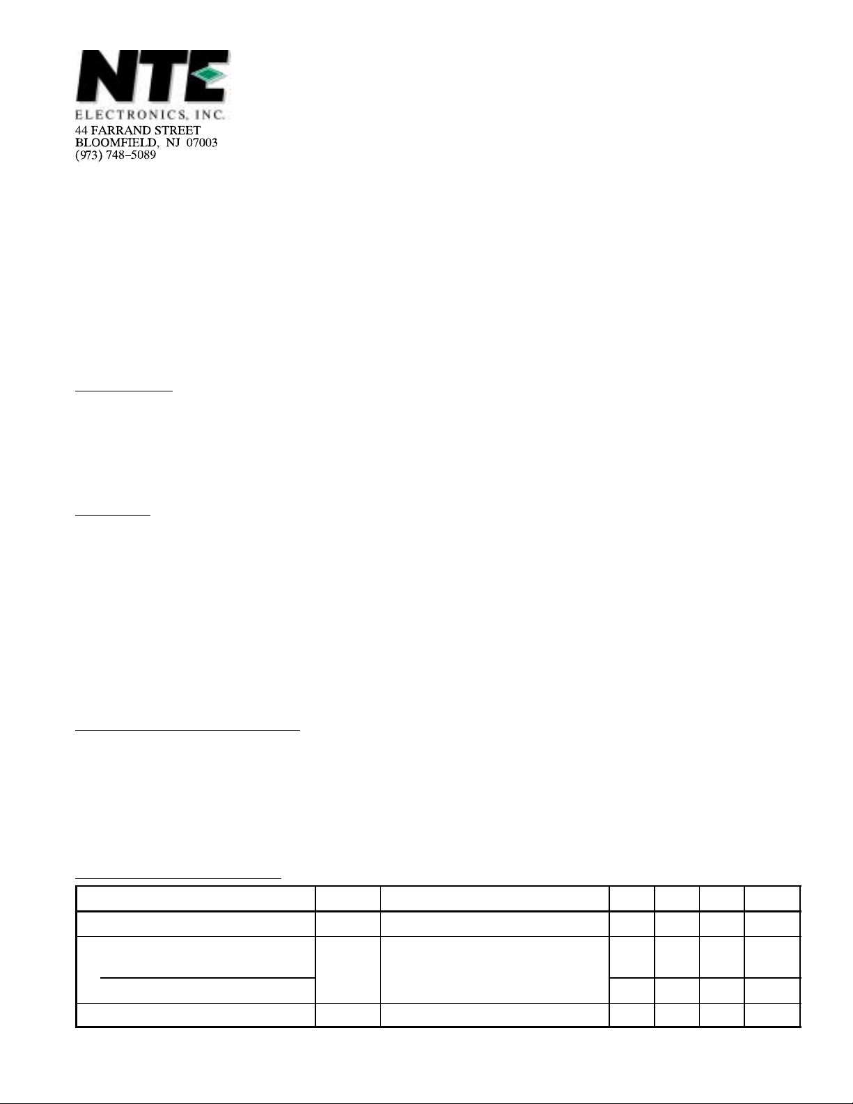
Absolute Maximum Ratings:
Supply Voltage, V
Total Power Dissipation (TA = +60°C), P
Operating Junction Temperature Range, T
Storage Temperature Range, T
Thermal Resistance, Junction–to–Ambient, R
S
600mW. . . . . . . . . . . . . . . . . . . . . . . . . . . . . . . . . . . . . . . . . . .
150°C/W. . . . . . . . . . . . . . . . . . . . . . . . . . . . . . . . . .
stg
D
J
–40° to +150°C. . . . . . . . . . . . . . . . . . . . . . . . . . . . . . . . . .
–40° to +150°C. . . . . . . . . . . . . . . . . . . . . . . . . . . . . . . . . . . . . . . . . .
thJA
Electrical Characteristics: (TA = +25°C, VS = 14.4V, GV = 60dB unless otherwise specified)
Parameter Symbol Test Conditions Min Typ Max Unit
Supply Current I
Output Current (Pin1 to Pin15)
Source
Sink – 1 – mA
Closed Loop Gain G
I
VS = 8V to 30V – 10 – mA
S
O
VS = 8V to 30V – 10 – mA
f = 20Hz to 20kHz – 60 – dB
V
36V. . . . . . . . . . . . . . . . . . . . . . . . . . . . . . . . . . . . . . . . . . . . . . . . . . . . . . . . . . . . . . . . .
Page 2
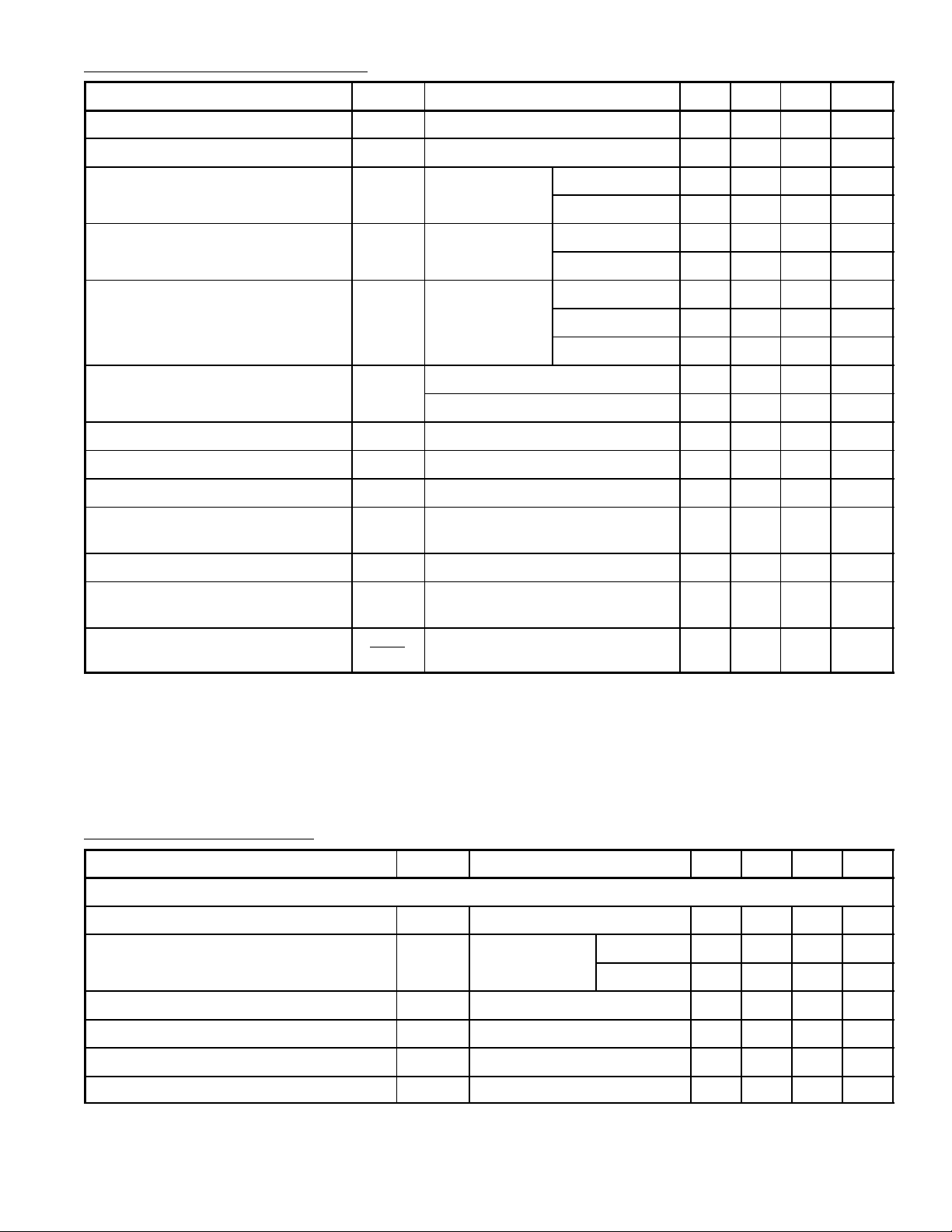
Electrical Characteristics (Cont’d): (TA = +25°C, VS = 14.4V, GV = 60dB unless otherwise specified)
Parameter Symbol Test Conditions Min Typ Max Unit
Input Resistance R
Output Resistance (pins 1–15) R
Total Harmonic Distortion
THD VO = 300mV
f = 1kHz 50 80 – kΩ
i
f = 1kHz – 50 – Ω
o
f = 1kHz – 0.05 – %
f = 10kHz – 0.05 – %
Output Voltage Swing V
(Pin1 to Pin15)
Total Input Noise
Peak–to–Peak
O
e
Note 1 Rg = 50Ω – 0.25 – µV
n
VS = 14.4V – 12 – V
VS = 30V – 28 – V
Rg = 600Ω – 0.4 0.6 µV
Rq = 5kΩ – 1.3 – µV
Signal–to–Noise Ratio
S/N
Vin = 0.3mV, Rg = 600Ω, Note 1 – 57 – dB
Vin = 1mV, Rg = 0, Note 1 – 73 – dB
Channel Separation CS f = 1kHz – 60 – dB
Crosstalk (Differential Input) CT f = 1kHz, Note 3 – 80 – dB
Supply Voltage Rejection SVR f = 1kHz, Rg = 600Ω, Note 2 – 120 – dB
Supply Voltage Rejection of
SVR f = 1kHz, Rg = 600Ω, Note 2 – 100 – dB
Reference Voltage (Pin4)
Reference Voltage (Pin 4) V
Reference Voltage Output
R
ref
ref
– 55 – mV
– 100 – Ω
Resistance (Pin4)
Voltage Temperature Coefficient ∆V
ref
– 10 – µV/°C
∆T
Note 1. The weighting filter used for the noise measurement has a curve A frequency response.
Note 2. Referred to the input
Note 3. Between a disabled input and an input ON.
Electrical Characteristics: (VS = 30V unless otherwise specified)
Parameter Symbol Test Conditions Min Typ Max Unit
Amplifier No. 1
Gain (Pin6 to Pin5) G
V
Distortion d VO = 300mV
Total Input Noise e
Output Impedance (Pin5) Z
Output Current (Pin5) I
DC Output Voltage (Pin5) V
Rg = 600Ω, Note 1 – 0.4 – µV
n
f = 1kHz – 100 – Ω
O
O
VS = 10V 1.3 2 2.7 V
5
f = 1kHz – 0.05 – %
f = 10kHz – 0.05 – %
29 30 30.5 dB
– 1 – mA
Note 1. The weighting filter used for the noise measurement has a curve A frequency response.
Page 3

Electrical Characteristics (Cont’d): (VS = 30V unless otherwise specified)
Parameter Symbol Test Conditions Min Typ Max Unit
Amplifier No. 2
Open Loop Voltage Gain (Pin2 to Pin1) G
Input Bias Current I
Input Offset Voltage V
Input Offset Current I
Small Signal Bandwidth BW GV = 30dB – 150 – kHz
Total Input Noise e
Input Impedance R
B
OS
os
V
Rg = 600Ω, Note 1 – 2 – µV
n
f = 1kHz (Open Loop) 150 500 – kΩ
I
– 100 – dB
– 0.2 – µA
– 2 – mV
– 0.05 – µA
Note 1. The weighting filter used for the noise measurement has a curve A frequency response.
Autoreverse:
P
in
6 – 10 OFF ON
7 – 9 ON OFF
Pin Connection Diagram
V12 < 2V V12 > 4.5V
Output A
Non–Inverting Input A
Inverting Input A
Voltage Reference
1
2
3
4
5Output
6Input
7Input
V
16
CC
15
Output B
14
Non–Inverting Input B
13
Inverting Input B
12 Threshold
11 Output
10 Input
8GND 9 Input
Page 4

16 9
.260 (6.6) Max
18
.245
(6.22)
Min
.785 (19.9)
Max
.100 (2.54)
.700 (17.7)
.300
(7.62)
.200 (5.08)
Max
 Loading...