

Page 1

DATA SHEET
TFT COLOR LCD MODULE
NL6448BC33-31
26 cm (10.4 inches), 640
××××
480 pixels, 262,144 colors,
Incorporated two-lamp/Edge-light type backlight
Wide viewing angle
DESCRIPTION
NL6448BC33-31 is a TFT (thin film transistor) active matrix color liquid crystal display (LCD) comprising
amorphous silicon TFT attached to each signal electrode, a driving circuit and a backlight. NL6448BC33-31 has a
built-in backlight. Backlight includes long-life-lamps and the lamps are replaceable.
The 26 cm (10.4 inches) diagonal display area contains 640 × 480 pixels and can display 262,144 colors
simultaneously.
NL6448BC33-31 is suitable for industrial application use because of the wide viewing angle and the high
luminance. Also, the viewing direction is selectable either upper or lower side by changing scan direction.
NL6448BC33-31 interface is compatible with NL6448AC33-18, -18A, -18B and -27.
FEATURES
• Wide viewing angle (with Retardation Film)
• Smooth polarizer surface (No antiglare treatment)
• High luminance (350 cd/m2, typ.: saturated value, at
room temp.)
• Low reflection
• 6-bit digital RGB signals
• Data enable function
• Backlight with two long-life-time lamps (one lamp
holder, inverter-less)
• Lamp holder replaceable (Type No.: 104LHS31)
• Reversible scan direction (with DPS pin)
• Replaceable lamp holders (Type No.: 104LHS31)
• Recommended inverter (Part No.: 104PWRI)
• Best viewing angle select function (with MVA terminal)
• Luminance control
• Easy to attach a touch panel
APPLICATIONS
• Display terminals for control system
• Monitors for process controller
• Industrial PCs
The information in this document is subject to change without notice.
Document No. EN0443EJ1V0DS00 (1st edition)
Date Published July 1999 P
Printed in Japan
1999©
Page 2

NL6448BC33-31
STRUCTURE AND FUNCTIONS
A color TFT (thin film transistor) LCD module is comprised of a TFT liquid crystal panel structure, LSIs for driving
the TFT array, and a backlight assembly. The TFT panel structure is created by sandwiching liquid crystal material
in the narrow gap between a TFT array glass substrate and a color filter glass substrate. After the driver LSIs are
connected to the panel, the backlight assembly is attached to the backside of the panel.
RGB (red, green, blue) data signals from a source system is modulated into a form suitable for active matrix
addressing by the onboard signal processor and sent to the driver LSIs which in turn addresses the individual TFT
cells.
Acting as an electro-optical switch, each TFT cell regulates light transmission from the backlight assembly when
activated by the data source. By regulating the amount of light passing through the array of red, green, and blue
dots, color images are created with clarity.
OUTLINE OF CHARACTERISTICS (at room temperature)
Display area 211.2 (H) × 158.4 (V) mm
Drive system a-Si TFT active matrix
Display colors 262,144 colors
Number of pixels 640 × 480 pixels
Pixel arrangement RGB vertical stripe
Pixel pitch 0.33 (H) × 0.33 (V) mm
Module size 243.0 (H) × 185.1 (V) × 10.75 typ. (D) mm
Weight 530 g (typ.)
Contrast ratio 300 : 1 (typ.)
Viewing angle (more than the contrast ratio of 10 : 1)
Horizontal : 50° (typ., left side, right side)
Vertical : 40° (typ., up side), 45° (typ, down side)
Designed viewing direction Wider viewing angle without image reversal: up side (12 o’clock normal scan)
down side (6 o’clock reverse scan)
Wider viewing angle with contrast ratio : down side (6 o’clock normal scan)
up side (12 o’clo ck re vers e scan )
Optimum grayscale (
Polarizer pencil-hardness 2H (Min., at JIS K5400)
Color gamut 43% (typ. at center, to NTSC)
Response time 15 ms (typ.), white to black
Luminance 350 cd/m
Signal system 6-bit digital signals for each of RGB primary colors, synchronous signals
(Hsync, Vsync), dot clock (CLK)
Supply voltages 3.3 V [5.0 V] (Logic, LCD driving), 12.0 V (Backlight)
Backlight Edge light type, two cold cathode fluorescent lamps (cold cathode type)
[Replaceable parts]
Lamp holder: type No.104LHS31
Power consumption 6.8 W (typ., at 3.3 V, 12.0 V)
2
(TYP)
= 2.2) : perpendicular
γ
2
Data Sheet EN0443EJ1V0DS00
Page 3
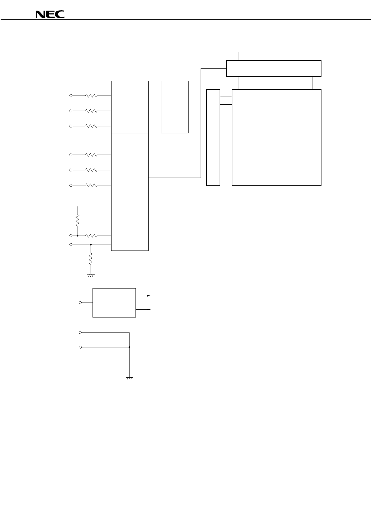
BLOCK DIAGRAM
100 Ω
R0-R5
100 Ω
G0-G5
100 Ω
B0-B5
100 Ω
CLK
100 Ω
H sync
100 Ω
V sync
Digital
signal
processor
LCD timing
controller
Level
shift
·
·
·
·
V-driver
·
· · · · · ·
TFT LCD panel
H: 640 × 3 (R. G. B)
V: 480
480 lines
NL6448BC33-31
H-driver
1920 lines
DE
DPS
V
CC
GND (SG)
Frame (FG)
VCC
47 kΩ
100 Ω
47 kΩ
Power
supply
circuit
LSIs (V
Drivers
CCi
: 3.3 V)
Data Sheet EN0443EJ1V0DS00
3
Page 4
VH
VL
VH
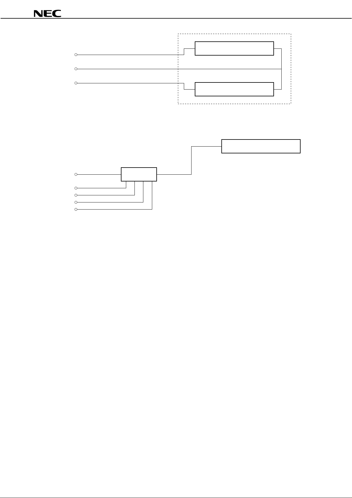
<In case of connecting NEC recommended inverter>
InverterVDDB
BRTC
BRTL
BRTH
GNDB
NL6448BC33-31
Lamp
Lamp
Backlight
Backlight
(Part No. 104PWBR1)
4
Data Sheet EN0443EJ1V0DS00
Page 5
NL6448BC33-31
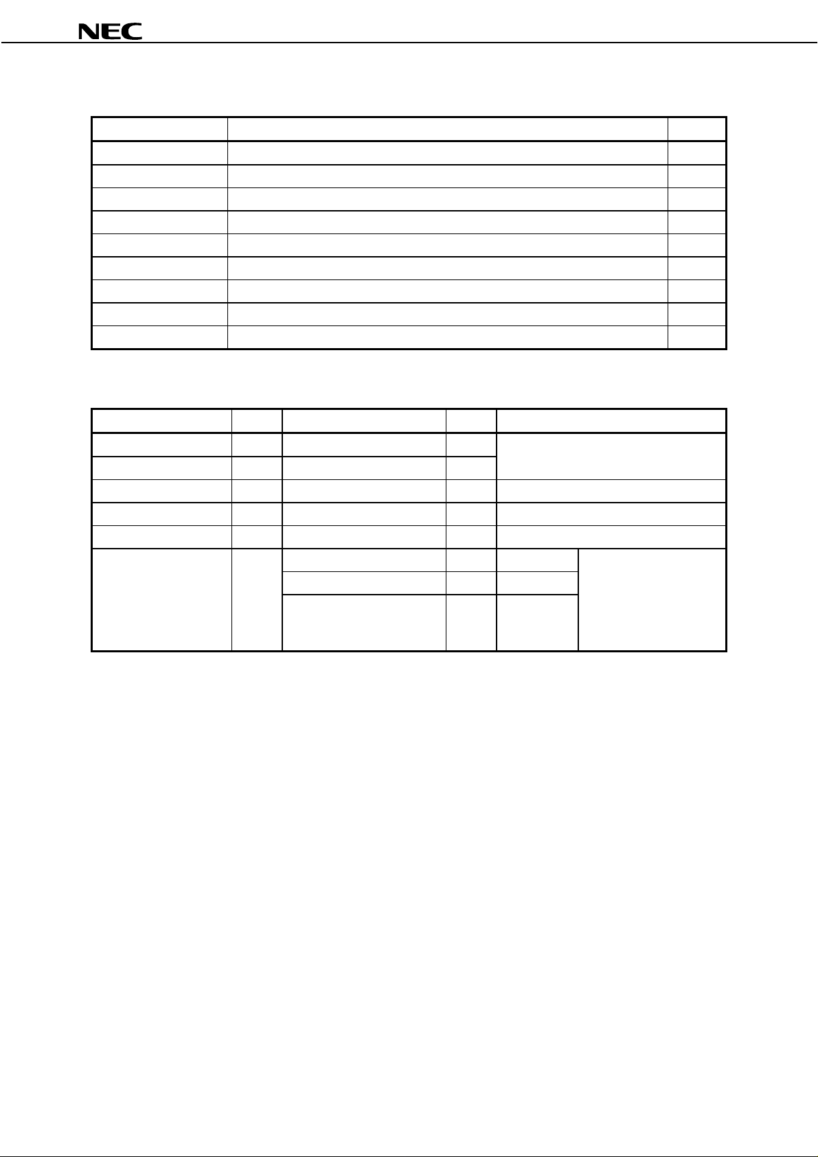
GENERAL SPECIFICATIONS
Items Specifications Unit
Module size 243.0 ± 0.5 (H) × 185.1 ± 0.5 (V) × 11.5 max. (D) mm
Display area 211.2 (H) × 158.4 (V) mm
Number of dots 640 × 3 (H) × 480 (V) dot
Number of pixels 640 (H) × 480 (V) pixel
Dot pitch 0.11 (H) × 0.33 (V) mm
Pixel pitch 0.33 (H) × 0.33 (V) mm
Pixel arrangement RGB (Red, Green, Blue) vertical stripe –
Display colors 262,144 color
Weight 550 (max.) g
ABSOLUTE MAXIMUM RATINGS
Parameters Symbols Ratings Unit Remarks
Supply voltage V
Input voltage V
Lamp voltage V
Storage temp. T
Operating temp. T
Humidity
(no condensation)
Measured at the display area
Note
RH
CC
I
L
ST
OP
–0.3 to VCC +0.3 V
≤
95% relative humidity – T
≤
85% relative humidity –
Absolute humidity shall not
exceed T
a
relative humidity level.
–0.3 to 6.5 V
2000 V
–20 to 60
0 to 50
= 50°C, 85%
a
T
= 25°C
rms
°
C
Module surface
°
C
a
≤ 40°C
40 < Ta ≤ 50°C
a
–T
> 50°C
−
Note
No condensation
Data Sheet EN0443EJ1V0DS00
5
Page 6
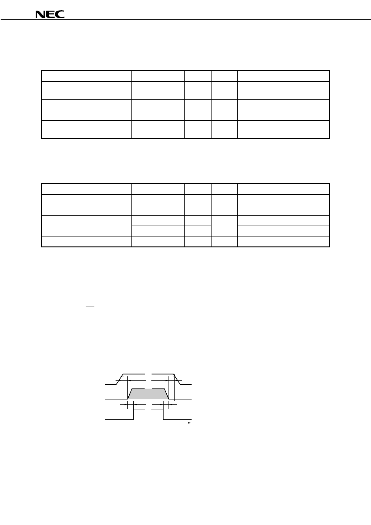
ELECTRICAL CHARACTERISTICS
(1) Logic, LCD driving
Parameters Symbols MIN. TYP. MAX. Unit Remarks
NL6448BC33-31
Ta = 25°C
Supply voltage V
Logic input Low voltage V
Logic input High voltage V
Supply current I
Checkered flag pattern (in EIAJ ED-2522)
Note
(2) Backlight
Parameters Symbols MIN. TYP. MAX. Unit Remarks
Lamp current I
Lamp voltage V
Oscillator frequency F
Recommended value of “F
Note
•Ft is within the specification.
CC
IL
IH
CC
L
L
S
t
3.0
(4.75)
0–V
VCC × 0.7 – 5.25 V
–
–
2.0 5.0 5.5 mArms with one lamp
−
840
1265
50 54 58 kHz
t
”.
3.3
(5.0)
325
Note
(250)
510
−−
−−
3.6
(5.25)
CC
× 0.3 mV
370
(300)
−
VVCC = 3.3 V
CC
= 5.0 V)
(V
CMOS level
mA VCC = 3.3 V
CC
= 5.0 V)
(V
Vrms
Vrms
a
T
= 25°CLamp turn on voltage V
Ta = 0°C
Note
a
= 25°C
T
−
and
1
Ft =
•
4th
× (2n – 1)
If Ft is out of the recommended value, interference between Ft frequency and Hsync frequency may cause
beat on the display.
SUPPLY VOLTAGE SEQUENCE
Signals
Backlight
V
Notes 1, 2, 3
Note 4
3.0 V (4.75 V)
CC
0 V
0 V
0 < t < 35 ms 0 < t < 35 ms
ON OFF
thn: Hsync period
: a natural number (1, 2, 3, ····)
3.0 V (4.75 V)
VALID
2tV < t
0 < t
Time
otes 1.
Signals: CLK, Hsync, Vsync, DE,
DATA (R0-R5, G0-G5, B0-B5)
The supply voltage for input signals
2.
CC
should be the same as V
Apply VDDB within the LCD operation
3.
.
period. When the backlight turns on
before LCD operation or the LCD
operation turns off before the backlight
turns off, the display may momentarily
become white.
While the power is off, please keep
4.
whole signals at low level or high
impedance.
6
Data Sheet EN0443EJ1V0DS00
Page 7
NL6448BC33-31
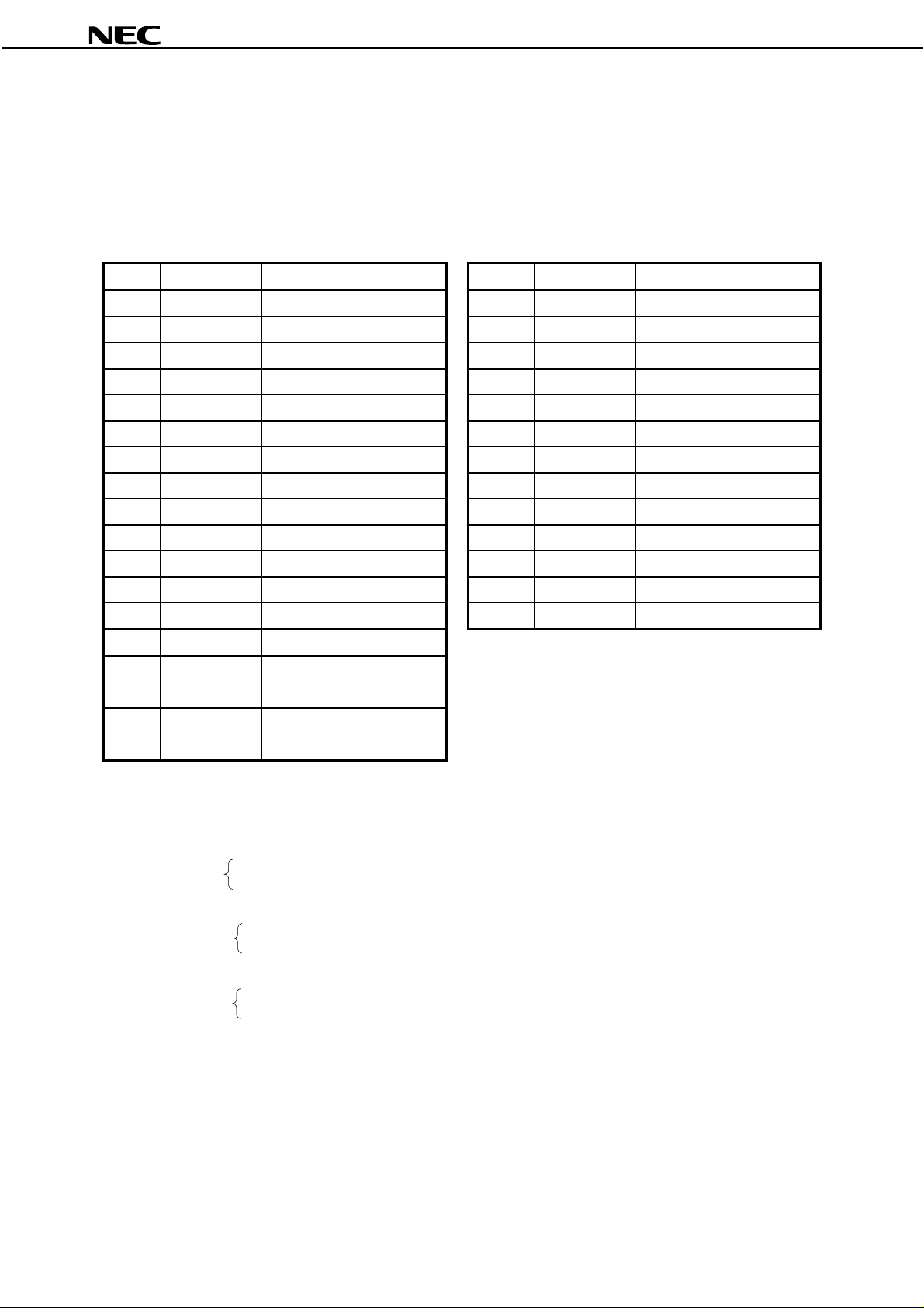
INTERFACE PIN CONNECTIONS
(1) Interface signals, power supply
Module side connector Mating connector
CN1 ··· DF9C-31P-1V (No.1 to 30) DF9-31S-1V or DF9M-31S-1R ...... (1)
IL-310-T31S-VF ...... (2)
Supplier: (1) HIROSE ELECTRIC CO., LTD., (2) Japan Aviation Electronics Industry Limited (JAE)
Pin No. Symbols Functions Pin No. Symbols Functions
1 GND Ground 19 GND Ground
2 CLK Dot clock 20 B0 Blue data (LSB)
3 Hsync Horizontal sync. 21 B1 Blue data
4 Vsync Vertical sync. 22 B2 Blue data
5 GND Ground 23 B3 Blue data
6 R0 Red data (LSB) 24 B4 Blue data
7 R1 Red data 25 B5 Blue data (MSB)
8 R2 Red data 26 GND Ground
9 R3 Red data 27 DE Data enable
10 R4 Red data 28 V
11 R5 Red data (MSB) 29 V
12 GND Ground 30 MVA Best Viewing Select
13 G0 Green data (LSB) 31 DPS Scan direction select
CC
CC
Power supply
Power supply
14 G1 Green data
15 G2 Green data
16 G3 Green data
17 G4 Green data
18 G5 Green data (MSB)
CC
: All VCC terminals should be connected to 3.3V or 5.0 V.
Notes 1.
V
GND is connected to the frame of the LCD module.
2.
DE: DE/Fixed mode select is as follows.
3.
Data enable signal = DE mode
CC
or Open = Fixed mode
V
MVA: MVA changes best viewing angle at gray scale screen.
4.
CC
or Open = Perpendiculer (best viewing angle: 0°)
V
GND = down side (best viewing angle: −10°)
DPS: DPS changes display scan direction.
5.
GND or Open = Scan direction will be decided by the setting of SW1.
CC
= Reverse scan
V
DISPLAY POSITION about another way for reversible scan.
CC
When DPS is V
, reverse scan is selected even if SW1 is set at normal scan.
LSB : Least Significant Bit
MSB : Most Significant Bit
Data Sheet EN0443EJ1V0DS00
7
Page 8
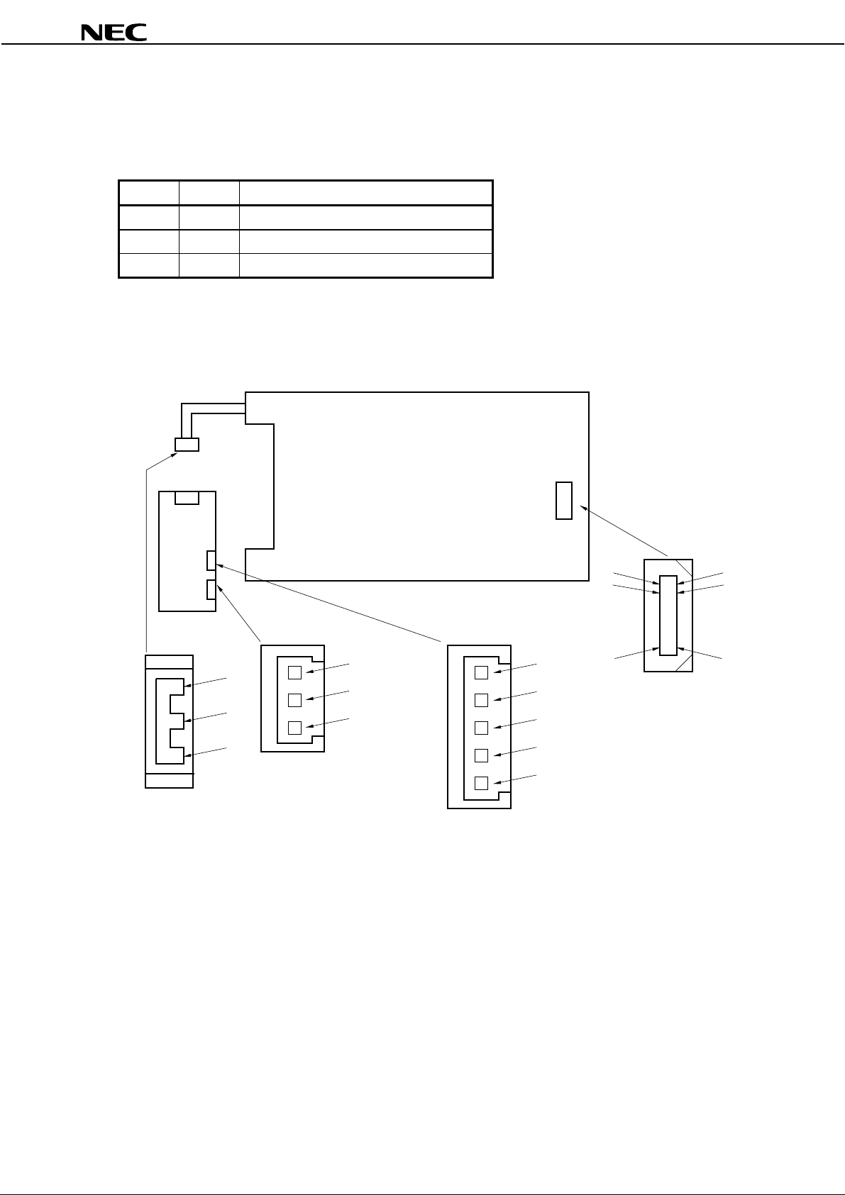
(2) Backlight
• Lamp side connector Mating connector
CN2 ··· BHR-03VS-1 SM03 (4.0)B-BHS-TB
Supplier: J.S.T TRADING COMPANY, LTD.
Pin No. Symbols Func tions
NL6448BC33-31
1V
2V
3V
L
H
H
(3) Connector locations
<Connector locations>
CN2
NEC
Recommended
inverter
CN1
CN3
Power supply (low)
Power supply (high)
Power supply (high)
1
2
1
2
3
Upper side
LCD Module
<Rear view>
Lower side
CN1
1
3
•
•
•
•
•
1
2
3
31
<Pin arrangement of CN1>
2
4
•
•
•
•
•
30
3
<Pin arrangement of CN3>
<Pin arrangement of CN2>
Incase of connecting NEC recommended inverter
8
4
5
<Pin arrangement of CN1>
Data Sheet EN0443EJ1V0DS00
Page 9
NL6448BC33-31
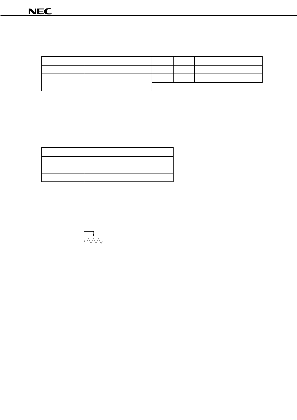
• Inverter side connector 1 Mating connector 1
CN1 ··· LZ-5P-SL-SMT LZ-5S-SC3
Supplier: Japan Aviation Electronics Industry Limited (JAE)
Pin No. Symbols Functi ons Pin No. Symbols Functions
1V
2V
3 GNDB Backlight ground
Note
DD
B Power supply (12 V) 4 GNDB Backlight ground
DD
B Power supply (12 V) 5 BRTHL
High luminance (100%): BRTHL = High (+5 V) or open
Low luminance (60%): BRTHL = Low (GNDB level)
• Inverter side connector 2 Mating connector 2
CN3 ··· IL-Z-3PL-SMTY IL-Z-3S-S125C3
Supplier: Japan Aviation Electronics Industry Limited (JAE)
Pin No. Symbols Func tions
1BRTC
2BRTH
3BRTL
Notes 1.
CMOS level
Backlight ON/OFF signal
Luminance control input
Luminance control input
Note 1
Note 2
Note 2
Backlight ON: BRTC = High (+5 V) or open
Backlight OFF : BRTC = Low (GNDB level)
<1> A way of luminance control by a variable resistor
2.
This way works when BRTHL (No.5 pin) of CN1 is opened.
Luminance select
Note
BRTL BRTH
R
Mating variable resistor
Minimum luminance (50%)
Maximum luminance (100%)
: 10 kΩ ±5%
: R = 0 Ω
: R = 10 kΩ
<2> A way of luminance control by a voltage
This way works when BRTHL and BRTL are opened. The range of input voltage between
BRTH and GNDB is as follows.
Minimum luminance (50%) : 2.5 V
Maximum luminance (100%): ≤ 1.2 V
Data Sheet EN0443EJ1V0DS00
9
Page 10
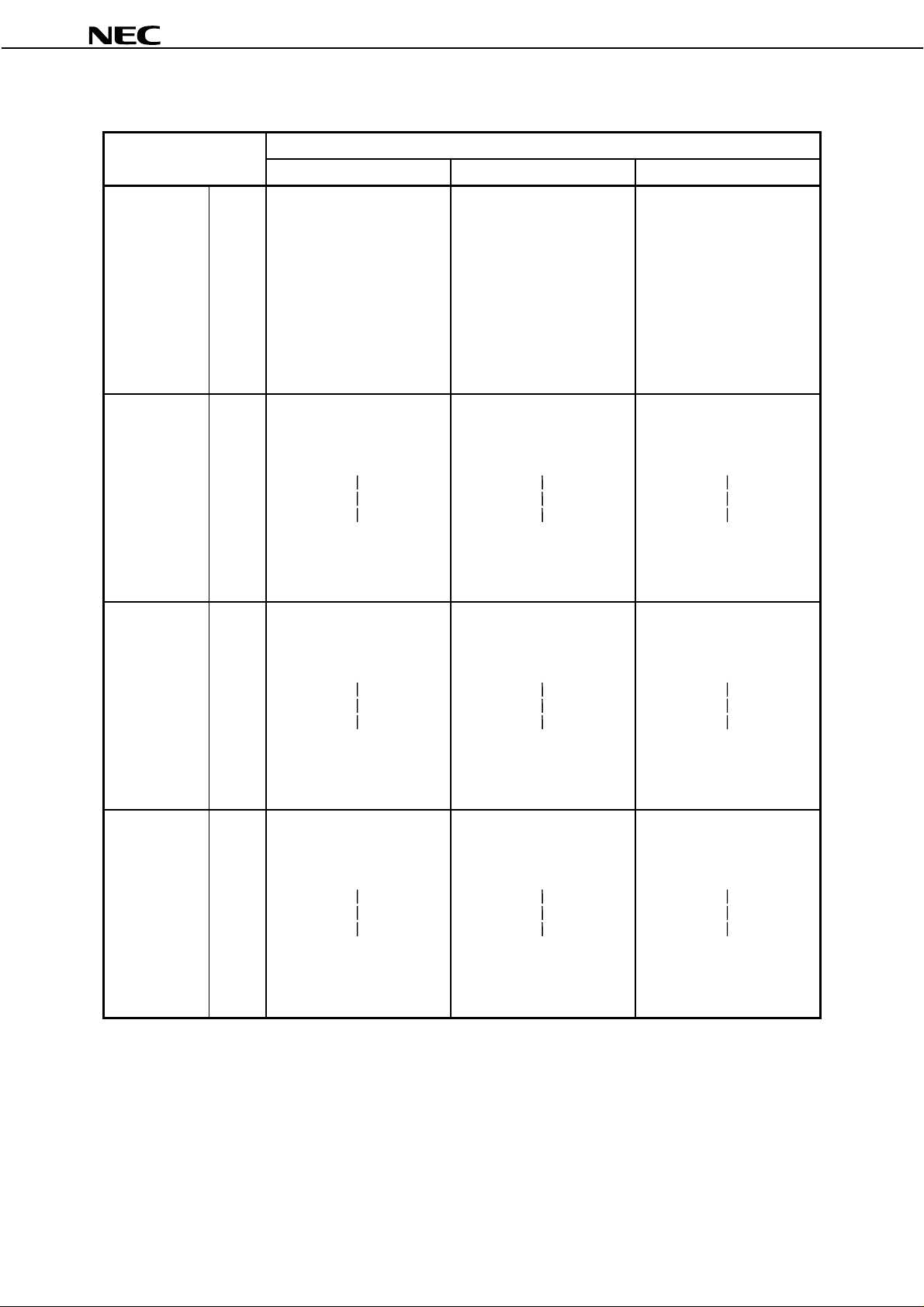
DISPLAY COLORS vs. INPUT DATA SIGNALS
NL6448BC33-31
Display colors
Basic colors
Red grayscale
Green grayscale
Blue grayscale
Data signal (0: Low level, 1: High level)
R5 R4 R3 R2 R1 R0 G5 G4 G3 G2 G1 G0 B5 B4 B3 B2 B1 B0
Black000000000000000000
Blue 000000000000111111
Red 111111000000000000
Magenta
Green000000111111000000
Cyan000000111111111111
Yellow111111111111000000
White111111111111111111
Black000000000000000000
dark 000010000000000000
bright111101000000000000
Red 111111000000000000
Black000000000000000000
dark 000000000010000000
bright000000111101000000
Green000000111111000000
Black000000000000000000
dark 000000000000000010
bright000000000000111101
Blue 000000000000111111
111111000000111111
000001000000000000
↑
↓
111110000000000000
000000000001000000
↑
↓
000000111110000000
000000000000000001
↑
↓
000000000000111110
10
The combination of 6-bit signals (64 grayscale level) results in 262144 (64 × 64 × 64) colors.
Note
Data Sheet EN0443EJ1V0DS00
Page 11
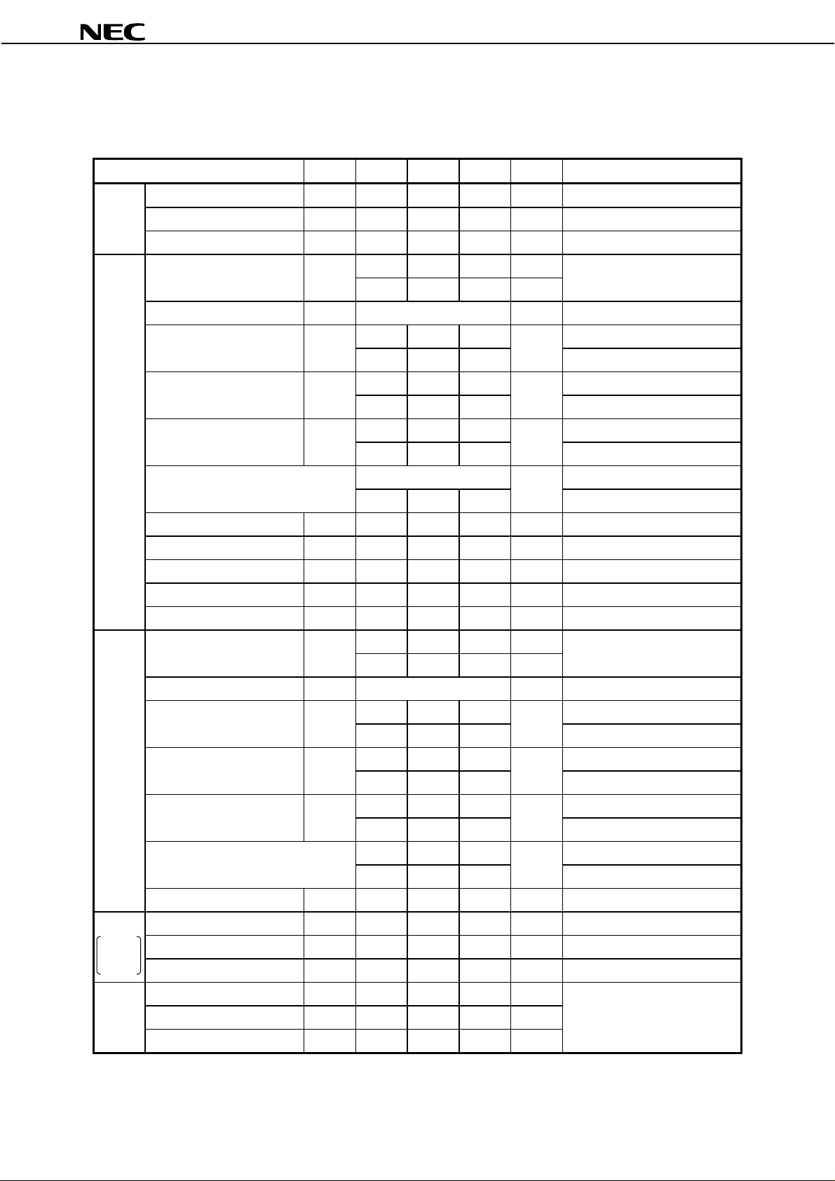
INPUT SIGNAL TIMINGS
(1) Input signal specifications (DE mode is default.)
Parameters Symbols MIN. TYP. MAX. Unit Remarks
NL6448BC33-31
CLK
Hsync
Vsync
DATA
R0-R5
G0-G5
B0-B5
DE
Frequency 1/t
Duty tch/t
Rise, fall tcrf – – 10 ns –
Display period thd 640 CLK –
CLK-Hsync ti min g thch 12 – – ns –
Hsync-CLK ti min g thcs 8 – – ns
Hsync-Vsync timing tvh 1 – – CLK
Vsync-Hsync timing tvs 30 – – ns
Rise, fall thrf – – 10 ns
Display period tvd 480 H –
Rise, fall tvrf – – 10 ns
CLK-DATA timing tds 8 – – ns
DATA-CLK timing tdh 12 – – ns
Rise, fall tdrf – – 10 ns
DE-CLK timing tes 8 – – ns
CLK-DE timing teh 12 – – ns
Rise, fall terf – – 10 ns
C
– 25.175 – MHz 39.72 ns (ty p . )
C
0.4 0.5 0.6 – –
30.0 31.778 33.6
– 800 – CLK
– 16 – Fixed modeFront-porch thf
216–
10 96 – Fixed modePul se width thp
10 96 –
– 48 134 Fixed modeBack-porch thb
448–
144 Fixed modethp + thb
14 144 –
16.1 16.683 17.2 msPeriod tv
– 525 – H
–
012–
1 2 – Fixed modePulse width tvp
12–
– 31 – Fixed modeBack-porch tvb
431–
–
533–
12
33
–
–
µ
sPeriod th
CLK
CLK
CLK
CLK
H
H
H
H
31.468 kHz (typ.)
DE mode
DE mode
DE mode
adjustable range by DE signal
59.94 Hz (typ.)
Fixed modeFront-porch tvf
DE mode
DE mode
DE mode
Fixed modetvp + tvb
DE mode
DE mode
–
–
–
–
–
–
–
–
All parameters should be kept within the specified range.
Note
Data Sheet EN0443EJ1V0DS00
11
Page 12
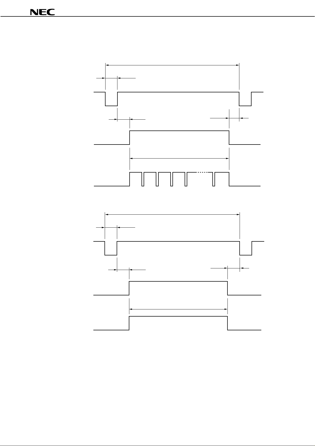
(2) Definition of input signal timings
<Vertical>
Vsync
NL6448BC33-31
tv
tvp
Display period
DE (DE mode)
<Horizontal>
Note
Hsync
thp
thb
tvb
tvf
tvd
th
thf
Notes 1.
12
Display period
DE (DE mode)
Note
thd
These do not exist as signals.
Keep thp + thb and tvp + tvb within the value shown in the table of input signal timing, otherwise
2.
display position is shifted to right or left side, or to up or down side.
Data Sheet EN0443EJ1V0DS00
Page 13
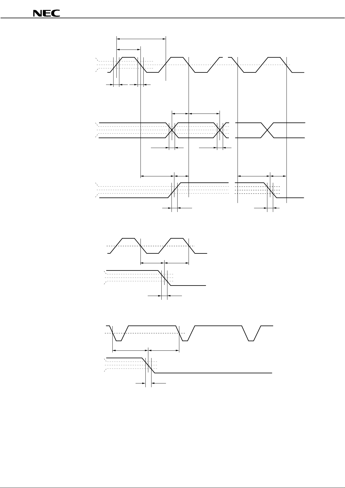
CLK
0.7 V
0.5 V
0.3 V
NL6448BC33-31
t
C
tch
CC
CC
CC
tcrf
DATA
(R0 - R5) 0.7 V
(G0 - G5) 0.5 V
(B0 - B5) 0.3 V
DE (DE mode)
CLK
Hsync
0.7 V
0.5 V
0.3 V
CC
CC
CC
CC
CC
CC
0.5 V
0.7 V
0.5 V
0.3 V
tdhtds
INVALID
INVALID
tdrftdrf
testehtesteh
terf
CC
terf
thcsthch
CC
CC
CC
thrf
Hsync
Vsync
0.5 V
0.7 V
0.5 V
0.3 V
CC
tvstvh
CC
CC
CC
tvrf
Data Sheet EN0443EJ1V0DS00
13
Page 14
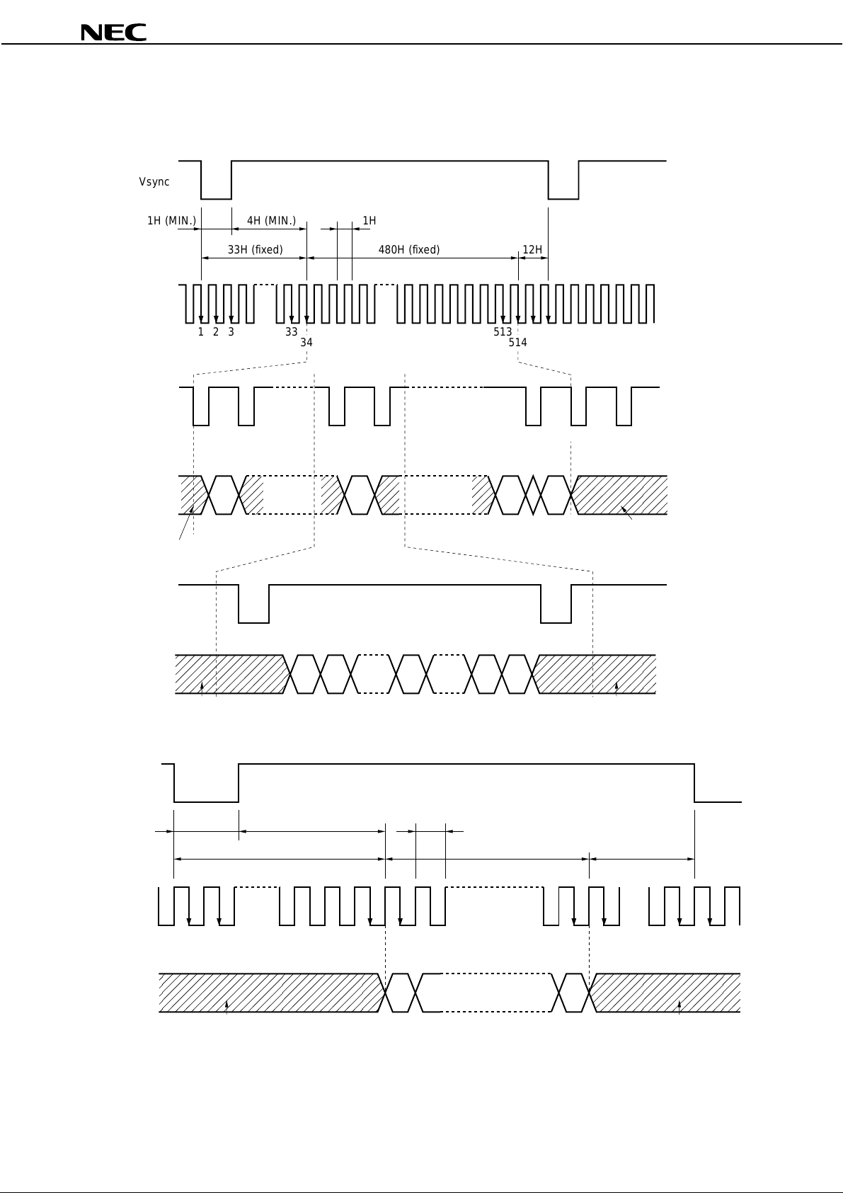
(3) Input signal timing chart
(a) Fixed mode
Vsync
1H (MIN.) 4H (MIN.) 1H
33H (fixed) 480H (fixed) 12H
Hsync
NL6448BC33-31
Hsync
R0-R5
G0-G5
B0-B5
INVALID
Hsync
R0-R5
G0-G5
B0-B5
123 33
34 35 513
D (X, 0) D (X, Y) D (X, 478)
INVALID D (X, Y) D (638, Y) INVALID
34
D (0, Y)
D (1, Y)
513
514
D (X, 479)
D (639, Y)
514 515
INVALID
(Note X = 0 to 639)
Hsync
10CLK (MIN.) 4CLK (MIN.)
144CLK (fixed) 640CLK (fixed) 16CLK
CLK
1 2 144 145 784 785 800 1
R0-R5
G0-G5
B0-B5
INVALID
14
1CLK
D (0, Y) D (639, Y)
D (1, Y)
Data Sheet EN0443EJ1V0DS00
INVALID
(Note Y = 0 to 479)
Page 15
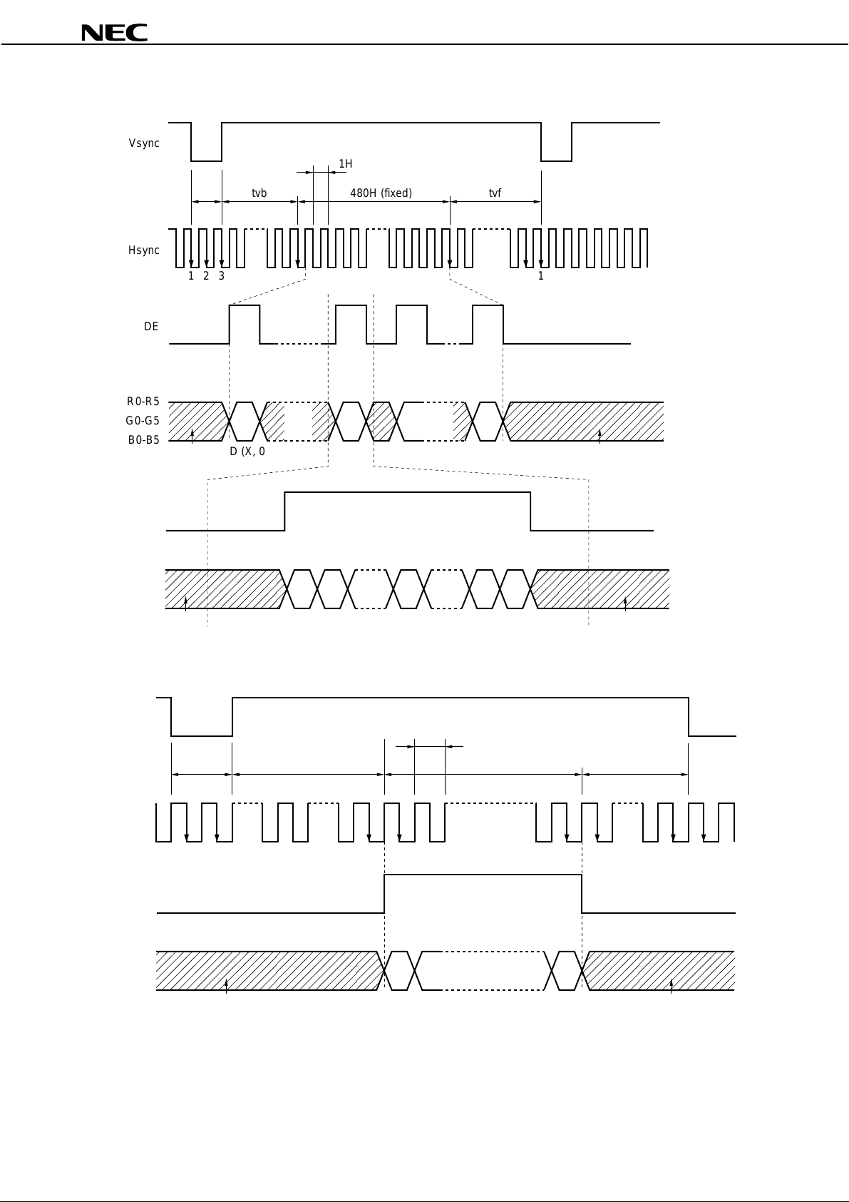
(b) DE mode
,,,,,,
Vsync
NL6448BC33-31
1H
Hsync
DE
R0-R5
G0-G5
B0-B5
DE
R0-R5
G0-G5
B0-B5
tvp
123 1
INVALID
INVALID
tvb 480H (fixed) tvf
D (X, 0) D (X, Y) D (X, 479)
D (0, Y)
D (1, Y) D (639, Y)
D (X, Y)
D (638, Y)
INVALID
(Note X = 0 to 639)
INVALID
Hsync
CLK
DE
R0-R5
G0-G5
B0-B5
1CLK
thp 640CLK (fixed) thf
12 1
INVALID
thb
D (0, Y)
D (1, Y)
D (639, Y)
INVALID
(Note Y = 0 to 479)
Data Sheet EN0443EJ1V0DS00
15
Page 16
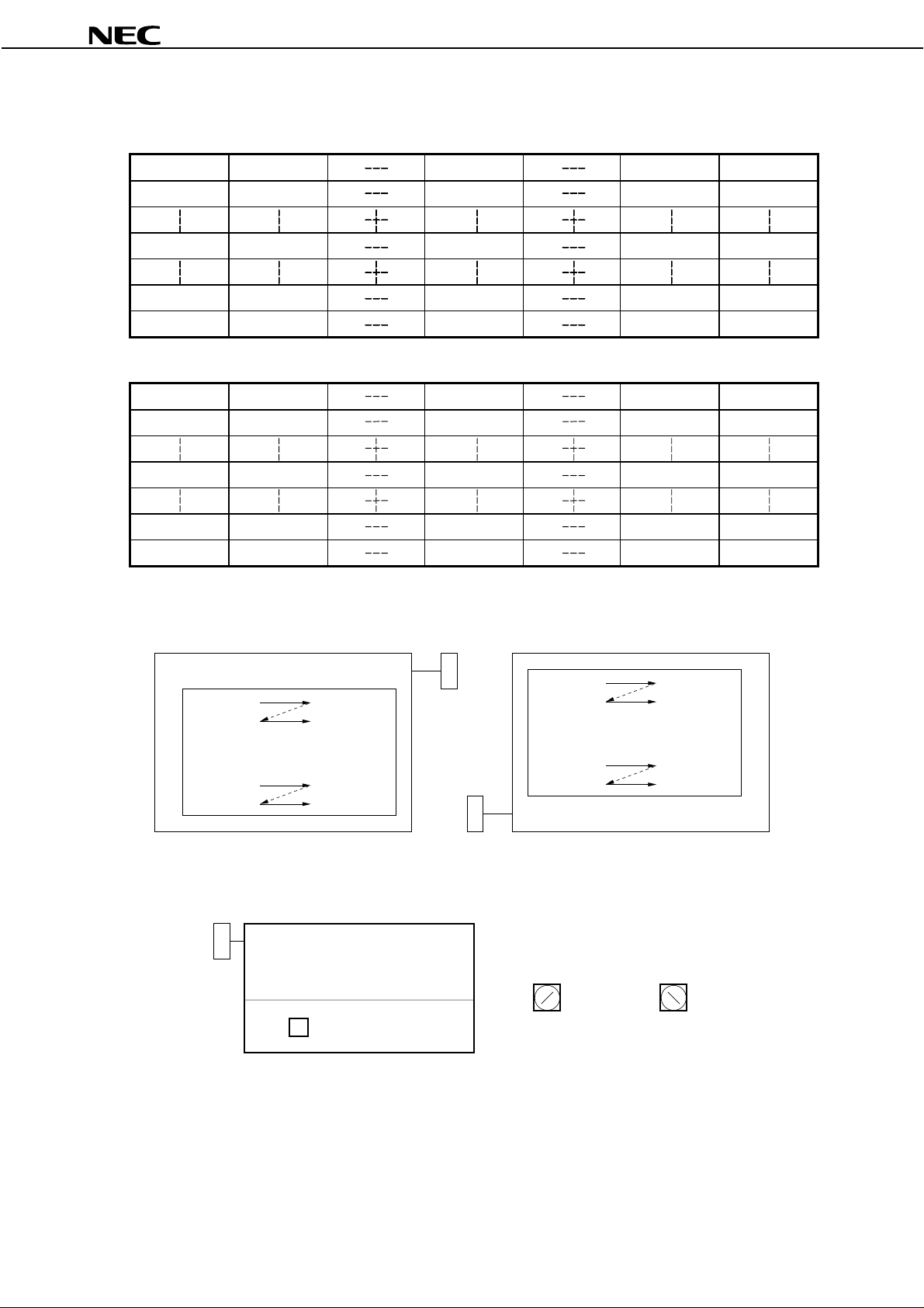
NL6448BC33-31
(4) Display position of input data
Normal scan (DPS = “GND” or “Open”)
D (0, 0) D (1, 0) D (X, 0) D (638, 0) D (639, 0)
D (0, 1) D (1, 1) D (X, 1) D (638, 1) D (639, 1)
D (0, Y) D (1, Y) D (X, Y) D (638, Y) D (639, Y)
D (0, 478) D (1, 478) D (X, 478) D (638, 478) D (639, 478)
D (0, 479) D (1, 479) D (X, 479) D (638, 479) D (639, 479)
Reverse scan (DPS = “VCC”)
D (639, 479) D (638, 479) D (X, 479) D (1, 479) D (0, 479)
D (639, 478) D (638, 478) D (X, 478) D (1, 478) D (0, 478)
D (639, Y) D (638, Y) D (X, Y) D (1, Y) D (0, Y)
D (639, 1) D (638, 1) D (X, 1) D (1, 1) D (0, 1)
D (639, 0) D (638, 0) D (X, 0) D (1, 0) D (0, 0)
Notes 1.
Below drawings show relations between the scan direction and the viewing direction.
Normal scan Reverse scan
C
N
2
D (0, 0) D (639, 0)
C
N
1
D (0, 479) D (639, 479)
When DPS is open or low, the scan direction is set up by the switch (SW1) on the rear side.
2.
Rear view
C
N
2
D (0, 0) D (639, 0)
D (0, 479) D (639, 479)
The scan direction select
C
N
1
16
SW1
Normal scan
(Factory set)
Reverse scan
See (1) Interface signals, power supply (Note 5) about another way for reversible scan.
When DPS is High, reverse scan is selected even if SW1 is set at normal scan.
Data Sheet EN0443EJ1V0DS00
Page 17
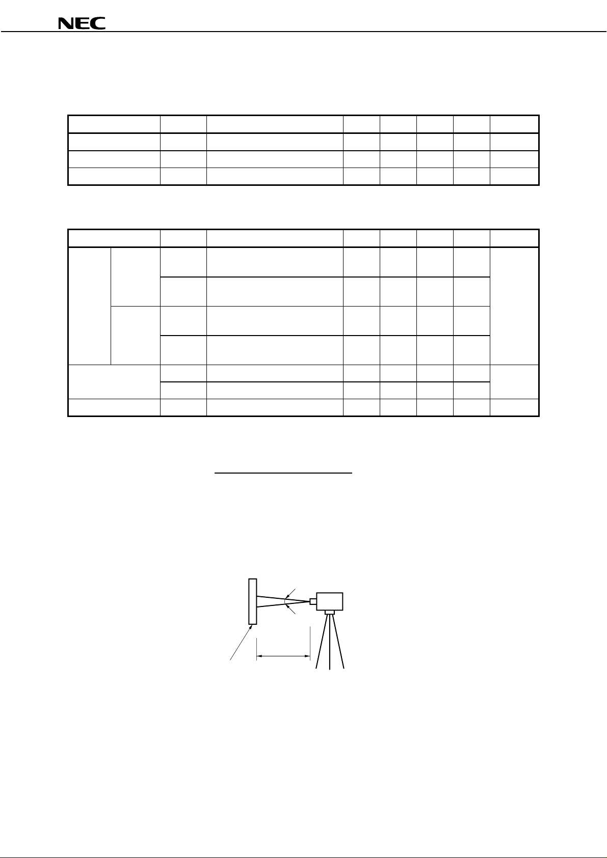
NL6448BC33-31
OPTICAL CHARACTERISTICS
Ta = 25 ± 5°C, VCC = 3.3 V VDDB = 12 V, MAV = VCC or open, at normal scan
Parameters Symbols Conditions MIN. TYP. MAX. Unit Remarks
Contrast ratio CR
Luminance L VMA XθX = ±0°, θY = ±0°, at center 280 350
Luminance uniformity
−
θ
X = ±0°, θY = ±0°, at center 150 300
max. /min.
−
1.25 1.40
−−
−
cd/m
−
Reference data
Parameters Symbols Conditions MIN. TYP. MAX. Unit Remarks
θ
Viewing
angle
range
Color gamut C At center. to NTSC 35 43
Horizontal
Vertical
X+ CR > 10, θY = ±0° (CR > 5) 45
−
θ
X
θ
Y+ CR > 10, θX = ±0° (CR > 5) 35
θ
Y
t on White to black
t off Black to white
CR > 10, θY = ±0° (CR > 5)
−
CR > 10, θX = ±0° (CR > 5) 40
−
45
−
−
−
−
−
50
(60)
50
(60)
40
(50)
45
(55)
15 40 msResponse time
70 85 ms
−
−
−
−
−
−
−
−
−
deg.
deg.
deg.
deg.
%
Note 1
2
Note 2
Note 3
Note 4
Note 5
−
Notes 1.
The contrast ratio is calculated by using the following formula.
Contrast ratio (CR) =
Luminance with all pixels in white
Luminance with all pixels in black
The Luminance is measured in darkroom.
The luminance is measured after 20 minutes from the module works, with all pixels in white. Typical
2.
value is measured after luminance saturation.
Photodetector
1°
(TOPCON BM-5A)
LCD
50 cm
Data Sheet EN0443EJ1V0DS00
17
Page 18
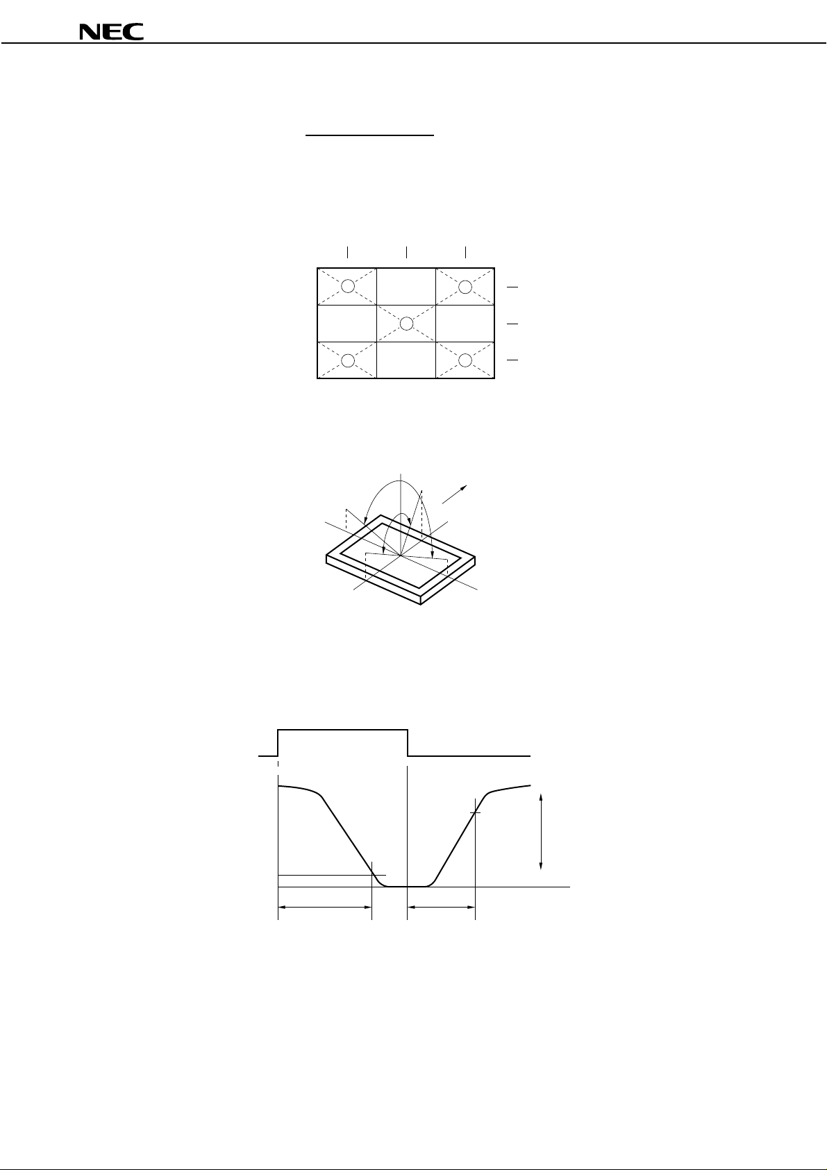
The luminance uniformity is calculated by using following formula.
3.
NL6448BC33-31
Luminance uniformity =
Maximum lumi nance
Minimum luminance
The luminance is measured at near the five points shown below.
Column
Definitions of viewing angle are as follows.
4.
106
1
4
320 533
2
3
5
The viewing angles are reference.
Normal
Left
X–
θ
θ
Y+
θ
Y–
θ
X+
12 o’clock
Upper
Line
80
240
400
Down
Definition of response time is as follows.
5.
Right
Photodetector output signal is measured when the luminance changes “White” to “Black” . Response
time (ton) is the time between 10% and 100% of the photodetector output amplitude. Response time
(toff) is the time between 0% and 90% of the output amplitude.
Data
100 %
90 %
Luminance
10 %
0 %
ton toff
On
Off
White
Display color
Black
Time
18
Data Sheet EN0443EJ1V0DS00
Page 19
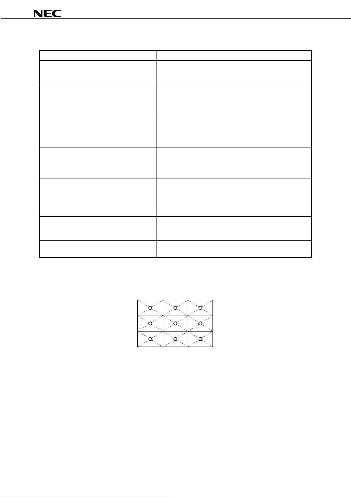
RELIABILITY TEST
Test items Test conditions
NL6448BC33-31
High temperature/humidity operation
Heat cycle (operation)
Thermal shock (non-operation)
Vibration (non-operation)
Mechanical shock (non-operation)
ESD (operation)
Dust (operation)
Note 1
Note 1
Notes 1, 2
Notes 1, 2
Notes 1, 3
Note 1
Note 1
50 ± 2°C, 85% relative humidity
240 hours
Display data is black.
<1> 0°C ± 3°C ··· 1 hour
55°C ± 3°C ··· 1 hour
<2> 50 cycles, 4 hours/cycle
<3> Display dat a is black.
<1> –20°C ± 3°C ··· 30 minutes
60°C ± 3°C ··· 30 minutes
<2> 100 cycles
<3> Temperature transition time within 5 minutes
<1> 5 - 100 Hz, 2G
1 minute/cycle
X, Y, Z direction
<2> 120 times each direction
<1> 55 G, 11 ms
X, Y direction
30G, 11 ms
Z direction
<2> 5 times each direction
150 pF, 150 Ω, ±10 kV
9 places on a panel
10 times each place at one-second intervals
15 kinds of dust (JIS Z 8901)
Hourly 15 seconds stir, 8 times repeat
Notes 1.
Display function is checked under the same condition as LCD module out-going inspection.
Physical damage.
2.
Discharge points “{” are shown in the figure.
3.
Data Sheet EN0443EJ1V0DS00
19
Page 20
GENERAL CAUTIONS
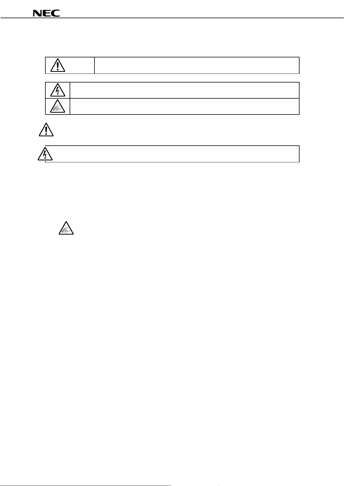
Next figures and sentence are very important. Please understand these contents as follows.
This figure is a mark that you will get hurt and/or the module will have damages when you make
CAUTION
This figure is a mark that you will get an electric shock when you make a mistake to operate.
This figure is a mark that you will get hurt when you make a mistake to operate
CAUTIONS
Do not touch an inverter, on which is stuck a caution label, while the LCD module is under the operation, because
of dangerous high voltage.
(1) Caution when taking out the module
a) Pick the pouch only, when taking out the module from a carrier box.
a mistake to operate.
NL6448BC33-31
(2) Cautions for handling the module
a) As the electrostatic discharges may break the LCD module, handle the LCD module with care against
electrostatic discharges.
b) As the LCD panel and backlight element are made from fragile glass material, impulse and
pressure to the LCD module should be avoided.
c) As the surface of polarizer is very soft and easily scratched, use a soft dry cloth without chemicals for
cleaning.
d) Do not pull the interface connectors in or out while the LCD module is operating.
e) Put the module display side down on a flat horizontal plane.
f) Handle connectors and cables with care.
g) When the module is operating, do not lose CLK, Hsync or Vsync signal. If any one or more of these signals
is lost, the LCD panel would be damaged.
h) The torque for mounting screws should never exceed 0.294 N·m (3 kgf·cm).
(3) Cautions for the atmosphere
a) Dew drop atmosphere must be avoided.
b) Do not store and/or operate the LCD module in high temperature and/or high humidity atmosphere.
Storage in an electro-conductive polymer packing pouch and under relatively low temperature atmosphere
is recommended.
c) This module uses cold cathod fluorescent lamps. Therefore, the life time of lamp becomes short
conspicuously at low temperature.
d) Do not operate the LCD module in high magnetic field.
(4) Cautions for the module characteristics
a) Do not apply any fixed patterns data signal for a long time to the LCD module at product aging. It may
cause image sticking.
b) This module has the retardation film which may cause the variation of color hue in the different viewing
angles. The ununiformity may appear on the screen under the high temperature operation.
20
Data Sheet EN0443EJ1V0DS00
Page 21

NL6448BC33-31
(5) Other cautions
a) Do not disassemble and/or reassemble LCD module.
b) Do not readjust variable resistors nor switches etc.
c) When returning the module for repair or etc, please pack the module not to be broken. We recommend the
original shipping packages.
Liquid Crystal Display has the following specific characteristics. There are not defects nor malfunctions.
• The display condition of the LCD module may be affected by the ambient temperature.
• The LCD module uses cold cathode tube for backlighting. Optical characteristics, like luminance or
uniformity, will change during time .
• Uneven brightness and/or small spots may be noticed depending on different display patterns.
Data Sheet EN0443EJ1V0DS00
21
Page 22
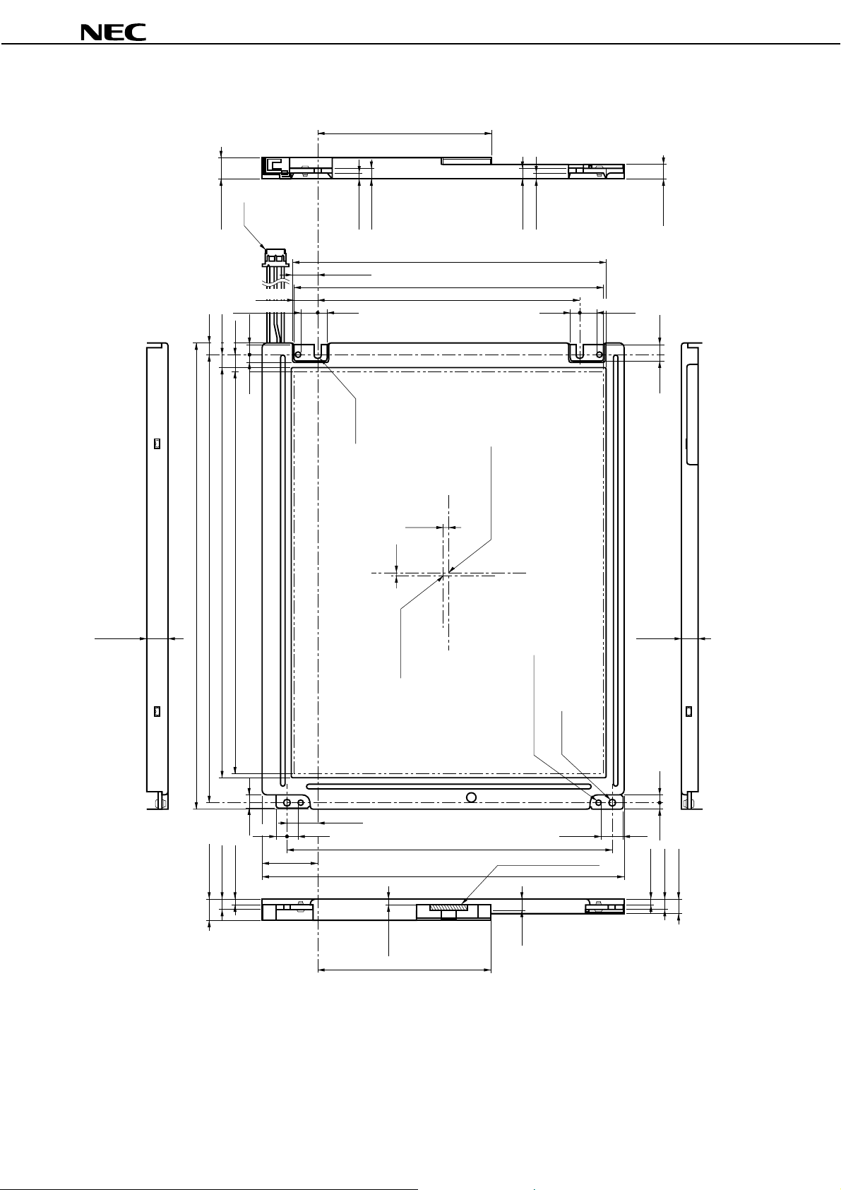
OUTLINE DRAWING: Front View (Unit: mm)
NL6448BC33-31
(88.3)
11.5MAX.
CN2
11.5MAX.
(12.9) 132.6±0.3
(8.1) (4.7)
(4.8)
(3.9)(2.9)
(9.3)
7.2±0.3
243±0.5
235±0.3
(211.2) (Active area)
(215.4) (Bezel opening)
14.6±0.3
2–R1.75
5.25±0.3
2.75±0.2
(161.8) (Bezel opening)
(158.4) (Active area)
(3.15)
(1.8)
5.25±0.3
2.75±0.2
(4.7)
Active area center
8.25TYP
(8.1)
(3.9)(2.9)
8.25TYP
5.25±0.3
2.75±0.2
11.5MAX.
(2.8) (4)
(5.7)
(29.4)
(5.1)
17±0.3
Module center
166.6±0.3
185.1±0.5
(3.7)
(88.3)
φ
2– 3.5
4–CPIMS × M2 × L4
(5.1)
CN1 : DF9C-31P-1V
Remark The torque to mounting screw
(6.3)
(5.7)
should never exceed 0.294 N·m
(3 kgf·cm).
2.75±0.2
(2.8) (4)
5.25±0.3
8.25TYP
22
Data Sheet EN0443EJ1V0DS00
Page 23
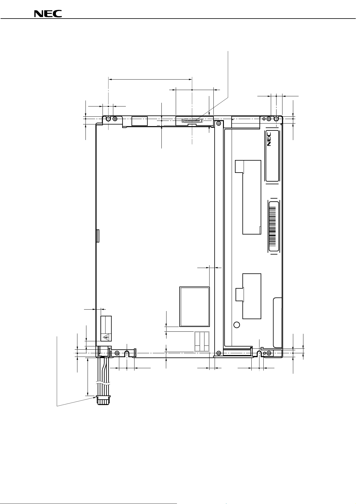
OUTLINE DRAWING: Rear View (Unit: mm)
(83.3)
(5)(5.3)
(2.4)(5.6)
(2.3)
(4.6)
(16.4) (21.6)
(10.1)
NL6448BC33-31
CN1 : DF9C-31P-1V
(5) (5.3)
(6.6) (2.4)
MADE IN JAPANDS2228423
A 2000A483324
NL6448BC33-31
(5)
CAUTION
(5)
NION VOLTEGE
(4.5)
(3.4)
60±10
BHR-03VS-1 (JST)
1PIN : COLD, 2-3PIN : HOT
RISK OF ELECTRIC SHOCK.
DISCONNECT THE ELECTRIC
POWER BEFORE SERVICE.
K2000A483324
(5)
(5)
THE TFT COLOR LCD
PANEL CONTAINS COLD CATHODE
FLOURESCENT LAMPS. PLEASE
FOLLOW LOCAL ORDINANCES
OR REGULATIONS FOR ITS
DISPOSAL
∗ ∗ ∗ − ∗
104DLM-
Pal No.
Name
S
(6.8)(8)
(5)
(5)
(6.8)
(5)
(4.5)
(3.4) (3.4)
Data Sheet EN0443EJ1V0DS00
23
Page 24
NL6448BC33-31
DATA SHEET
No part of this document may be copied or reproduced in any form or by any means without the prior written
consent of NEC Corporation. NEC Corporation assumes no responsibility for any errors which may appear in
this document.
NEC Corporation does not assume any liability for infringement of patents. Copyrights or other intellectual
property rights of third parties by or arising from use of a device de scribed h erein or any other liability arising from
use of such device. No license, either express, implied or otherwise, is granted under any patents, copyrights or
other intellectual property rights of NEC Corporation or others.
While NEC Corporation has been making continuous effort to enhance the reliability of its Electronic
Components, the possibility of defects cannot be eliminated entirely. To minimize risks of damage or injury to
persons or property arising from a defect in an NEC Electronic Components, customers must incorporate
sufficient safety measures in its design, such a s redundancy, fire-containment, and anti-failure features.
NEC devices are classified into the following three q uality grade s:
“Standard”, “Special”, and “Specific”. The Specific quality grade applies only to devices developed based on a
customer designated “quality assurance program” for a specific application. The recommended applications of a
device depend on its quality grade, as indicated below. Customers must check the quality grade of each device
before using it in a particular application.
Standard: Computers, office equipment, communications equipment, test and measurement equipment, audio
and visual equipment, home electronic appliances, machine tools, personal electronic equipment and industrial
robots
Special: Transportation equipment (automobiles, trains, ships, etc.), traffic control systems, anti-disaster
systems, anti-crime systems, safety equipment and m edica l equipment (not specifically designe d for life s upport)
Specific: Aircrafts, aerospace equipment, submersible repeaters, nuclear reactor control systems, life support
systems or medical equipment for life support, etc.
The quality grade of NEC devices is “Standard” unless otherwis e spe cified i n NEC ’s Data Sheets or D ata Books.
If customers intend to use NEC devices for applications other than those specified for Standard quality grade,
they should contact an NEC sales representative in adv ance.
Anti-radioactive design is not implemented in this produ ct.
 Loading...