

NJG1709KC1
- 1 -
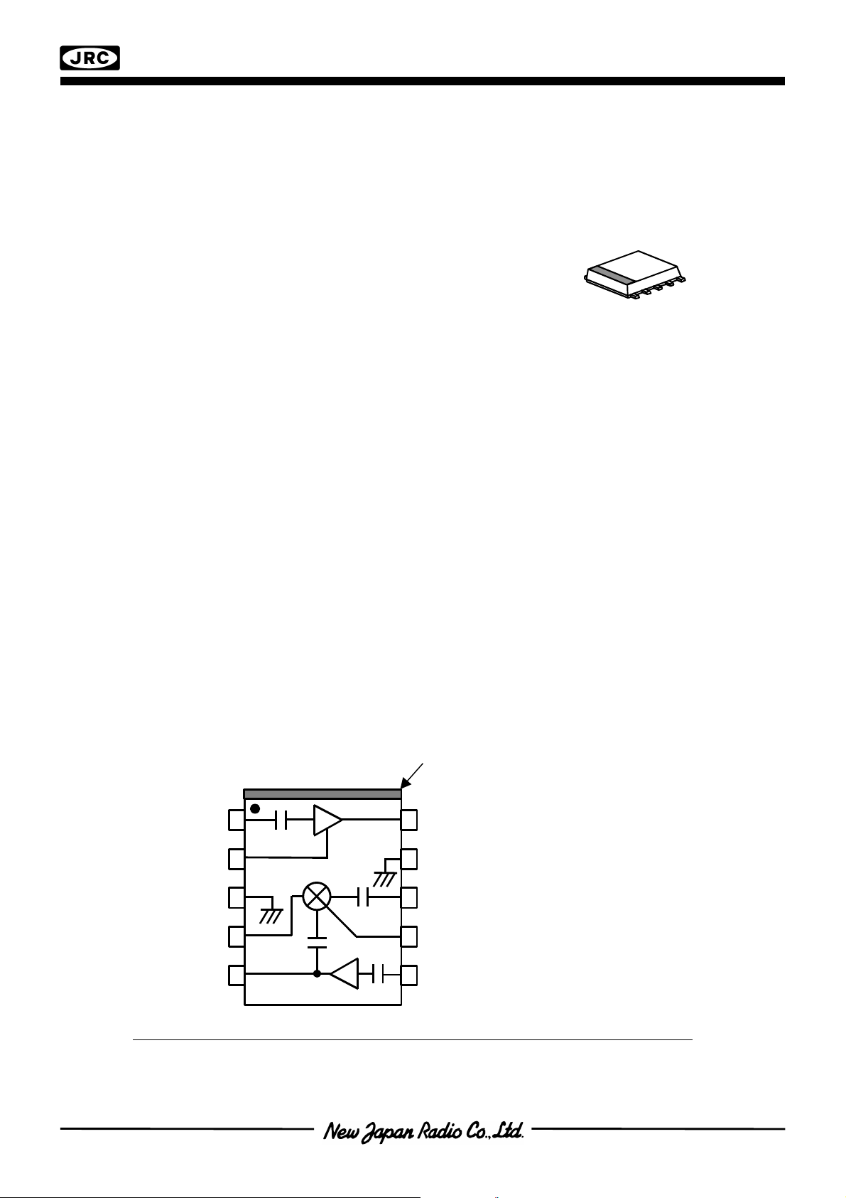
1.5/1.9GHz BAND FRONT-END GaAs MMIC
10.LNAOUT
KC1 Type
n
GENERAL DESCRIPTION
NJG1709KC1 is a front-end GaAs MMIC including a LNA,
a local amplifier and a mixer, designed mainly for 1.5 or
1.9GHz band cellular phone.
The ultra small & ultra thin FLP10 package is applied.
n
PACKAGE OUTLINE
n
FEATURES
lLow Voltage Operation +2.7V typ.
lLow Current Consumption LNA 3.2mA typ.
Mixer 5.1mA typ. (with Local Amplifier operation current)
lUltra Small & Ultra Thin package FLP10-C1 (Mount Size: 2.8 x 3.0 x 0.75mm)
LNA
lHigh Small Signal Gain 18.0dB typ. @ fRF=1489MHz
16.0dB typ. @ fRF=1900MHz
lLow Noise Figure 1.2dB typ. @ fRF=1489MHz
1.3dB typ. @ fRF=1900MHz
lHigh Output IP3 +13.0dBm typ. @ fRF=1489.0+1489.1MHz
+13.0dBm typ. @ fRF=1900.0+1900.1MHz
Mixer
lHigh Conversion Gain 12.5dB typ. @ fRF=1489MHz, fLO=1619MHz, PLO=-15dBm
9.0dB typ. @ fRF=1900MHz, fLO=1660MHz, PLO=-15dBm
lLow Noise Figure 6.0dB typ. @ fRF=1489MHz, fLO=1619MHz, PLO=-15dBm
6.5dB typ. @ fRF=1900MHz, fLO=1660MHz, PLO=-15dBm
lHigh Output IP3 +10.0dBm typ. @ fRF=1489.0+1489.1MHz, fLO=1619MHz, PLO=-15dBm
+11.0dBm typ. @ fRF=1900.0+1900.1MHz, fLO=1660MHz, PLO=-15dBm
NJG1709KC1
n
PIN CONFIGURATION
NOTE: Please note that any information on this catalog will be subject to change.
(Top View)
1
2
3
4
5 6
Orientation Mark
Pin Connection
10
9
8
7
1.LNAIN
2.LNACAP
3.GND
4.IFOUT
5.VLO
6.LOIN
7.BPC
8.MIXIN
9.GND
NJG1709KC1
- 2 -
n
M
ABSOLUTE MAXIMUM RATINGS
(Ta=+25°C, Zs=Zl=50Ω)
PARAMETER SYMBOL CONDITIONS RATINGS UNITS
LNA Voltage V
Mixer Voltage V
Local Amplifier Voltage V
Input Power 1 P
Input Power 2 P
Power Dissipation P
Operating Temperature T
Storage Temperature T
n
ELECTRICAL CHARACTERISTICS 1 (LNA)
LNA
MIX
LO
LNAIN
LOIN
D
opr
stg
GENERAL CONDITIONS: Ta=+25°C, V
V
LNA=VMIX=VLO
V
LNA=VMIX=VLO
LNA
=2.7V +15 dBm
=2.7V +10 dBm
=2.7V, V
MIX=VLO
=0V, fRF=1489MHz, PRF=-36dBm,
5.0 V
5.0 V
5.0 V
550 mW
-40~+85 °C
-55~+125 °C
Zs=Zl=50Ω, with test circuit 1
PARAMETER SYMBOL CONDITIONS MIN TYP MAX UNITS
Operating Frequency freq 1470 1489 1510 MHz
LNA Voltage V
LNA Operating Current I
LNA
LNA
PRF, PLO=OFF - 3.2 4.1 mA
2.5 2.7 4.5 V
Small Signal Gain Gain 16.0 18.0 20.0 dB
Gain Flatness G
flat
fRF=1470~1520MHz - 0.5 1.0 dB
Noise Figure NF - 1.2 1.5 dB
Pout at 1dB Gain
Compression point
Output 3rd order
Intercept point
RF IN VSWR VSWR
RF OUT VSWR VSWR
P
-1dB
-3.0 -1.0 - dBm
OIP3 fRF=1489.0+1489.1MHz +8.0 +13.0 - dBm
i
o
- 1.5 -
- 1.5 -
n
ELECTRICAL CHARACTERISTICS 2 (Mixer)
GENERAL CONDITIONS: Ta=+25°C, V
LNA
=0V, V
MIX=VLO
=2.7V, fRF=1489MHz, fLO=1619MHz
PRF=-30dBm, PLO=-15dBm, Zs=Zl=50Ω, with test circuit 1
PARAMETER SYMBOL CONDITIONS MIN TYP MAX UNITS
Operating Frequency freq 1470 1489 1510 MHz
Mixer Voltage V
Local Amplifier Voltage V
Mixer Operating Current I
Local Amplifier
Operating Current
I
Conversion Gain G
MIX
LO
MIX
LO
PRF, PLO=OFF - 4.3 5.7 mA
PRF, PLO=OFF - 0.8 1.3 mA
c
2.5 2.7 4.5 V
2.5 2.7 4.5 V
11.0 12.5 - dB
Noise Figure NF - 6.0 9.0 dB
Output 3rd Order
Intercept Point
MIXER IN VSWR VSWR
LOCAL IN VSWR VSWR
IF OUT VSWR VSWR
OIP3 fRF=1489.0+1489.1MHz +7.0 +10.0 - dBm
- 1.5 -
L
I
- 1.5 -
- 1.5 -
NJG1709KC1
- 3-
n
ELECTRICAL CHARACTERISTICS 3 (LNA)
GENERAL CONDITIONS: Ta=+25°C, V
=2.7V, V
LNA
MIX=VLO
=0V, fRF=1900MHz, PRF=-36dBm,
Zs=Zl=50Ω, with test circuit 2
PARAMETER SYMBOL CONDITIONS MIN TYP MAX UNITS
Operating Frequency freq 1890 1900 1920 MHz
LNA Voltage V
LNA Operating Current I
LNA
LNA
PRF, PLO=OFF - 3.2 4.1 mA
2.5 2.7 4.5 V
Small Signal Gain Gain 14.0 16.0 18.0 dB
Gain Flatness G
flat
fRF=1890∼1920MHz
- 0.5 1.0 dB
Noise Figure NF - 1.3 1.5 dB
Pout at 1dB Gain
Compression point
Output 3rd Order
Intercept point
RF IN VSWR VSWR
RF OUT VSWR VSWR
n
ELECTRICAL CHARACTERISTICS 4 (Mixer)
GENERAL CONDITIONS: Ta=+25°C, V
P
-1dB
-2.0 0 - dBm
OIP3 fRF=1900.0+1900.1MHz +9.0 +13.0 - dBm
i
o
LNA
=0V, V
MIX=VLO
=2.7V, fRF=1900MHz, fLO=1660MHz
- 2.0 -
- 2.0 -
PRF=-30dBm, PLO=-15dBm, Zs=Zl=50Ω, with test circuit 2
PARAMETER SYMBOL CONDITIONS MIN TYP MAX UNITS
Operating Frequency freq 1890 1900 1920 MHz
Mixer Voltage V
Local Amplifier Voltage V
Mixer Operating Current I
Local Amplifier
Operating Current
I
Conversion Gain G
MIX
MIX
LO
LO
PRF, PLO=OFF - 4.3 5.7 mA
PRF, PLO=OFF - 0.8 1.3 mA
c
2.5 2.7 4.5 V
2.5 2.7 4.5 V
7.0 9.0 - dB
Noise Figure NF - 6.5 9.0 dB
Output 3rd Order
Intercept point
MIXER IN VSWR VSWR
LOCAL IN VSWR VSWR
IF OUT VSWR VSWR
OIP3 fRF=1900.0+1900.1MHz +7.0 +11.0 - dBm
M
L
I
- 1.5 -
- 1.5 -
- 1.5 -

NJG1709KC1
- 4 -
n
TERMINAL INFORMATION
No. SYMBOL FUNCTION
1 LNAIN RF input terminal of LNA. An external matching circuit is required.
2 LNACAP
3 GND Ground terminal (0V)
4 IFOUT
5 VLO
6 LOIN
7 BPC
8 MIXIN RF signal input terminal to mixer. An external matching circuit is required.
9 GND Ground terminal (0V)
10 LNAOUT
Terminal for the bypass capacitor of LNA. The bypass capacitor C1 shown
in test circuits should be connected to this terminal as close as possible.
IF signal output terminal. The IF signal is output through external matching
circuit connected to this terminal. Please connect inductances L7, L8 and
power supply as shown in test circuits, since this terminal is also the terminal
of mixer power supply.
Power supply terminal for local amplifier. Please place R1, R2 and L11
shown in test circuits at very close to this terminal.
Local signal input terminal to local amplifier. An external matching circuit is
required.
Terminal for the bypass capacitor of mixer. The bypass capacitor C4 shown
in test circuits should be connected to this terminal as close as possible.
Signal output terminal of LNA. The RF signal from LNA goes out through
external matching circuit connected to this terminal. Please connect
inductances L3, L4 and power supply as shown in test circuits, since this
terminal is also the terminal of LNA power supply.
CAUTION
1) Ground terminal (No.3, 9) should be connected to the ground plane as close as possible.

NJG1709KC1
- 5-
n
LNA
LNA
LNA
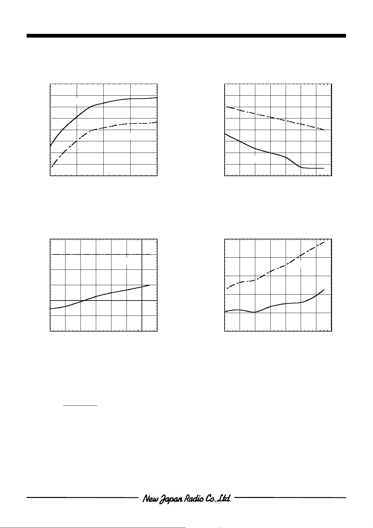
TYPICAL CHARACTERISTICS 1 (LNA, f=1.5GHz, fLO=1619MHz, with test circuit 1)
Gain, NF vs. Frequency
(V
=2.7V)
19
18
17
LNA
Gain
16
15
Gain (dB)
14
13
12
1450 1460 1470 1480 1490 1500 1510 1520 1530
NF
Frequency (MHz)
Pout, IM3 vs. Pin
(V
=2.7V, f=1489+1489.1MHz)
20
0
LNA
4
3.5
3
2.5
2
1.5
Noise Figure (dB)
1
0.5
Pout vs. Pin
(V
=2.7V, f=1489MHz)
10
5
0
-5
-10
Pout (dBm)
-15
-20
-25
-40 -35 -30 -25 -20 -15 -10 -5 0
18
17.5
LNA
Pin (dBm)
Gain, NF vs. V
(f=1489MHz)
Gain
LNA
2
-20
-40
-60
Pout,IM3 (dBm)
-80
-100
-40 -35 -30 -25 -20 -15 -10 -5 0
Pout
IM3
Pin (dBm)
I
vs. V
LNA
3.8
3.7
3.6
LNA
(mA)
LNA
3.5
I
3.4
17
16.5
Gain (dB)
16
NF
15.5
15
2.5 3 3.5 4 4.5
V
(V)
P-1dB vs. V
LNA
(f=1489MHz)
8
6
4
2
0
-2
P-1dB (dBm)
-4
-6
1.5
1
Noise Figure (dB)
0.5
3.3
2.5 3 3.5 4 4.5
V
(V)
-8
2.5 3 3.5 4 4.5
V
(V)
NJG1709KC1
- 6 -
n
LNA
TYPICAL CHARACTERISTICS 1 (LNA, f=1.5GHz, fLO=1619MHz, with test circuit 1)
OIP3, IIP3 vs. V
LNA
(f=1489+1489.1MHz,Pin=-36dBm)
21
19
OIP3
17
15
13
11
OIP3 (dBm)
9
7
5
2.5 3 3.5 4 4.5
V
IIP3
(V)
NF,P-1dB vs. Temperature
(V
=2.7V,f=1489MHz)
3
LNA
8
6
4
2
0
-2
-4
-6
-8
0
IIP3 (dBm)
20
19.5
19
18.5
18
Gain (dB)
17.5
17
Gain, I
vs. Temperature
LNA
(V
=2.7V, f=1489MHz)
LNA
I
LNA
Gain
16.5
16
-40 -20 0 20 40 60 80 100
Ambient Temperature (oC)
OIP3,IIP3 vs. Temperature
(V
=2.7V,f=1489+1489.1MHz,Pin=-36dBm)
LNA
16
3.8
3.7
3.6
3.5
3.4
3.3
3.2
3.1
3
-3
(mA)
LNA
I
2.5
P-1dB
2
1.5
NF (dB)
1
0.5
0
-40 -20 0 20 40 60 80 100
NF
Ambient Temperature (oC)
The value of OIP3 and IIP3 shown in
typical characteristics are calculated
3×Pout−IM3
OIP3=
2
IIP3=OIP3-Gain @Pin=-36dBm
-1
-2
-3
-4
-5
-6
P-1dB (dBm)
15
IIP3
14
13
OIP3 (dBm)
12
OIP3
11
-40 -20 0 20 40 60 80 100
Ambient Temperature (oC)
-4
-5
-6
-7
-8
IIP3 (dBm)
NJG1709KC1
- 7-
n
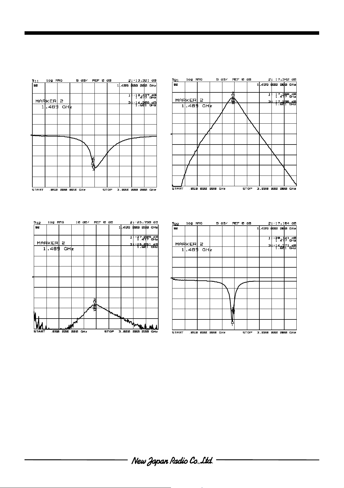
TYPICAL CHARACTERISTICS 1 (LNA, f=1.5GHz, fLO=1619MHz, with test circuit 1)
S11
S12
Condition
V
=2.7V
LNA
V
MIX=VLO
S21
S22
=0V
NJG1709KC1
- 8 -
n
TYPICAL CHARACTERISTICS 1 (MIXER, f=1.5GHz, fLO=1619MHz, with test circuit 1)
Conversion Gain, Noise Figure
vs. RF Frequency
16
14
12
10
8
Conversion Gain (dB)
6
1450 1460 1470 1480 1490 1500 1510 1520 1530
Gc
RF Frequency (MHz)
Condition
fIF=130MHz
PRF=-30dBm
PLO=-15dBm
V
MIX=VLO
Upper LOCAL
NF
=2.7V
14
12
10
8
Noise Figure (dB)
6
4
Conversion Gain, Noise Figure
vs. LO Power
20
15
10
5
Gc
0
Conversion Gain (dB)
-5
-40 -30 -20 -10 0 10
LO Power (dBm)
Condition
fIF=130MHz
fRF=1489MHz, PRF=-30dBm
fLO=1619MHz
V
MIX=VLO
=2.7V
NF
12
10
8
6
Noise Figure (dB)
4
2
OIP3, IIP3 vs. LO Power
15
10
5
OIP3
0
OIP3 (dBm)
-5
-10
-40 -30 -20 -10 0 10
LO Power (dBm)
Condition
fIF=130MHz
f
=1489.0MHz, PRF=-30dBm
RF1
f
=1489.1MHz
RF2
fLO=1619MHz
V
MIX=VLO
=2.7V
IIP3
OIP3=
IIP3=OIP3-Gc
@ PRF =-30dBm
3×IF−IM3
2
0
-5
-10
-15
-20
-25
IIP3 (dBm)
NJG1709KC1
- 9-
n
MIX
MIX
TYPICAL CHARACTERISTICS 1 (MIXER, f=1.5GHz, fLO=1619MHz, with test circuit 1)
Conversion Gain, Noise Figure
OIP3, IIP3 vs. V
15
14
Gc
vs. V
MIX
, V
LO
10
9
16
14
MIX
, V
IIP3
LO
0
-2
13
12
11
Conversion Gain (dB)
10
2.5 3 3.5 4 4.5
V
, VLO (V)
NF
Condition
fIF=130MHz
fRF=1489MHz, PRF=-30dBm
fLO=1619MHz, PLO=-15dBm
IF, IM3 vs. RF Power
20
8
7
Noise Figure (dB)
6
5
12
10
OIP3 (dBm)
8
6
2.5 3 3.5 4 4.5
OIP3
V
, VLO (V)
Condition
fIF=130MHz
f
=1489.0MHz, PRF=-30dBm
RF1
f
=1489.1MHz
RF2
fLO=1619MHz, PLO=-15dBm
OIP3=
IIP3=OIP3-Gc
@ PRF =-30dBm
IF Output Power vs. RF Power
5
3×IF−IM3
2
-4
-6
-8
-10
IIP3 (dBm)
0
IF
-20
-40
-60
IF,IM3 (dBm)
IM3
-80
-100
-40 -35 -30 -25 -20 -15 -10 -5 0
RF Power (dBm)
Condition
fIF=130MHz
f
=1489.0MHz
RF1
f
=1489.1MHz
RF2
fLO=1619MHz, PLO=-15dBm
V
MIX=VLO
=2.7V
0
-5
-10
-15
-20
IF Output Power (dBm)
-25
-30
-40 -35 -30 -25 -20 -15 -10 -5 0
RF Power (dBm)
Condition
fIF=130MHz
fRF=1489MHz
fLO=1619MHz, PLO=-15dBm
V
MIX=VLO
=2.7V

NJG1709KC1
- 10 -
n
TYPICAL CHARACTERISTICS 1 (MIXER, f=1.5GHz, fLO=1619MHz, with test circuit 1)
Conversion Gain vs. LO Power
Temperature Response
15
10
5
Conversion Gain (dB)
0
-40 -30 -20 -10 0 10
LO Power (dBm)
Condition
fIF=130MHz
fRF=1489MHz, PRF=-30dBm
fLO=1619MHz
V
MIX=VLO
=2.7V
-40oC
-20oC
0oC
+20oC
+40oC
+60oC
+90oC
Noise Figure vs. LO Power
Temperature Response
15
10
5
Noise Fugure (dB)
0
-40 -30 -20 -10 0 10
LO Power (dBm)
Condition
fIF=130MHz
fRF=1489MHz
fLO=1619MHz
V
MIX=VLO
=2.7V
-40oC
-20oC
0oC
+20oC
+40oC
+60oC
+90oC
IIP3 vs. LO Power
Temperature Response
2
0
-2
-4
IIP3 (dBm)
-6
-8
-10
-40 -30 -20 -10 0 10
Condition
fIF=130MHz
f
=1489.0MHz, PRF=-30dBm
RF1
f
=1489.1MHz
RF2
fLO=1619MHz
V
MIX=VLO
-40oC
-20oC
0oC
+20oC
+40oC
+60oC
+90oC
LO Power (dBm)
=2.7V
IIP3=
@ PRF =-30dBm
3×IF−IM3
2
−Gc

NJG1709KC1
- 11-
n
MIX
MIX
MIX
TYPICAL CHARACTERISTICS 1 (MIXER, f=1.5GHz, fLO=1619MHz, with test circuit 1)
Conversion Gain vs. V
15
14
13
12
11
Conversion Gain (dB)
10
9
Temperature Response
2.5 3 3.5 4 4.5
V
, VLO (V)
MIX
Condition
fIF=130MHz
fRF=1489MHz,PRF=-30dBm
fLO=1619MHz, PLO=-15dBm
, V
-40oC
-20oC
0oC
+20oC
+40oC
+60oC
+90oC
LO
Noise Figure vs. V
MIX
, V
Temperature Response
9
8
7
6
5
4
Noise Figure (dB)
3
2
2.5 3 3.5 4 4.5
V
, VLO (V)
Condition
fIF=130MHz
fRF=1489MHz
fLO=1619MHz, PLO=-15dBm
LO
-40oC
-20oC
0oC
+20oC
+40oC
+60oC
+90oC
IIP3 vs. V
MIX
, V
LO
Temperature Response
0
-1
-2
-3
-4
-5
IIP3 (dBm)
-6
-7
-8
2.5 3 3.5 4 4.5
V
, VLO (V)
Condition
fIF=130MHz
f
=1489.0MHz,PRF=-30dBm
RF1
f
=1489.1MHz
RF2
fLO=1619MHz, PLO=-15dBm
IIP3=
@ PRF =-30dBm
-40oC
-20oC
0oC
+20oC
+40oC
+60oC
+90oC
3×IF−IM3
2
-Gc

NJG1709KC1
- 12 -
n
TYPICAL CHARACTERISTICS 1 (MIXER, f=1.5GHz, fLO=1619MHz, with test circuit 1)
MIXER IN PORT IMPEDANCE
(PLO=-15dBm)
Condition
V
=0V
LNA
V
MIX=VLO
=2.7V
LOCAL IN PORT IMPEDANCE
Condition
V
=0V
LNA
V
MIX=VLO
=2.7V
IF OUT PORT IMPEDANCE
Condition
V
=0V
LNA
V
MIX=VLO
=2.7V

NJG1709KC1
- 13-
n
TYPICAL CHARACTERISTICS 1 (LNA+MIXER, f=1.5GHz, fLO=1619MHz, with test circuit 1)
RF IN – LOCAL IN ISOLATION
(RF IN → LOCAL IN)
Port 1
RF OUT – MIXER IN ISOLATION
(RF OUT → MIXER IN)
Condition
V
=2.7V
LNA
V
Port1:RF IN
Port2:LOCAL IN
Condition
V
V
Port1:RF OUT
Port2:MIXER IN
MIX=VLO
=2.7V
LNA
MIX=VLO
=2.7V
=2.7V
RF IN
IF OUT
50Ω
RF IN
50Ω
IF OUT
M.N
M.N.
RF OUT – MIXER IN
Coaxial Cable
Z0=50 ohm, L=260 mm
M.N
M.N.
50Ω
M.N
M.N.
M.N.
LOCAL IN
Port 2
M.N
M.N.
M.N.
LOCAL IN
RF OUT
MIXER IN
Port 1
RF OUT
MIXER IN
Port 2
RF IN – IF OUT ISOLATION
(RF IN → IF OUT)
Condition
V
=2.7V
LNA
V
MIX=VLO
Port1:RF IN
Port2:IF OUT
=2.7V
Port 1
RF IN
M.N
IF OUT
M.N.
Port 2
RF OUT – MIXER IN
Coaxial Cable
Z0=50 ohm, L=260 mm
50Ω
RF OUT
M.N
M.N.
MIXER IN
M.N.
LOCAL IN
50Ω

NJG1709KC1
- 14 -
n
TYPICAL CHARACTERISTICS 1 (LNA+MIXER, f=1.5GHz, fLO=1619MHz, with test circuit 1)
LOCAL IN to IF OUT Isolation
0
vs. LO Frequency
-5
-10
-15
-20
Isolation (dB)
-25
-30
1590 1600 1610 1620 1630 1640 1650
LO Frequency (MHz)
LOCAL IN to RF IN Isolation
vs. LO Frequency
0
-5
-10
-15
-20
Isolation (dB)
-25
-30
1590 1600 1610 1620 1630 1640 1650
LO Frequency (MHz)
Condition
V
=2.7V
LNA
V
MIX=VLO
=2.7V
PLO=-15dBm
Port1: LOCAL IN
Port2: IF OUT
Condition
V
=2.7V
LNA
V
MIX=VLO
=2.7V
PLO=-15dBm
Port1: LOCAL IN
Port2: RF IN
RF IN
50Ω
IF OUT
Port 2
Port 2
RF IN
IF OUT
M.N
M.N.
M.N.
LOCAL IN
Port 1
RF OUT – MIXER IN
Coaxial Cable
Z0=50 ohm, L=260 mm
M.N
M.N.
50Ω
M.N.
LOCAL IN
Port 1
RF OUT – MIXER IN
Coaxial Cable
Z0=50 ohm, L=260 mm
RF OUT
M.N
M.N.
MIXER IN
RF OUT
M.N
M.N.
MIXER IN

NJG1709KC1
- 15-
n
LNA
TYPICAL CHARACTERISTICS 2 (LNA, f=1.9GHz, fLO=1660MHz, with test circuit 2)
Gain, NF vs. Frequency
(VDD=2.7V)
19
18
17
Gain
16
15
Gain (dB)
14
13
12
1870 1880 1890 1900 1910 1920 1930 1940
NF
Frequency (MHz)
Pout , IM3 vs. Pin
(V
=2.7V, f=1900.0+1900.1MHz)
20
0
-20
LNA
Pout
4
3.5
3
2.5
2
1.5
Noise Figure (dB)
1
0.5
Pout vs. Pin
(V
=2.7V, f=1900MHz)
10
5
0
-5
-10
Pout (dBm)
-15
-20
-25
-40 -35 -30 -25 -20 -15 -10 -5 0
17
16.5
16
LNA
Pin (dBm)
Gain, NF vs. V
(f=1900MHz)
Gain
LNA
2
1.5
-40
-60
Pout, IM3 (dBm)
-80
-100
-40 -35 -30 -25 -20 -15 -10 -5 0
3.8
3.7
3.6
(mA)
LNA
3.5
I
3.4
IM3
Pin (dBm)
I
vs. V
LNA
LNA
15.5
Gain (dB)
15
14.5
14
2.5 3 3.5 4 4.5
V
P-1dB vs. V
NF
(V)
LNA
(f=1900MHz)
8
6
4
2
0
-2
P-1dB (dBm)
-4
-6
1
Noise Figure (dB)
0.5
3.3
2.5 3 3.5 4 4.5
V
(V)
LNA
-8
2.5 3 3.5 4 4.5
V
(V)
LNA

NJG1709KC1
- 16 -
n
The value of OIP3 and IIP3 shown in typical
TYPICAL CHARACTERISTICS 2 (LNA, f=1.9GHz, fLO=1660MHz, with test circuit 2)
OIP3 , IIP3 vs. V
LNA
(f=1900.0+1900.1MHz,Pin=-36dBm)
21
19
OIP3
17
15
IIP3
13
11
OIP3 (dBm)
9
7
5
2.5 3 3.5 4 4.5
V
(V)
LNA
NF,P-1dB vs. Temperature
(V
=2.7V, f=1900MHz)
3
LNA
8
6
4
2
0
-2
-4
-6
-8
1
IIP3 (dBm)
19
18.5
18
17.5
17
Gain (dB)
16.5
Gain, I
(V
vs. Temperature
LNA
=2.7V, f=1900MHz)
LNA
I
LNA
Gain
16
15.5
15
-40 -20 0 20 40 60 80 100
Ambient Temperature (oC)
OIP3,IIP3 vs. Temperature
(V
=2.7V, f=1900.0+1900.1MHz,Pin=-36dBm)
LNA
16
3.8
3.7
3.6
3.5
3.4
3.3
3.2
3.1
3
-2
(mA)
LNA
I
2.5
2
1.5
NF (dB)
1
0.5
0
-40 -20 0 20 40 60 80 100
NF
P-1dB
Ambient Temperature (oC)
characteristics are calculated
3×Pout−IM3
OIP3=
2
IIP3=OIP3-Gain @Pin=-36dBm
0
-1
-2
-3
-4
-5
P-1dB (dBm)
15
IIP3
14
13
OIP3 (dBm)
12
11
-40 -20 0 20 40 60 80 100
OIP3
Ambient Temperature (oC)
-3
-4
-5
-6
-7
IIP3 (dBm)

NJG1709KC1
- 17-
n
TYPICAL CHARACTERISTICS 2 (LNA, f=1.9GHz, fLO=1660MHz, with test circuit 2)
S11
S12
Condition
V
=2.7V
LNA
V
MIX=VLO
S21
S22
=0V

NJG1709KC1
- 18 -
n
TYPICAL CHARACTERISTICS 2 (MIXER, f=1.9GHz, fLO=1660MHz, with test circuit 2)
Conversion Gain, Noise Figure
vs. RF Frequency
12
10
8
6
Conversion Gain (dB)
4
2
1870 1880 1890 1900 1910 1920 1930 1940
Gc
RF Frequency (MHz)
Condition
fIF=240MHz
PRF=-30dBm
PLO=-15dBm
V
MIX=VLO
=2.7V
Upper LOCAL
NF
14
12
10
8
Noise Figure (dB)
6
4
Conversion Gain, Noise Figure
vs. LO Power
15
10
5
Gc
0
-5
Conversion Gain (dB)
-10
-40 -30 -20 -10 0 10
LO Power (dBm)
Condition
fIF=240MHz
fRF=1900MHz, PRF=-30dBm
fLO=1660MHz
V
MIX=VLO
=2.7V
NF
12
10
8
6
Noise Figure (dB)
4
2
OIP3 , IIP3 vs. LO Power
15
10
OIP3
5
0
OIP3 (dBm)
-5
-10
-40 -30 -20 -10 0 10
LO Power (dBm)
Condition
fIF=240MHz
f
=1900.0MHz, PRF=-30dBm
RF1
f
=1900.1MHz
RF2
fLO=1660MHz
V
MIX=VLO
=2.7V
IIP3
OIP3=
IIP3=OIP3-Gc
@ PRF =-30dBm
3×IF−IM3
2
15
10
5
0
-5
-10
IIP3 (dBm)

NJG1709KC1
- 19-
n
MIX
TYPICAL CHARACTERISTICS 2 (MIXER, f=1.9GHz, fLO=1660MHz, with test circuit 2)
Conversion Gain, Noise Figure
vs. V
12
11
Gc
10
9
8
Conversion Gain (dB)
7
2.5 3.0 3.5 4.0 4.5
V
Condition
fIF=240MHz
fRF=1900MHz, PRF=-30dBm
fLO=1660MHz, PLO=-15dBm
, V
MIX
, VLO (V)
LO
NF
10
9
8
7
Noise Figure (dB)
6
5
OIP3 , IIP3 vs. V
16
14
12
MIX
OIP3
10
OIP3 (dBm)
8
6
2.5 3 3.5 4 4.5
V
, VLO (V)
MIX
Condition
fIF=240MHz
f
=1900.0MHz, PRF=-30dBm
RF1
f
=1900.1MHz
RF2
fLO=1660MHz, PLO=-15dBm
OIP3=
IIP3=OIP3-Gc
@ PRF =-30dBm
, V
IIP3
LO
3×IF−IM3
2
4
2
0
-2
-4
-6
IIP3 (dBm)
IF , IM3 vs. RF Power
20
0
IF
-20
-40
-60
IF , IM3 (dBm)
IM3
-80
-100
-40 -35 -30 -25 -20 -15 -10 -5 0
RF Power (dBm)
Condition
fIF=240MHz
f
=1900.0MHz
RF1
f
=1900.1MHz
RF2
fLO=1660MHz, PLO=-15dBm
V
MIX=VLO
=2.7V
IF Output Power vs. RF Power
5
0
-5
-10
-15
-20
IF Output Power (dBm)
-25
-30
-40 -35 -30 -25 -20 -15 -10 -5 0
RF Power (dBm)
Condition
fIF=240MHz
fRF=1900MHz
fLO=1660MHz, PLO=-15dBm
V
MIX=VLO
=2.7V

NJG1709KC1
- 20 -
n
TYPICAL CHARACTERISTICS 2 (MIXER, f=1.9GHz, fLO=1660MHz, with test circuit 2)
Conversion Gain vs. LO Power
Temperature Response
15
10
5
Conversion Gain (dB)
0
-40 -30 -20 -10 0 10
LO Power (dBm)
Condition
fIF=240MHz
fRF=1900MHz, PRF=-30dBm
fLO=1660MHz
V
MIX=VLO
=2.7V
-40oC
-20oC
0oC
+20oC
+40oC
+60oC
+90oC
Noise Figure vs. LO Power
Temperature Response
15
10
5
Noise Figure (dB)
0
-40 -30 -20 -10 0 10
LO Power(dBm)
Condition
fIF=240MHz
fRF=1900MHz
fLO=1660MHz
V
MIX=VLO
=2.7V
-40oC
-20oC
0oC
+20oC
+40oC
+60oC
+90oC
IIP3 vs. LO Power
Temperature Response
4
2
0
IIP3=
-40oC
-20oC
0oC
+20oC
+40oC
+60oC
+90oC
3×IF−IM3
-2
IIP3 (dBm)
-4
-6
-8
-40 -30 -20 -10 0 10
LO Power (dBm)
Condition
fIF=240MHz
f
=1900.0MHz, PRF=-30dBm
RF1
f
=1900.1MHz
RF2
fLO=1660MHz
V
MIX=VLO
=2.7V
@ PRF =-30dBm
-Gc
2

NJG1709KC1
- 21-
n
MIX
MIX
MIX
TYPICAL CHARACTERISTICS 2 (MIXER, f=1.9GHz, fLO=1660MHz, with test circuit 2)
Conversion Gain vs. V
MIX
Temperature Response
12
11
10
9
8
7
6
Conversion Gain (dB)
5
4
2.5 3 3.5 4 4.5
V
, VLO (V)
Condition
fIF=240MHz
fRF=1900MHz,PRF=-30dBm
fLO=1660MHz, PLO=-15dBm
-40oC
-20oC
0oC
+20oC
+40oC
+60oC
+90oC
, V
LO
Noise Figure vs. V
MIX
, V
Temperature Response
8
7
6
5
4
3
Noise Figure (dB)
2
1
2.5 3 3.5 4 4.5
V
, VLO (V)
Condition
fIF=240MHz
fRF=1900MHz
fLO=1660MHz, PLO=-15dBm
LO
-40oC
-20oC
0oC
+20oC
+40oC
+60oC
+90oC
IIP3 vs. V
MIX
, V
LO
Temperature Response
4
3
2
1
0
-1
IIP3 (dBm)
-2
-3
-4
2.5 3 3.5 4 4.5
V
, VLO (V)
Condition
fIF=240MHz
f
=1900.0MHz,PRF=-30dBm
RF1
f
=1900.1MHz
RF2
fLO=1660MHz, PLO=-15dBm
-40oC
-20oC
0oC
+20oC
+40oC
+60oC
+90oC
IIP3=
@ PRF =-30dBm
3×IF−IM3
2
−Gc

NJG1709KC1
- 22 -
n
TYPICAL CHARACTERISTICS 2 (MIXER, f=1.9GHz, fLO=1660MHz, with test circuit 2)
MIXER IN PORT IMPEDANCE LOCAL IN PORTIMPEDANCE
Condition
V
=0V
LNA
V
MIX=VLO
=2.7V
IF OUT PORT IMPEDANCE
Condition
V
=0V
LNA
V
MIX=VLO
=2.7V
Condition
V
LNA
V
MIX=VLO
=0V
=2.7V

NJG1709KC1
- 23-
n
TYPICAL CHARACTERISTICS 2(LNA+MIXER f=1.9GHz, fLO=1660MHz, with test circuit 2)
RF IN – LOCAL IN ISOLATION
(RF IN → LOCAL IN)
Port 1
RF OUT – MIXER IN ISOLATION
(RF OUT → MIXER IN)
Condition
V
=2.7V
LNA
V
Port1:RF IN
Port2:LOCAL IN
Condition
V
V
Port1:RF OUT
Port2:MIXER IN
MIX=VLO
=2.7V
LNA
MIX=VLO
=2.7V
=2.7V
RF IN
IF OUT
50Ω
RF IN
50Ω
IF OUT
M.N
M.N.
M.N.
LOCAL IN
Port 2
RF OUT – MIXER IN
Coaxial Cable
Z0=50 ohm, L=260 mm
M.N
M.N.
50Ω
M.N.
LOCAL IN
RF OUT
M.N
M.N.
MIXER IN
Port 1
RF OUT
M.N
M.N.
MIXER IN
Port 2
RF IN – IF OUT ISOLATION
(RF IN → IF OUT)
Condition
V
=2.7V
LNA
V
MIX=VLO
Port1:RF IN
Port2:IF OUT
=2.7V
Port 1
RF IN
IF OUT
Port 2
50Ω
RF OUT
M.N
M.N.
RF OUT – MIXER IN
Coaxial Cable
Z0=50 ohm, L=260 mm
M.N
M.N.
MIXER IN
M.N.
LOCAL IN
50Ω

NJG1709KC1
- 24 -
n
TYPICAL CHARACTERISTICS 2 (LNA+MIXER, f=1.9GHz, fLO=1660MHz, with test circuit 2)
LOCAL IN to IF OUT Isolation
vs. LO Frequency
-5
-10
-15
-20
Isolation (dB)
-25
-30
-35
1640 1650 1660 1670 1680 1690
LO Frequency (MHz)
LOCAL IN to RF IN Isolation
vs. LO Frequency
-20
-25
-30
-35
Isolation (dB)
-40
Condition
V
=2.7V
LNA
V
MIX=VLO
=2.7V
PLO=-15dBm
Port1: LOCAL IN
Port2: IF OUT
Condition
V
=2.7V
LNA
V
MIX=VLO
=2.7V
PLO=-15dBm
Port1: LOCAL IN
Port2: RF IN
RF IN
M.N
50Ω
M.N.
IF OUT
Port 2
RF OUT – MIXER IN
Coaxial Cable
Z0=50 ohm, L=260 mm
Port 2
RF IN
M.N
IF OUT
M.N.
50Ω
RF OUT
M.N
M.N.
MIXER IN
M.N.
LOCAL IN
Port 1
RF OUT
M.N
M.N.
MIXER IN
M.N.
-45
-50
1640 1650 1660 1670 1680 1690
LO Frequency (MHz)
LOCAL IN
Port 1
RF OUT – MIXER IN
Coaxial Cable
Z0=50 ohm, L=260 mm

NJG1709KC1
- 25-
n
(Top View)
IF OUT
6
2
5
L1
L7
C7
C10
C11
LNA
LOCAL
AMP
MIXER
MIXER IN
(Top View)
6
7
8
9
2
3
4
5
C10
C11
LNA
LOCAL
MIXER
TEST CIRCUIT 1 (1.5GHz BAND)
RF IN
Zo=50Ω
C1
C6
Zo=50Ω
V
MIX
L8
C5
L2
1
3
4
R1//R2
10
9
8
7
L10
L3
C4
C3
L9
L4
C2
L5
L6
V
LNA
RF OUT
Zo=50Ω
MIXER IN
Zo=50Ω
C8C9
V
LO
n
TEST CIRCUIT 2 (1.9GHz BAND)
L1
RF IN
Zo=50Ω
C1
C6
L7
IF OUT
Zo=50Ω
L8
L2
C5
L11
1
LOCAL IN
Zo=50Ω
L3
10
C4
C3
L5
L4
C2
V
L6
LNA
RF OUT
Zo=50Ω
Zo=50Ω
V
MIX
R1
AMP
C7C8C9
L11
L10
L9
LOCAL IN
V
LO
Zo=50Ω

NJG1709KC1
- 26 -
n
TEST CIRCUIT
PARTS LIST
PART ID
L1 12nH 10nH TAIYO-YUDEN (HK1005)
L2 12nH 6.8nH TAIYO-YUDEN (HK1005)
L3 10nH 5.6nH TAIYO-YUDEN (HK1005)
L4 2.7nH 1.5nH TAIYO-YUDEN (HK1005)
L5 18nH 3.9nH TAIYO-YUDEN (HK1005)
L6 15nH 1.2nH TAIYO-YUDEN (HK1005)
L7 82nH 47nH TAIYO-YUDEN (HK1608)
L8 33nH 18nH TAIYO-YUDEN (HK1005)
L9 22nH 18nH TAIYO-YUDEN (HK1005)
L10 15nH 18nH TAIYO-YUDEN (HK1005)
L11 8.2nH 8.2nH TAIYO-YUDEN (HK1005)
C1 30pF 7pF MURATA (GRM36)
C2 39pF 12pF MURATA (GRM36)
C3 1000pF 1000pF MURATA (GRM36)
C4 1000pF 1000pF MURATA (GRM36)
C5 12pF 6pF MURATA (GRM36)
C6 1000pF 1000pF MURATA (GRM36)
C7 10pF 10pF MURATA (GRM36)
C8 100pF 100pF MURATA (GRM36)
C9 1000pF 1000pF MURATA (GRM36)
C10 10pF 10pF MURATA (GRM36)
C11 100pF 100pF
R1
R2
1.5GHz BAND 1.9GHz BAND
Upper LOCAL Lower LOCAL
fLO=1619MHz
PLO=-15dBm
fIF=130MHz
18Ω 10Ω
18Ω
fLO=1660MHz
PLO=-15dBm
fIF=240MHz
- CHIP SIZE 1005
COMMENT
MURATA (GRM36)
CHIP SIZE 1005

NJG1709KC1
- 27-
n
RECOMMENDED PCB DESIGN
RF IN
(Top View)
C3
RF OUT
V
LNA
IF OUT
C6
L8
L1
R1,R2
V
LO
L2
C1
L11
C10C11
MIX
L7
C7
C8
C9
C5
V
L4
L3
L9
L10
L6
C4
C2
L5
MIXER IN
LOCAL IN
(1.5GHz BAND)
(Top View)
RF IN
RF OUT
IF OUT
L1
L2
C1
R1
L11
V
LO
C10
C6
L8
MIX
L7
C7
C8
C9
C5
V
PCB (FR-4) : t = 0.2 mm
MICROSTRIP LINE WIDTH = 0.4 mm (Z0 = 50Ω)
PCB SIZE = 23.0 x 17.0 mm
L3
L9
L10
C11
LOCAL IN
(1.9GHz BAND)
C3
L4
V
LNA
C2
L6
L5
C4
MIXER IN

NJG1709KC1
- 28 -
n
SG
SG
Source
6dB
ATT.
SG
NF
SG
SG
SG
MEASURING BLOCK DIAGRAM
(RF)
MIXER IN
V
MIX=VLO
IF OUT
=2.7V
Spectrum
Analyzer
DUT
LOCAL IN
(LO)
Conversion Gain Measuring Block Diagram
Noise
V
MIX=VLO
BPF
=2.7V
MIXER IN
DUT
IF OUT
Meter
LOCAL IN
BPF
(LO)
Noise Figure Measuring Block Diagram
V
MIX=VLO
(RF1)
(RF2)
Power
Comb.
MIXER IN
LOCAL IN
IF OUT
DUT
(LO)
IF, IM3 Measuring Block Diagram
=2.7V
Spectrum
Analyzer

NJG1709KC1
- 29-
nPACKAGE OUTLINE (FLP10-C1)
• To waste this product, please obey the relating law of your country.
with care to avoid these damages .
[CAUTION]
3.0±0.1
10 6
1 5
0.5 0.5
+0.1
0.2-0.05
0.75±0.05
0.20.2
2.8±0.1
2.4±0.1
0.1 0.1
+0.1
0.15-0.05
Lead material : Copper
Lead surface finish : Solder plating
Molding material : Epoxy resin
UNIT : mm
Weight : 15mg
Cautions on using this product
This product contains Gallium-Arsenide (GaAs) which is a harmful material.
• Do NOT eat or put into mouth.
• Do NOT dispose in fire or break up this product.
• Do NOT chemically make gas or powder with this product.
This product may be damaged with electric static discharge (ESD) or spike voltage. Please handle
The specifications on this databook are only
given for information , without any guarantee
as regards either mistakes or omissions. The
application circuits in this databook are
described only to show representative usages
of the product and not intended for the
guarantee or permission of any right including
the industrial rights.
 Loading...