

Page 1
NJG1302V
MEDIUM POWER AMPLIFIER GaAs MMIC
GG2
NJG1302V
nGENERAL DESCRIPTION nPACKAGE OUTLINE
NJG1302V is a GaAs MMIC designed mainly for the
final stage power amplifier of Japanese PHS handset,
but suitable digital wireless phone and wireless LAN.
This amplifier has wide variable gain capability of 20dB
dynamic range.
NJG1302V has input and output matching circuits
internally and features low voltage and high efficiency
operation. The output power of 21dBm is easily available
with very low distortion.
nFEATURES
lVoltage gain under low distortion
lLow voltage operation +3.0V typ.
lLow current consumption 195mA typ. @f= 1.9GHz, P
lHigh gain 32dB
lLow distortion(ACP) -60dBc typ. @f= 1.9GHz, P
lReduction of Parasitic oscillation
lInput and output internal matching circuit
lPackage SSOP14
= 21dBm
out
= 21dBm
OUT
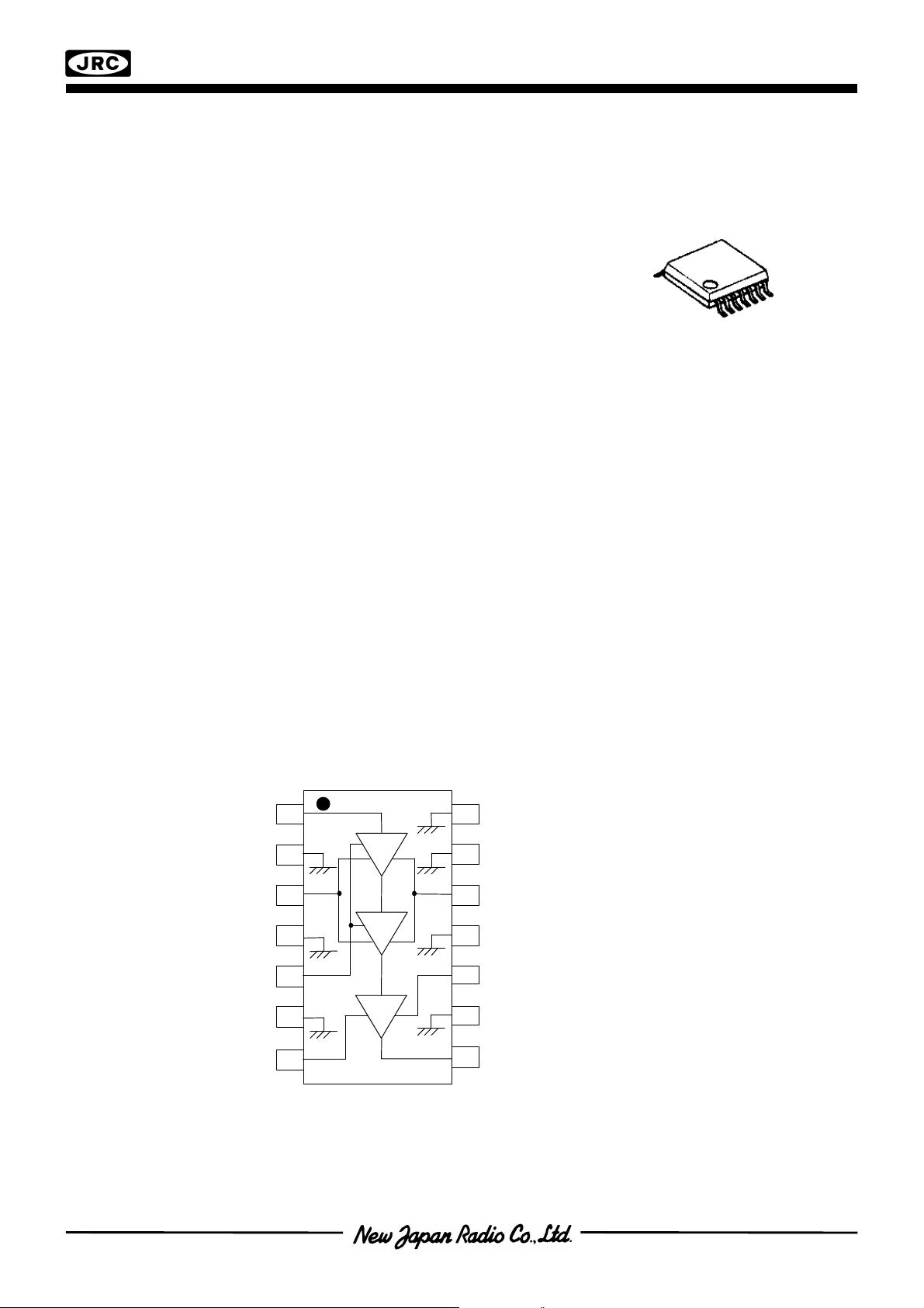
nPIN CONFIGURATION
V Type
(Top View)
1
2
4
5
6
7
14
13
123
11
10
9
8
Pin Connection
1. RF
2. GND
3. V
4. GND
5. V
6. GND
7. V
IN
GG1
CONT
8. RF
9. GND
10. V
11. GND
12. V
13. GND
14. GND
OUT
DD1
DD1
Page 2
NJG1302V
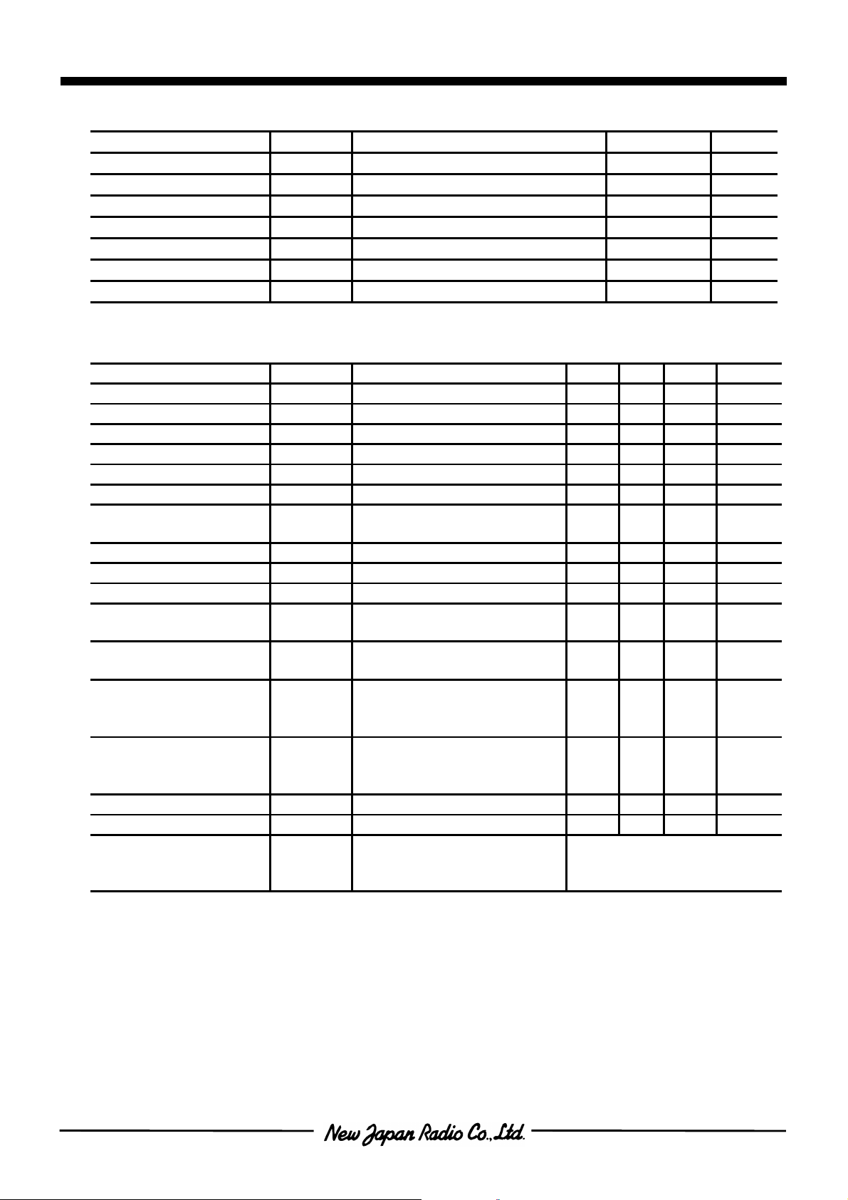
nABSOLUTE MAXIMUM RATINGS
DD1,VDD2
GG1,VGG2
PARAMETER SYMBOL CONDITIONS RATINGS UNITS
Drain Voltage V
Gate Voltage V
Gain Control Voltage V
Input Power P
Power Dissipation P
Operating Temperature T
Storage Temperature T
CONT
in
D
opr
stg
nELECTRICAL CHARACTERISTICS
PARAMETER SYMBOL CONDITONS MIN TYP MAX UNITS
Operating Frequency freq V
Drain Voltage V
Gate Voltage V
Idle Current *1 I
Operating Current *1 I
Gate Current *2 I
Gain Control Terminal
Current
Gain Control Voltage V
DD1,2
GG1,2
idle
DD
GG
I
CONT
CONT
Small Signal Gain Gain V
Gain Flatness G
Gain Control Range G
Pout at 1dB
Compression point
Adjacent Channel
Leakage Power 1
Adjacent Channel
Leakage Power 2
Harmonics P
P
P
P
flat
CONT
-1dB
acp
acp
SP
Input VSWR VSWRiV
Load VSWR Tolerance -
(Ta=+25oC, Zs=Zl=50Ω)
V
GG1,VGG2
V
DD1,VDD2
V
DD1,VDD2
V
DD1,VDD2
=-0.9V 6 V
=-3.0V -4 V
=-3.0V -4 V
=-3.0V, V
GG1,VGG2
=-0.9V 3 dBm
At on PCB board 600 mW
-30 ~ +85 °C
-40 ~ +150 °C
(Ta=+25 oC, Zs=Zl=50Ω)
=3.0V 1.89 - 1.92 GHz
DD1,2
2.9 3.0 5.0 V
V
=3.0V, I
DD1,2
V
=3.0V, No RF Signal 175 180 185 mA
DD1,2
V
=3.0V, P
DD1,2
V
=3.0V, P
DD1,2
V
=3.0V, P
DD1,2
-2.0<V
CONT
=180mA -1.25 -0.9 -0.6 V
idle
=21dBm 180 195 205 mA
out
=21dBm -150 -70 - uA
out
=21dBm
out
<0.0V
-5 -2 - uA
-2.0 - 0 V
DD1,2
V
DD1,2
V
CONT
I
idle
V
DD1,2
V
DD1,2
offset=600kHz,
1
=3.0V, I
=3.0V, I
=-2~0V, V
=180mA
=3.0V 22 23 - dBm
=3.0V, P
=180mA 29 32 35 dB
idle
=180mA 0 0.5 1.0 dB
idle
=3.0V
DD1,2
=21dBm
out
18 20 23 dB
- -60 -55 dBc
Pin;π/4 DQPSK
V
DD1,2
offset=900kHz,
2
=3.0V, P
=21dBm
out
- -65 -60 dBc
Pin; π/4 DQPSK
V
=3.0V, P
DD1,2
=3.0V - - 2.2
DD1,2
V
=3.0V, P
DD1,2
Load VSWR=4:1,All Phase
=21dBm - -35 -30 dBc
out
=21dBm
out
Parasitic Oscillation for
Fundamental Signal Level
:<-60dBc
*1:V
*2:V
Terminal V
DD1
Terminal V
GG1
Terminal Total Current
DD2
Terminal Total Current
GG2
Page 3
NJG1302V
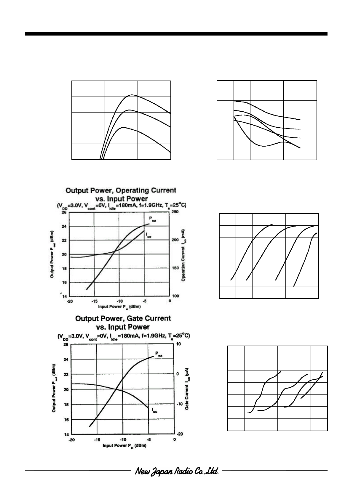
nTYPICAL CHARACTERISTICS
(d
Gain vs. Frequency vs. Control Voltage
(VDD=3.0V, IDD=180mA, Ta=25oC)
40
30
P
vs. Operating Current vs. V
acp
(P
=21dBm, V
out
-50
V
=0V
CONT
-55
=0V, f=1.9GHz, Ta=25oC)
cont
DD
20
Gain (dB)
10
0
-10
0.0 1.0 2.0 3.0
Frequency f (GHz)
-1.0V
-1.4V
Bc)
-60
(dBc)
acp
acp
P
P
-65
-70
150 160 170 180 190 200 210
Operating Current IDD (mA)
VDD=2.9V
4.0V
Output Power vs. Input Power
vs. Control Voltage
(VDD=3.0V, I
26
24
22
(dBm)
out
20
18
16
Output Power P
14
=180mA, f=1.9GHz, Ta=25oC)
idle
V
=0V
CONT
3.0V
3.3V
5.0V
-1V -1.2V
-1.4V
12
-20 -15 -10 -5 0 5 10
P
vs. Input Power vs. Control Voltage
acp
(VDD=3.0V, I
-20
-30
-40
-50
(dBc)
acp
-60
P
-70
-80
-90
-20 -15 -10 -5 0 5 10
Input Power Pin (dBm)
=180mA, f=1.9GHz, Ta=25oC)
idle
V
=0V
CONT
Input Power Pin (dBm)
-1V
-1.2V
-1.4V
Page 4
NJG1302V
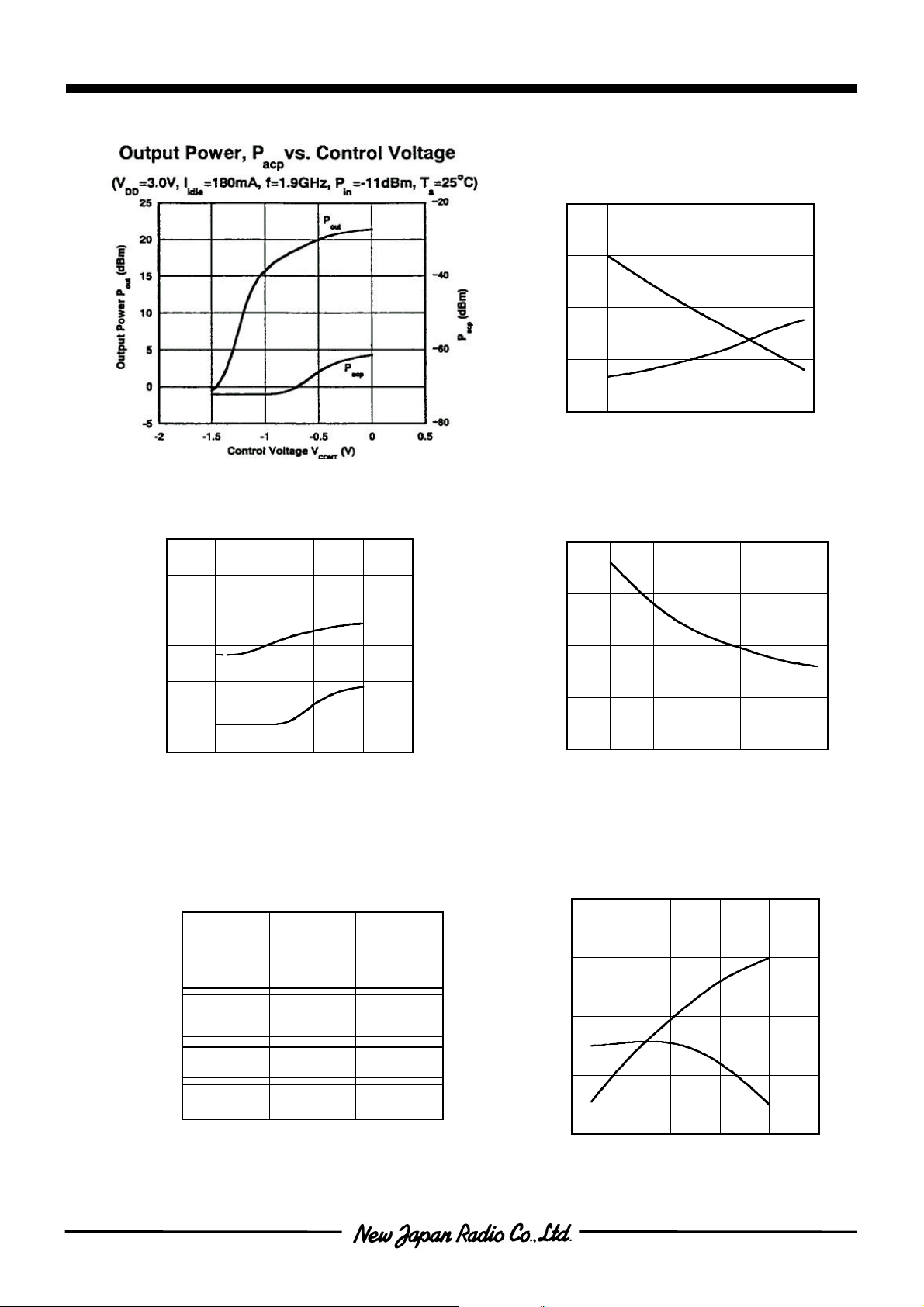
nTYPICAL CHARACTERISTICS
Gain vs PHS Band Frequency
Operating Current, P
(VDD=3.0V, I
250
(mA)
200
DD
150
Operating Current I
=180mA, f=1.9GHz, Pin=-11dBm, Ta=25oC)
idle
vs. Control Voltage
acp
I
DD
P
acp
-20
-40
-60
(dBc)
acp
P
Gain, P
(VDD=3.0V, V
34
33
32
Gain (dB)
31
30
-40 -20 0 20 40 60 80
vs. Ambient Temperature
acp
cont
=0V, I
=180mA, P
idle
Gain
P
acp
Ambient Temperature Ta (oC)
=21dBm, f=1.9GHz)
out
-55
-60
-65
(dBc)
acp
P
Operating Current vs. Ambient Temperature
(VDD=3.0V, V
190
185
(mA)
DD
180
175
Operating Current I
cont
=0V, I
=180mA, P
idle
=21dBm, f=1.9GHz)
out
100
-2 -1.5 -1 -0.5 0 0.5
Control Voltage V
CONT
(V)
vs. Control Voltage
50
40
30
Gain (dB)
20
10
0
1.89 1.9 1.91 1.92
(VDD=3.0V, IDD=180mA, Ta=25oC)
Frequency f (GHz)
V
CONT
=0V
-1.0V
-1.4V
-80
170
-40 -20 0 20 40 60 80
Ambient Temperature Ta (oC)
Gain, Operating Current vs. V
(V
=0V, I
cont
Gain (dB)
=180mA@VDD=3.6V, P
idle
33
32
31
30
29
2.5 3 3.5 4 4.5 5
Drain Voltage VDD (V)
=21dBm, f=1.9GHz, Ta=25oC)
out
I
DD
Gain
DD
240
220
(mA)
DD
200
Operatin Current I
180
160
Page 5
NJG1302V
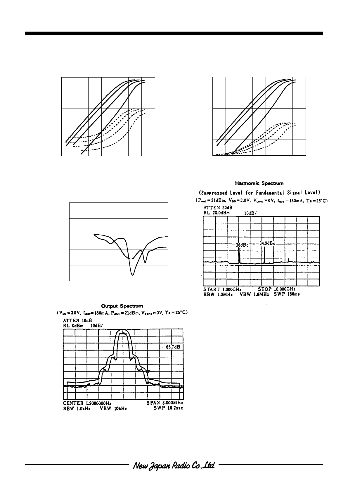
nTYPICAL CHARACTERISTICS
Output Power,Total Current vs. Input Power
( V
=3V, V
DD2,3
25
20
(dBm)
15
out
10
Output Power P
5
0
-25 -20 -15 -10 -5 0 5 10
=0V, f=1.9GHz, Ta=25oC)
CONT
Output Power
@I
=80mA
idle
60mA
40mA
20mA
Input Power Pin (dBm)
60mA
40mA
20mA
Total Current
@I
=80mA
idle
350
300
250
200
150
Total Current (mA)
100
50
0
|S11| , |S22| vs. Frequency
(VDD=3.0V, IDD=180mA, V
20
10
=0V, Ta=25oC)
cont
Output Power, P.A.E. vs. Input Power
( V
=3V, V
DD2,3
25
20
(dBm)
15
out
10
Output Power P
5
0
-25 -20 -15 -10 -5 0 5 10
=0V, f=1.9GHz, Ta=25oC )
CONT
Output Power
@I
=80mA
idle
Input Power Pin (dBm)
60mA
40mA
@I
idle
60mA
40mA
20mA
P.A.E.
=80mA
20mA
100
80
60
40
20
0
Power Added Efficiency (%)
| (dB)
22
| , |S
11
|S
0
-10
-20
-30
0 1 2 3
Frequency f (GHz)
|S22|
|S11|
W
All adjacent channel leakage power used in these evaluations are those of 600kHz offset from
fundamental wave at PHS operating condition(π/4QPSK moduration)
Page 6
NJG1302V
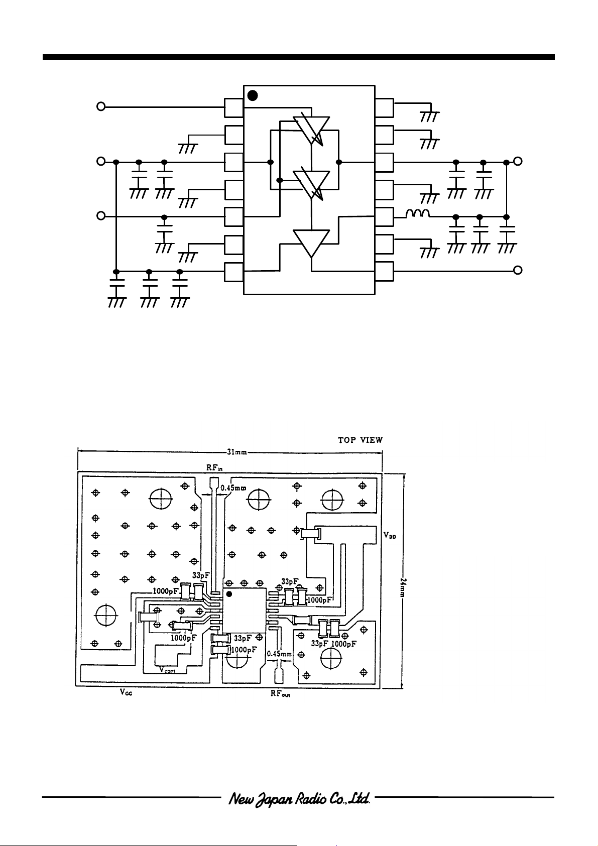
nRECOMMENDED CIRCUIT
1uF
PCB : FR4 t=0.2mm
4.7uF
RFin
GG
V
(-0.5~-1.2V)
IDD=0 @VGG <-2V
V
(0~-2V)
=
cont
C
C
1
C
3
2
C
2
C
1
C
1
nRECOMMENDED PCB DESIGN
GND
GND
VDD1
GND
VDD2
GND
RFout
14
13
12
11
10
DD
V
C
2
L
1
C
2
9
87
(3.0~5.0V)
C
1
C
C
3
1
RFout
1
RFin
GND2
3
VGG1
4
GND
5
cont
V
6
GND
VGG2
C1: 1000pF
C2: 33pF
C3: 1uF
L1: 4.7nH
The reflow method is recommended for this device to attach on PCB
1uF
CAPACITOR
MURATA GRM39 Series
INDUCTOR
TAIYO-YUDEN HK1608 Series
Page 7
NJG1302V
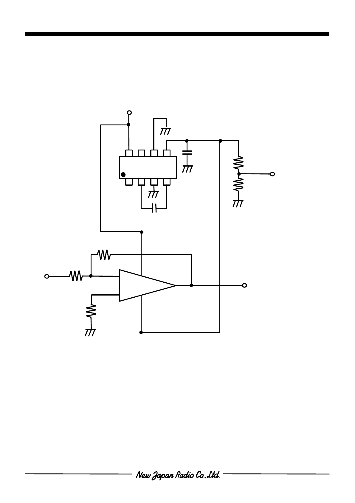
nAPPLICATION CIRCUIT (NEGATIVE VOLTAGE GENERATOR)
-3.0V
+3.0V
500kΩ
1MΩ1MΩ(3kΩ)
(7kΩ)
NJU7001
NJU7660
-
8 7 6 5
1 2 3 4
+ -
10uF
+
10kΩTrimmer Resistance
VGG
(-0.9V Typ.)
V
CONT
(0~+2V)
10uF
+V
2
3
7
6
out
4
-V
V
cont
(0~-2V)
Page 8
NJG1302V
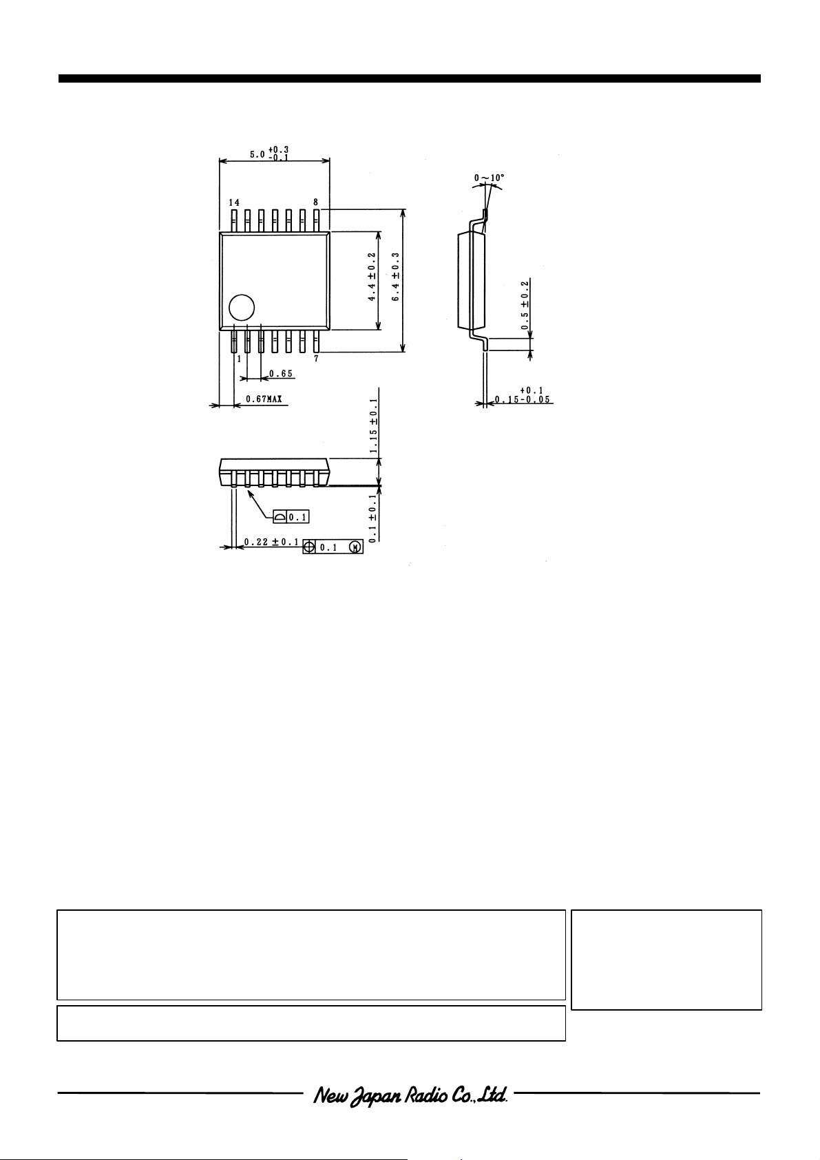
nPACKAGE OUTLINE (SSOP14)
• To waste this product, please obey the relating law of your country.
with care to avoid these damages .
[CAUTION]
Lead material : Copper
Lead surface finish : Solder plating
Molding material : Epoxy resin
UNIT : mm
Weight :66mg
Cautions on using this product
This product contains Gallium-Arsenide (GaAs) which is a harmful material.
• Do NOT eat or put into mouth.
• Do NOT dispose in fire or break up this product.
• Do NOT chemically make gas or powder with this product.
This product may be damaged with electric static discharge (ESD) or spike voltage. Please handle
The specifications on this databook are only
given for information , without any guarantee
as regards either mistakes or omissions. The
application circuits in this databook are
described only to show representative usages
of the product and not intended for the
guarantee or permission of any right including
the industrial rights.
 Loading...