

NJG1708PC1
Ver 0.3 11/02 ’99
TENTATIVE
800MHz BAND DOWNCONVERTER GaAs MMIC
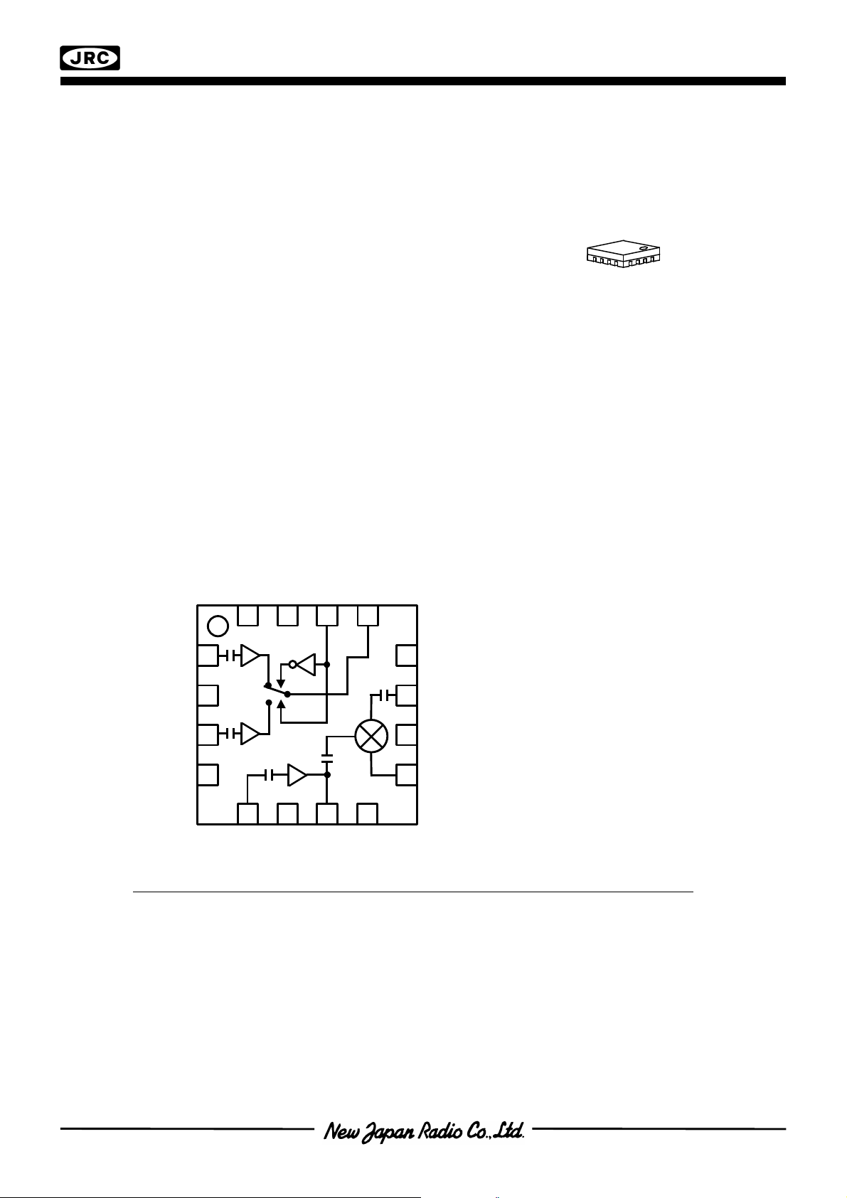
nGENERAL DESCRIPTION nPACKAGE OUTLINE
NJG1708PC1 is a downconverter GaAs MMIC including
a 2xLNA, local amplifier and MIXER, designed NJG1708PC1
exhibits mainly for 800MHz band cellular phone.
The Ultra Small & Thin FFP16-C1 package is applied.
NJG1708PC1
nFEATURES
lLow voltage operation +3.0V typ.
lLow current consumption 9mA typ.
lHigh conversion gain 28dB typ. @fRF=820MHz, PRF=-50dBm, fLO=690MHz, PLO=-15dBm
lLow noise figure 1.7dB typ. @fRF=820MHz, fLO=690MHz, PLO=-15dBm
lHigh Input IP3 -14dBm typ. @fRF=820.0+820.1MHz, fLO=690MHz, PLO=-15dBm
lUltra Small & Thin Package FFP16-C1 (Mount Size: 2.5mmX2.5mmX0.85mm)
nBLOCK DIAGRAM
PC1 Type
(Top View)
16
15 14 13
1
2
3
4
5 6
NOTE: Please note that any information on this catalog will be subject to change.
7
12
11
10
9
8
Pin Connection
1.LNAIN1
2.GND
3. LNAIN2
4.GND
5.LOIN
6.GND
7.V
LO
8.GND
9.IFOUT
10.GND
11.MIXIN
12.GND
13.LNAOUT
14.V
CTL
15.GND
16.V
INV
- 1 -
NJG1708PC1
nABSOLLUTE MAXIMUM RATINGS
o
(Ta=+25°C, Zs=Zl=50Ω)
PARAMETER SYMBOL CONDITIONS RATINGS UNITS
LNA Voltage V
Mixer Voltage V
Local Amplifier Voltage V
Input Power 1 P
Input Power 2 P
Power Dissipation P
Operating Temperature T
Storage Temperature T
LNA
MIX
LO
LNAIN
LOIN
D
opr
stg
V
LNA=VMIX=VLO
V
LNA=VMIX=VLO
=2.7V +15 dBm
=2.7V +10 dBm
5.0 V
5.0 V
5.0 V
320 mW
-40~+85 °C
-55~+125 °C
nELECTRICAL CHARACTERISTICS (LNA)
COMMON CONDITIONS: Ta=-20~+75°C, V
=3.0V, V
LNA
=3.0V, V
INV
MIX=VLO
=0V, fRF=820MHz,
Zs=Zl=50Ω, Measuring Test Circuit (fLO=690MHz)
PARAMETERS SYMBOL CONDITIONS MIN TYP MAX UNITS
Operating Frequency freq 800 820 900 MHz
LNA Voltage V
LNA Current I
LNA Operating Voltage (LOW) V
LNA Operating Voltage (HIGH) V
LNA
LNA
CTL(L)
CTL(H)
PRF, PLO=OFF - 3.0 4.0 mA
2.5 3.0 4.5 V
- 0 0.8 V
2.4 3.0 - V
Small Signal Gain Gain 14.0 15.5 18.0 dB
Noise Figure NF - 1.4 - dB
fRF=810±10MHz
Gain Flatness G
flat
fRF=893.5±4.5MHz
- - 0.5 dB
fRF=877.5±7.5MHz
Output 3rd order
Intercept point
OIP3 fRF=820.0+820.1MHz - 13.0 - dBm
Isolation ISO - 30.0 - dB
RF IN VSWR VSWR
RF OUT VSWR VSWR
i
- 1.5 2.0 -
- 2.0 - -
nELECTRICAL CHARACTERISTICS (MIXER)
COMMON CONDITIONS: Ta=-20~+75°C, V
LNA
=0V, V
MIX=VLO
=3.0V, V
=0V, fRF=820MHz,
INV
fLO=690MHz, PRF=-30dBm, PLO=-15dBm, Zs=Zl=50Ω,
Measuring Test Circuit (fLO=690MHz)
PARAMETERS SYMBOL CONDITIONS MIN TYP MAX UNITS
Operating Frequency freq 800 820 900 MHz
Mixer Voltage V
Mixer Current I
Local Amplifier Current I
Conversion Gain G
MIX
MIX
LO
PRF, PLO=OFF - 5.0 6.7 mA
PRF, PLO=OFF - 1.0 2.0 mA
c
2.5 3.0 4.5 V
- 12.0 - dB
Noise Figure NF - 5.0 6.0 dB
Output 3rd order
Intercept point
OIP3 fRF=820.0+820.1MHz - +14.5 - dBm
Local Leak Pleak PLO=-10dBm - -26.0 -20.0 dBm
- 2 -

NJG1708PC1
nRECOMMENDED CIRCUIT
LOCAL IN
Ω
Ω
Ω
Ω
Ω
V
=3V
INV
L2
RF IN 1
Zo=50
L1
L4
RF IN 2
Zo=50
L3
Zo=50
C11
1
2
3
4
C2
V
=0/3V
CTL
16
LNA1
LNA2
LOCAL AMP
L9
15
C12
MIXER
R1
L6
C5
V
=3V
LNA
C1
L5
1314
12
RF OUT
Zo=50
L7
11
MIXER IN
L8
10
L11
9
C3
L12
C4
IF OUT
Zo=50
8765
C8 C9
V
=3V
MIX
C10
L10
C6
C7
VLO=3V
- 3 -

NJG1708PC1
nPACKAGE OUTLINE (FFP16)
UNITS : mm
±
(TOP VIEW)
1pin INDEX
0.30
0.10
0.30
0.85±0.15
2pin INDEX
0.1
0.17
0.50
0.50
0.365
Cautions on using this product
This product contains Gallium-Arsenide (GaAs) which is a harmful material.
• Do NOT eat or put into mouth.
• Do NOT dispose in fire or break up this product.
• Do NOT chemically make gas or powder with this product.
• To waste this product, please obey the relating law of your country.
This product may be damaged with electric static discharge (ESD) or spike voltage. Please handle
with care to avoid these damages.
• The product specifications and descriptions listed in this catalog are subject to change
without prior notice.
• New Japan Radio have no responsibilities on any violation of the right of the patent
by the third party who contains the information and drawing in this catalog.
• This product is not designed for the system requiring high reliability, such as space or
air system, submarine cable system, nuclear power plant control system or medical
instrument for life keeping.
If you are planning to use in the system above, please ask for our sales representatives.
• The technology or freights of this device may be controlled by the regulation on the Foreign
Export and the Foreign Export Control Law.
(BOTTOM VIEW)
0.50
0.50
2.50±0.1
0.20
0.27
0.5 0.5
2.50
PCB : Ceramic
OVER COART : Epoxy resin
LEAD SURFACE : Au
- 4 -

MEMO
[CAUTION]
The specif ications on this da tabook are only
given f or information , without any g uarantee
as regards e ither mistakes or omi ssions. The
applicatio n circuits in this d atabook are
described only to show representative us ages
of the prod uct and not intended for th e
guarantee or per mission of any rig ht including
the industri al rights.
 Loading...