

Page 1
NJG1524PC1
- 1 -
DPDT SWITCH GaAs MMIC
n
GENERAL DESCRIPTION
n
PACKAGE OUTLINE
NJG1524PC1 is a DPDT switch GaAs MMIC.
The two same switches are merged into one package
and functionally linked. It is useful for switching two
circuits in-line.
Each switches feature very low loss, high isolation and
wide frequency coverage from 50MHz to 3GHz at low
control voltage of 2.5V.
The ultra small & thin FFP16-C1package is adopted.
n
FEATURES
lSingle low voltage control +2.5~+6.5V
lLow insertion loss 0.3dB typ.@f=1GHz, Pin=0dBm, each switch
0.5dB typ.@f=2GHz, Pin=0dBm, each switch
lHigh isolation 42dB typ. @f=2GHz,PC1-PC2
27dB typ.@f=2GHz, PC1-PA1 PC1-PA2, PC2-PB1,
PC2-PB2, PA1-PA2, PB1-PB2
lHanding power 20dBm max. @f=2GHz, V
CTL
=2.7V
lLow current consumption 16uA typ.@f=2GHz, Pin=10dBm
lUltra small & thin package FFP16-C1 (Mount Size: 2.5x2.5x0.85mm)
n
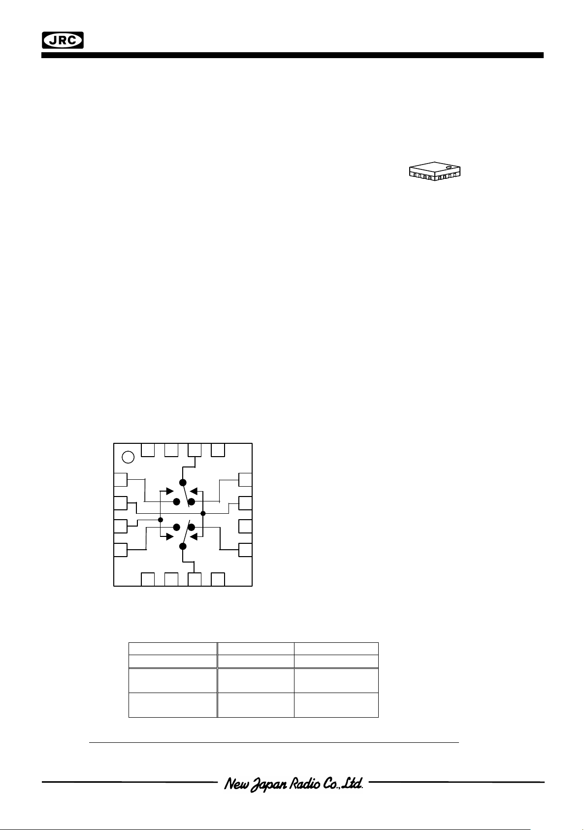
PIN CONFIGURATION
n
TRUTH TABLE
V
CTL1
H L
V
CTL2
L H
PC1 – PA1
PC2 – PB1
ON OFF
PC1 – PA2
PC2 – PB2
OFF ON
FFP16 Type
(Top View)
TENTATIVE Ver.1
04/04/2000
NJG1524PC1
“H”=V
CTL(H)
, “L”=V
CTL(L)
Pin Connection
1.PA2 9.PB1
2.V
CTL1
10.NC
3.V
CTL2
11.V
CTL1
4.PB2 12.PA1
5.GND 13.GND
6.GND 14.PC1
7.PC2 15.GND
8.GND 16.GND
NOTE: Please note that any information on this catalog will be subject to change.
4
2
5
3
6
1
7
8
9
10
11
12
13
14
1516
Page 2
NJG1524PC1
- 2 -
n
ABSOLUTE MAXIMUM RATINGS
(Ta=25°C)
PARAMETER SYMBOL CONDITIONS RATINGS UNITS
Input Power P
in
V
CTL(L)
=0V, V
CTL(H)
=2.7V 28 dBm
Control voltage V
CTL
V
CTL(H)
- V
CTL(L)
7.5 V
Power Dissipation P
D
400 mW
Operating Temp. T
opr
-40~+85 °C
Storage Temp. T
stg
-55~+125 °C
n
ELECTRACAL CHARACTERISTICS (EACH SWITCH)
(V
CTL (L)
=0V, V
CTL (H)
=2.7V, ZS=ZO=50Ω, Ta=25°C)
PARAMETER SYMBOL CONDITIONS MIN TYP MAX UNITS
Operating voltage (L) V
CTL(L)
-0.2 0 0.2 V
Operating voltage (H) V
CTL(H)
2.5 2.7 6.5 V
Control Current I
CTL
f=2GHz, Pin=10dBm - 16 28 uA
Insertion loss1 Loss1
PC1-PA1, PC1-PA2,
PC2-PB1, PC2-PB2 ON,
f=1GHz, Pin=0dBm
- 0.3 0.6 dB
Insertion loss2 Loss2
PC1-PA1, PC1-PA2,
PC2-PB1, PC2-PB2 ON,
f=2GHz, Pin=0dBm
- 0.5 0.8 dB
Isolation1 ISL1
PC1-PA1, PC1-PA2,
PC2-PB1, PC2-PB2 OFF,
f=1GHz, Pin=0dBm
25.5 27 - dB
Isolation2 ISL2
PC1-PA1, PC1-PA2,
PC2-PB1, PC2-PB2 OFF,
f=2GHz, Pin=0dBm
25 27 - dB
Isolation3 ISL3
PA1, PA2, PB1, PB2 Port
50Ω terminal, PC1-PC2
port, f=2GHz, Pin=0dBm
39 42 - dB
Pin at 1dB
compression point
P
-1dB
f=2GHz 20 24 - dBm
VSWR (PC, P1, P2) VSWR f=0.05~2GHz, ON State - 1.3 1.6
Switch time T
SW
f=0.05~2.5GHz - 20 60 ns
Page 3

NJG1524PC1
- 3 -
n
TERMINAL INFORMATION
No. SYMBOL DESCRIPTIONS
1 PA2
RF port A2. This port is connected with PC1 port by controlling
VCTL (L)
to
-0.2~+0.2V and
VCTL(H)
to 2.5~6.5V. In order to block the DC bias voltage
of internal circuit, an external capacitor is required.
2 V
CTL1
Control port 1. The voltage of this port controls PC1 to PA1/PA2 and
PC2 to PB1/PB2 state. The ‘ON’ and ‘OFF’ state is toggled by controlling
voltage of this terminal to high-state (2.5~6.5V) or low-state (-
0.2~+0.2V). The voltage of V
CTL2
should be set to opposite state. The
bypass capacitor should be connected with GND as close as possible
for excellent RF performance.
3 V
CTL2
Control port 2. The voltage of this port controls PC1 to PA1/PA2 and
PC2 to PB1/PB2 state. The ‘ON’ and ‘OFF’ state is toggled by controlling
voltage of this terminal to high-state (2.5~6.5V) or low-state (-
0.2~+0.2V). The voltage of V
CTL1
should be set to opposite state. The
bypass capacitor should be connected with GND as close as possible
for excellent RF performance.
4 PB2
RF port B2. This port is connected with PC2 port by controlling V
CTL1
to
–0.2~+0.2V and V
CTL2
to 2.5~6.5V. In order to block the DC bias voltage
of internal circuit, an external capacitor is required.
7 PC2
Common RF port C2. In order to block the DC bias voltage of internal
circuit, an external capacitor is required.
9 PB1
RF port B1. This port is connected with PC1 port by controlling V
CTL2
to
–0.2~+0.2V and V
CTL1
to 2.5~6.5V. In order to block the DC bias voltage
of internal circuit, an external capacitor is required.
10 NC No connected terminal.
11 V
CTL1
Control port 1. The voltage of this port controls PC1 to PA1/PA2 and
PC2 to PB1/PB2 state. The ‘ON’ and ‘OFF’ state is toggled by controlling
voltage of this terminal to high-state (2.5~6.5V) or low-state (-
0.2~+0.2V). The voltage of V
CTL2
should be set to opposite state. The
bypass capacitor should be connected with GND as close as possible
for excellent RF performance.
12 PA1
RF port A1. This port is connected with PC1 port by controlling V
CTL2
to
–0.2~+0.2V and V
CTL1
to 2.5~6.5V. In order to block the DC bias voltage
of internal circuit, an external capacitor is required.
14 PC1
Common RF port C1. In order to block the DC bias voltage of internal
circuit, an external capacitor is required.
5, 6, 8, 13,
15, 16
GND
Ground terminal. Please connect this terminal with ground plane as
close as possible for excellent RF performance.
Page 4
NJG1524PC1
- 4 -
n
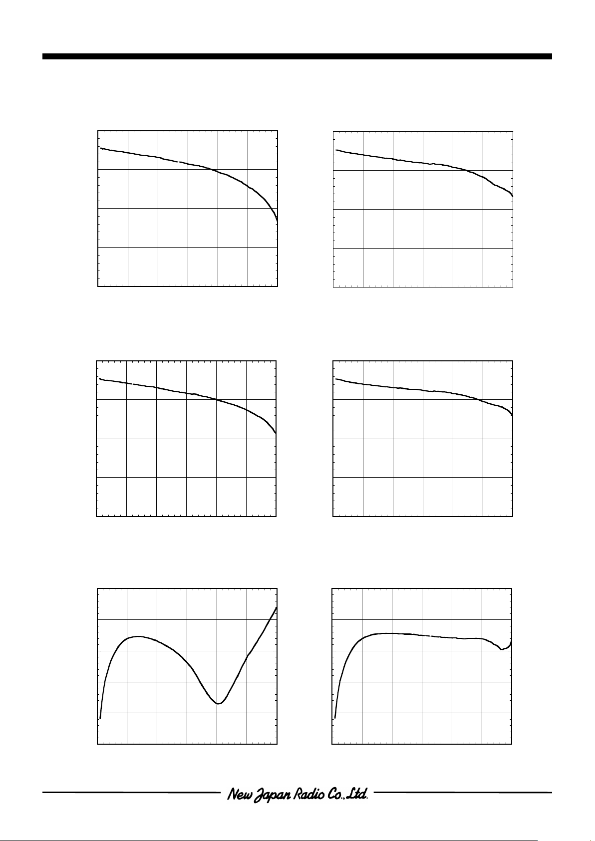
TYPICAL CHARACTERISTICS (50MHz~3GHz, with application circuit, without DC blocking capacitor, losses of circuit are excluded.)
-2.0
-1.5
-1.0
-0.5
0.0
0.0 0.5 1.0 1.5 2.0 2.5 3.0
PC1-PA1 Insertion Loss vs. Frequency
Insertion Loss (dB)
Frequency (GHz)
( VCTL1=2.7V,VCTL2=0V ,Pin=0dBm )
-2.0
-1.5
-1.0
-0.5
0.0
0.0 0.5 1.0 1.5 2.0 2.5 3.0
PC1-PA2 Insertion Loss vs. Frequency
Insertion Loss (dB)
Frequency (GHz)
( VCTL1=0V,VCTL2=2.7V ,Pin=0dBm )
-45
-40
-35
-30
-25
-20
0.0 0.5 1.0 1.5 2.0 2.5 3.0
PC1-PA1 Isolation vs. Frequency
Isolation (dB)
Frequency (GHz)
( VCTL1=0V,VCTL2=2.7V ,Pin=0dBm )
-45
-40
-35
-30
-25
-20
0.0 0.5 1.0 1.5 2.0 2.5 3.0
PC1-PA2 Isolation vs. Frequency
Isolation (dB)
Frequency (GHz)
( VCTL1=2.7V,VCTL2=0V ,Pin=0dBm )
-2.0
-1.5
-1.0
-0.5
0.0
0.0 0.5 1.0 1.5 2.0 2.5 3.0
PC2-PB1 Insertion Loss vs. Frequency
Insertion Loss (dB)
Frequency (GHz)
( VCTL1=2.7V,VCTL2=0V ,Pin=0dBm )
-2.0
-1.5
-1.0
-0.5
0.0
0.0 0.5 1.0 1.5 2.0 2.5 3.0
PC2-PB2 Insertion Loss vs. Frequency
Insertion Loss (dB)
Frequency (GHz)
( VCTL1=0V,VCTL2=2.7V ,Pin=0dBm )
Page 5
NJG1524PC1
- 5 -
n
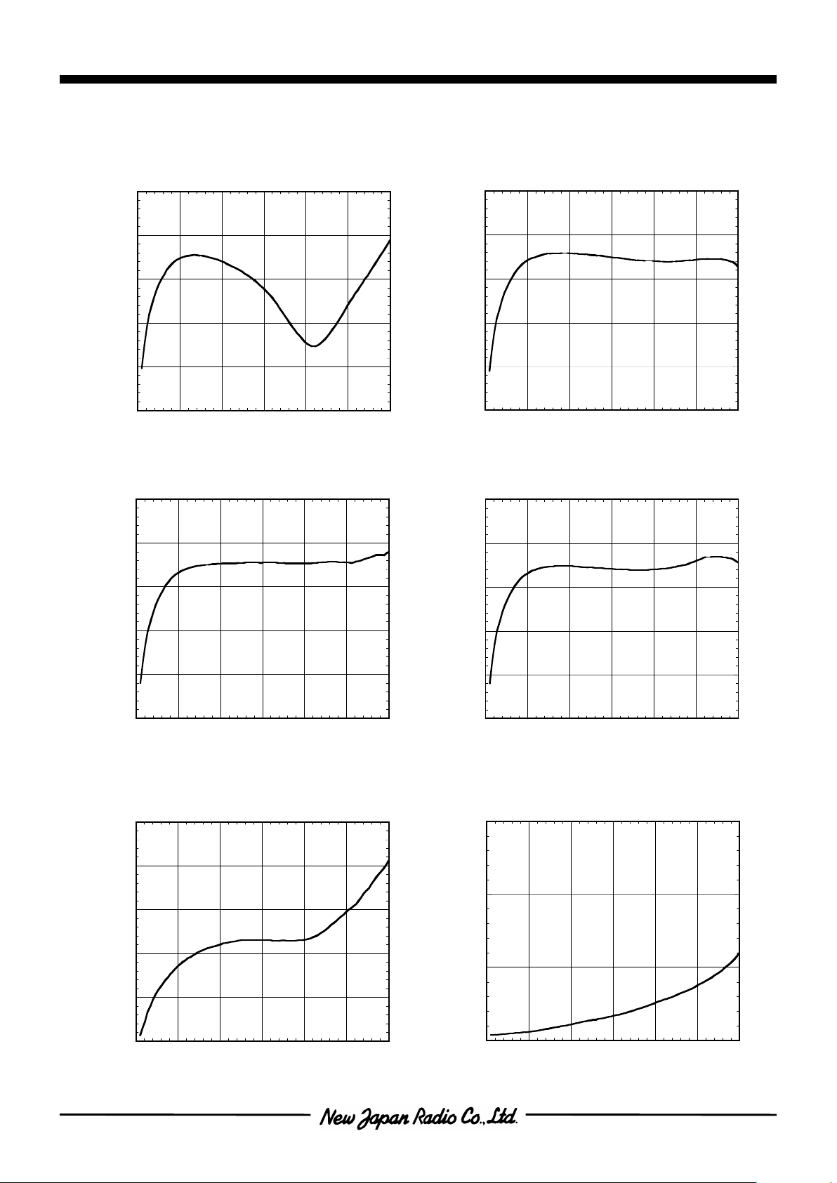
TYPICAL CHARACTERISTICS (50MHz~3GHz, with application circuit, without DC blocking capacitor, losses of circuit are excluded.)
-45
-40
-35
-30
-25
-20
0.0 0.5 1.0 1.5 2.0 2.5 3.0
PC2-PB2 Isolation vs. Frequency
Isolation (dB)
Frequency (GHz)
( VCTL1=2.7V,VCTL2=0V ,Pin=0dBm )
-45
-40
-35
-30
-25
-20
0.0 0.5 1.0 1.5 2.0 2.5 3.0
PB1-PB2 Isolation vs. Frequency
Isolation (dB)
Frequency (GHz)
( VCTL1=2.7V,VCTL2=0V ,Pin=0dBm )
-45
-40
-35
-30
-25
-20
0.0 0.5 1.0 1.5 2.0 2.5 3.0
PC2-PB1 Isolation vs. Frequency
Isolation (dB)
Frequency (GHz)
( VCTL1=0V,VCTL2=2.7V ,Pin=0dBm )
-45
-40
-35
-30
-25
-20
0.0 0.5 1.0 1.5 2.0 2.5 3.0
PA1-PA2 Isolation vs. Frequency
Isolation (dB)
Frequency (GHz)
( VCTL1=2.7V,VCTL2=0V ,Pin=0dBm )
-70
-60
-50
-40
-30
-20
0.0 0.5 1.0 1.5 2.0 2.5 3.0
PC1-PC2 Isolation vs. Frequency
Isolation (dB)
Frequency (GHz)
( VCTL1=2.7V,VCTL2=0V ,Pin=0dBm )
1.0
1.5
2.0
2.5
0.0 0.5 1.0 1.5 2.0 2.5 3.0
PC1-PA1(on) VSWR vs. Frequency
VSWR
Frequency (GHz)
( VCTL1=2.7V,VCTL2=0V,PC1 port )
Page 6
NJG1524PC1
- 6 -
n
TYPICAL CHARACTERISTICS (50MHz~3GHz, with application circuit, without DC blocking capacitor, losses of circuit are excluded.)
1.0
1.5
2.0
2.5
0.0 0.5 1.0 1.5 2.0 2.5 3.0
PC1-PA2(on) VSWR vs. Frequency
VSWR
Frequency (GHz)
( VCTL1=0V,VCTL2=2.7V,PC1 port )
1.0
1.5
2.0
2.5
0.0 0.5 1.0 1.5 2.0 2.5 3.0
PC2-PB1(on) VSWR vs. Frequency
VSWR
Frequency (GHz)
( VCTL1=2.7V,VCTL2=0V,PC2 port )
1.0
1.5
2.0
2.5
0.0 0.5 1.0 1.5 2.0 2.5 3.0
PC2-PB2(on) VSWR vs. Frequency
VSWR
Frequency (GHz)
( VCTL1=0V,VCTL2=2.7V,PC2 port )
Page 7

NJG1524PC1
- 7 -
n
TYPICAL CHARACTERISTICS (50MHz~100MHz, with application circuit, losses of PCB,
connector and DC blocking capacitor (0.01uF) are included.)
-2.0
-1.5
-1.0
-0.5
0.0
50 60 70 80 90 100
PC1-PA1 Insertion Loss vs. Frequency
Insertion Loss (dB)
Frequency (MHz)
( VCTL1=2.7V,VCTL2=0V ,Pin=0dBm )
-2.0
-1.5
-1.0
-0.5
0.0
50 60 70 80 90 100
PC1-PA2 Insertion Loss vs. Frequency
Insertion Loss (dB)
Frequency (MHz)
( VCTL1=0V,VCTL2=2.7V ,Pin=0dBm )
-2.0
-1.5
-1.0
-0.5
0.0
50 60 70 80 90 100
PC2-PB1 Insertion Loss vs. Frequency
Insertion Loss (dB)
Frequency (MHz)
( VCTL1=2.7V,VCTL2=0V ,Pin=0dBm )
-2.0
-1.5
-1.0
-0.5
0.0
50 60 70 80 90 100
PC2-PB2 Insertion Loss vs. Frequency
Insertion Loss (dB)
Frequency (MHz)
( VCTL1=0V,VCTL2=2.7V ,Pin=0dBm )
-50
-40
-30
-20
50 60 70 80 90 100
PC1-PA1 Isolation vs. Frequency
Isolation (dB)
Frequency (MHz)
( VCTL1=0V,VCTL2=2.7V ,Pin=0dBm )
-50
-40
-30
-20
50 60 70 80 90 100
PC1-PA2 Isolation vs. Frequency
Isolation (dB)
Frequency (MHz)
( VCTL1=2.7V,VCTL2=0V ,Pin=0dBm )
Page 8

NJG1524PC1
- 8 -
n
TYPICAL CHARACTERISTICS (50MHz~100MHz, with application circuit, losses of PCB,
connector and DC blocking capacitor (0.01uF) are included.)
-50
-40
-30
-20
50 60 70 80 90 100
PC2-PB1 Isolation vs. Frequency
Isolation (dB)
Frequency (MHz)
( VCTL1=0V,VCTL2=2.7V ,Pin=0dBm )
-50
-40
-30
-20
50 60 70 80 90 100
PC2-PB2 Isolation vs. Frequency
Isolation (dB)
Frequency (MHz)
( VCTL1=2.7V,VCTL2=0V ,Pin=0dBm )
-50
-40
-30
-20
50 60 70 80 90 100
PA1-PA2 Isolation vs. Frequency
Isolation (dB)
Frequency (MHz)
( VCTL1=2.7V,VCTL2=0V ,Pin=0dBm )
-50
-40
-30
-20
50 60 70 80 90 100
PB1-PB2 Isolation vs. Frequency
Isolation (dB)
Frequency (MHz)
( VCTL1=2.7V,VCTL2=0V ,Pin=0dBm )
-80
-70
-60
-50
-40
-30
50 60 70 80 90 100
PC1-PC2 Isolation vs. Frequency
Isolation (dB)
Frequency (MHz)
( VCTL1=2.7V,VCTL2=0V ,Pin=0dBm )
Page 9

NJG1524PC1
- 9 -
n
TYPICAL CHARACTERISTICS (0.1GHz~0.5GHz, with application circuit, losses of PCB, connector
and DC blocking capacitor (1000pF) are included.)
-2.0
-1.5
-1.0
-0.5
0.0
100 200 300 400 500
PC1-PA1 Insertion Loss vs. Frequency
Insertion Loss (dB)
Frequency (MHz)
( VCTL1=2.7V,VCTL2=0V ,Pin=0dBm )
-2.0
-1.5
-1.0
-0.5
0.0
100 200 300 400 500
PC1-PA2 Insertion Loss vs. Frequency
Insertion Loss (dB)
Frequency (MHz)
( VCTL1=0V,VCTL2=2.7V ,Pin=0dBm )
-2.0
-1.5
-1.0
-0.5
0.0
100 200 300 400 500
PC2-PB1 Insertion Loss vs. Frequency
Insertion Loss (dB)
Frequency (MHz)
( VCTL1=2.7V,VCTL2=0V ,Pin=0dBm )
-2.0
-1.5
-1.0
-0.5
0.0
100 200 300 400 500
PC2-PB2 Insertion Loss vs. Frequency
Insertion Loss (dB)
Frequency (MHz)
( VCTL1=0V,VCTL2=2.7V ,Pin=0dBm )
-50
-40
-30
-20
100 200 300 400 500
PC1-PA1 Isolation vs. Frequency
Isolation (dB)
Frequency (MHz)
( VCTL1=0V,VCTL2=2.7V ,Pin=0dBm )
-50
-40
-30
-20
100 200 300 400 500
PC1-PA2 Isolation vs. Frequency
Isolation (dB)
Frequency (MHz)
( VCTL1=2.7V,VCTL2=0V ,Pin=0dBm )
Page 10

NJG1524PC1
- 10 -
n
TYPICAL CHARACTERISTICS (0.1GHz~0.5GHz, with application circuit, losses of PCB, connector
and DC blocking (1000pF) are included.)
-50
-40
-30
-20
100 200 300 400 500
PC2-PB1 Isolation vs. Frequency
Isolation (dB)
Frequency (MHz)
( VCTL1=0V,VCTL2=2.7V ,Pin=0dBm )
-50
-40
-30
-20
100 200 300 400 500
PC2-PB2 Isolation vs. Frequency
Isolation (dB)
Frequency (MHz)
( VCTL1=2.7V,VCTL2=0V ,Pin=0dBm )
-50
-40
-30
-20
100 200 300 400 500
PA1-PA2 Isolation vs. Frequency
Isolation (dB)
Frequency (MHz)
( VCTL1=2.7V,VCTL2=0V ,Pin=0dBm )
-50
-40
-30
-20
100 200 300 400 500
PB1-PB2 Isolation vs. Frequency
Isolation (dB)
Frequency (MHz)
( VCTL1=2.7V,VCTL2=0V ,Pin=0dBm )
-80
-70
-60
-50
-40
-30
100 200 300 400 500
PC1-PC2 Isolation vs. Frequency
Isolation (dB)
Frequency (MHz)
( VCTL1=2.7V,VCTL2=0V ,Pin=0dBm )
Page 11

NJG1524PC1
- 11 -
n
TYPICAL CHARACTERISTICS (0.5GHz~3GHz, with application circuit, losses of PCB, connector
and blocking capacitor (56pF) are included.)
-2.0
-1.5
-1.0
-0.5
0.0
0.5 1.0 1.5 2.0 2.5 3.0
PC1-PA1 Insertion Loss vs. Frequency
Insertion Loss (dB)
Frequency (GHz)
( VCTL1=2.7V,VCTL2=0V ,Pin=0dBm )
-2.0
-1.5
-1.0
-0.5
0.0
0.5 1.0 1.5 2.0 2.5 3.0
PC1-PA2 Insertion Loss vs. Frequency
Insertion Loss (dB)
Frequency (GHz)
( VCTL1=0V,VCTL2=2.7V ,Pin=0dBm )
-2.0
-1.5
-1.0
-0.5
0.0
0.5 1.0 1.5 2.0 2.5 3.0
PC2-PB1 Insertion Loss vs. Frequency
Insertion Loss (dB)
Frequency (GHz)
( VCTL1=2.7V,VCTL2=0V ,Pin=0dBm )
-2.0
-1.5
-1.0
-0.5
0.0
0.5 1.0 1.5 2.0 2.5 3.0
PC2-PB2 Insertion Loss vs. Frequency
Insertion Loss (dB)
Frequency (GHz)
( VCTL1=0V,VCTL2=2.7V ,Pin=0dBm )
-50
-40
-30
-20
0.5 1.0 1.5 2.0 2.5 3.0
PC1-PA1 Isolation vs. Frequency
Isolation (dB)
Frequency (GHz)
( VCTL1=0V,VCTL2=2.7V ,Pin=0dBm )
-50
-40
-30
-20
0.5 1.0 1.5 2.0 2.5 3.0
PC1-PA2 Isolation vs. Frequency
Isolation (dB)
Frequency (GHz)
( VCTL1=2.7V,VCTL2=0V ,Pin=0dBm )
Page 12

NJG1524PC1
- 12 -
n
TYPICAL CHARACTERISTICS (0.5GHz~3GHz, with application circuit, losses of PCB, connector
and DC blocking capacitor (56pF) are included.)
-40
-30
-20
-10
0.5 1.0 1.5 2.0 2.5 3.0
PA1-PA2 Isolation vs. Frequency
Isolation (dB)
Frequency (GHz)
( VCTL1=2.7V,VCTL2=0V ,Pin=0dBm )
-40
-30
-20
-10
0.5 1.0 1.5 2.0 2.5 3.0
PB1-PB2 Isolation vs. Frequency
Isolation (dB)
Frequency (GHz)
( VCTL1=2.7V,VCTL2=0V ,Pin=0dBm )
-50
-40
-30
-20
0.5 1.0 1.5 2.0 2.5 3.0
PC2-PB1 Isolation vs. Frequency
Isolation (dB)
Frequency (GHz)
( VCTL1=0V,VCTL2=2.7V ,Pin=0dBm )
-50
-40
-30
-20
0.5 1.0 1.5 2.0 2.5 3.0
PC2-PB2 Isolation vs. Frequency
Isolation (dB)
Frequency (GHz)
( VCTL1=2.7V,VCTL2=0V ,Pin=0dBm )
-70
-60
-50
-40
-30
-20
0.5 1.0 1.5 2.0 2.5 3.0
PC1-PC2 Isolation vs. Frequency
Isolation (dB)
Frequency (GHz)
( VCTL1=2.7V,VCTL2=0V ,Pin=0dBm )
-2.5
-2.0
-1.5
-1.0
-0.5
0.0
0.0 0.5 1.0 1.5 2.0 2.5 3.0
PCB Through Loss vs. Frequency
Insertion Loss (dB)
Frequency (GHz)
( Pin=0dBm,PC1-PA1,PC2-PB1 )
(Losses of PCB,connector and DC blocking capacitor)
Page 13

NJG1524PC1
- 13 -
n
TYPICAL CHARACTERISTICS (0.1GHz~3GHz, with application circuit, losses of PCB, connector
and DC blocking capacitor (0.01uF)are included.)
n
TYPICAL CHARACTERISTICS (Parts Table3, with application circuit, losses of external circuit are excluded.)
-2.5
-2.0
-1.5
-1.0
-0.5
0.0
0.0 0.5 1.0 1.5 2.0 2.5 3.0
PCB Through Loss vs. Frequency
Insertion Loss (dB)
Frequency (GHz)
( Pin=0dBm,PC1-PA2,PC2-PB2 )
(Losses of PCB,connector and DC blocking capacitor)
-5
0
5
10
15
20
25
30 -3.5
-3.0
-2.5
-2.0
-1.5
-1.0
-0.5
0.0
10 15 20 25 30
Output Power ,Insertion Loss vs. Input Power
VCTL=2.5V
VCTL=2.7V
VCTL=3.0V
VCTL=3.5V
VCTL=4.0V
VCTL=5.0V
VCTL=6.5V
Output Power (dBm)
Input Power (dBm)
( PC1-PA1 ,f=1GHz )
Insertion Loss (dB)
-5
0
5
10
15
20
25
30 -3.5
-3.0
-2.5
-2.0
-1.5
-1.0
-0.5
0.0
10 15 20 25 30
Output Power ,Insertion Loss vs. Input Power
VCTL=2.5V
VCTL=2.7V
VCTL=3.0V
VCTL=3.5V
VCTL=4.0V
VCTL=5.0V
VCTL=6.5V
Output Power (dBm)
Input Power (dBm)
( PC1-PA2 ,f=1GHz )
Insertion Loss (dB)
Page 14

NJG1524PC1
- 14 -
n
TYPICAL CHARACTERISTICS (Parts Table3, with application circuit, losses of external circuit are excluded.)
-5
0
5
10
15
20
25
30 -3.5
-3.0
-2.5
-2.0
-1.5
-1.0
-0.5
0.0
10 15 20 25 30
Output Power ,Insertion Loss vs. Input Power
VCTL=2.5V
VCTL=2.7V
VCTL=3.0V
VCTL=3.5V
VCTL=4.0V
VCTL=5.0V
VCTL=6.5V
Output Power (dBm)
Input Power (dBm)
( PC1-PA1 ,f=2GHz )
Insertion Loss (dB)
-5
0
5
10
15
20
25
30 -3.5
-3.0
-2.5
-2.0
-1.5
-1.0
-0.5
0.0
10 15 20 25 30
Output Power ,Insertion Loss vs. Input Power
VCTL=2.5V
VCTL=2.7V
VCTL=3.0V
VCTL=3.5V
VCTL=4.0V
VCTL=5.0V
VCTL=6.5V
Output Power (dBm)
Input Power (dBm)
( PC1-PA2 ,f=2GHz )
Insertion Loss (dB)
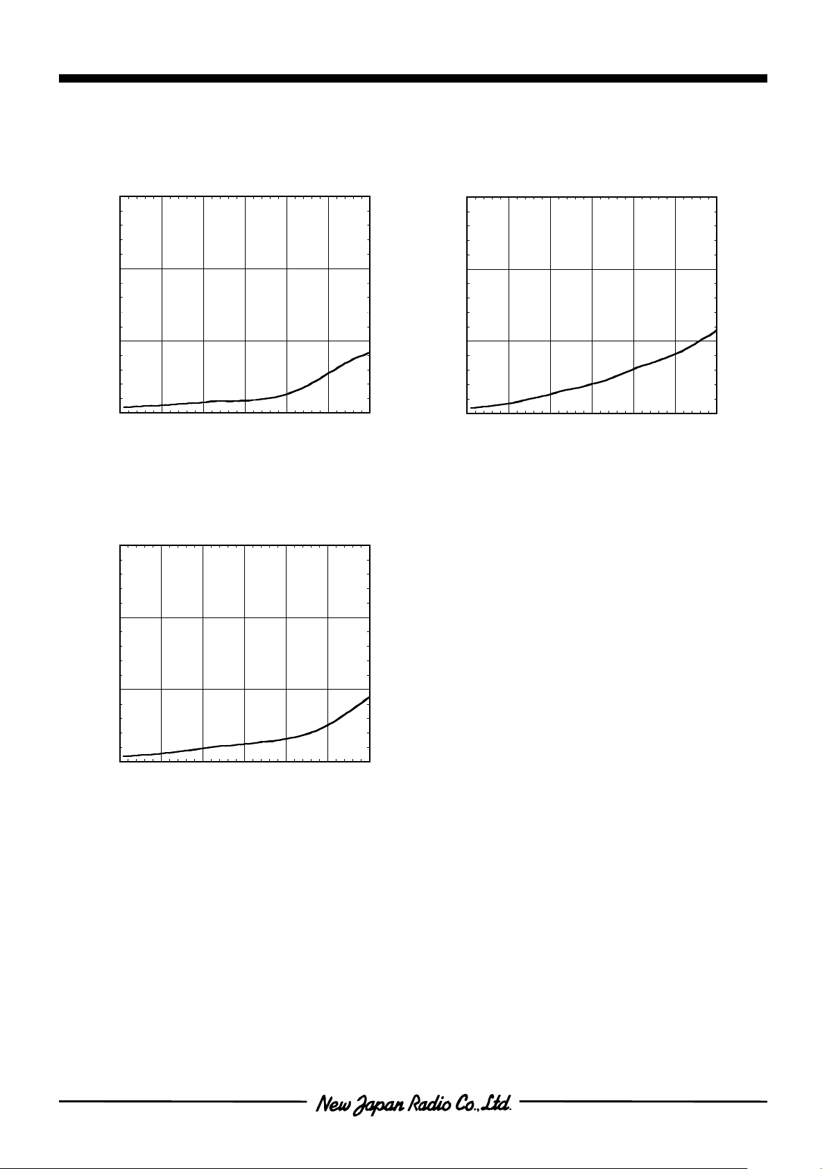
Switching Speed
(VCTL=2.7V,Pin=10dBm)
Page 15

NJG1524PC1
- 15 -
n
TYPICAL CHARACTERISTICS (Parts Table3)
-0.8
-0.7
-0.6
-0.5
-0.4
-0.3
-0.2
-50 0 50 100
Insertion Loss vs. Ambient Temperature
VCTL=2.5V
VCTL=2.7V
VCTL=3.0V
VCTL=3.5V
VCTL=4.0V
VCTL=5.0V
VCTL=6.0V
Insertion Loss (dB)
Ambient Temperature (oC)
(PC1-PA1,f=1GHz,Pin=0dBm)
-0.8
-0.7
-0.6
-0.5
-0.4
-0.3
-0.2
-50 0 50 100
Insertion Loss vs. Ambient Temperature
VCTL=2.5V
VCTL=2.7V
VCTL=3.0V
VCTL=3.5V
VCTL=4.0V
VCTL=5.0V
VCTL=6.0V
Insertion Loss (dB)
Ambient Temperature (oC)
(PC1-PA2,f=1GHz,Pin=0dBm)
-0.8
-0.7
-0.6
-0.5
-0.4
-0.3
-0.2
-50 0 50 100
Insertion Loss vs. Ambient Temperature
VCTL=2.5V
VCTL=2.7V
VCTL=3.0V
VCTL=3.5V
VCTL=4.0V
VCTL=5.0V
VCTL=6.0V
Insertion Loss (dB)
Ambient Temperature (oC)
(PC1-PA1,f=2GHz,Pin=0dBm)
-0.8
-0.7
-0.6
-0.5
-0.4
-0.3
-0.2
-50 0 50 100
Insertion Loss vs. Ambient Temperature
VCTL=2.5V
VCTL=2.7V
VCTL=3.0V
VCTL=3.5V
VCTL=4.0V
VCTL=5.0V
VCTL=6.0V
Insertion Loss (dB)
Ambient Temperature (oC)
(PC1-PA2,f=2GHz,Pin=0dBm)
-45
-40
-35
-30
-25
-20
-50 0 50 100
PC1-PA1 Isolation vs. Ambient Temperature
VCTL=2.5V
VCTL=2.7V
VCTL=3.0V
VCTL=3.5V
VCTL=4.0V
VCTL=5.0V
VCTL=6.0V
Isolation (dB)
Ambient Temperature (oC)
(VCTL1=0V ,VCTL2=2.7V ,f=1GHz,Pin=0dBm)
-55
-50
-45
-40
-35
-30
-50 0 50 100
PC1-PA1 Isolation vs. Ambient Temperature
VCTL=2.5V
VCTL=2.7V
VCTL=3.0V
VCTL=3.5V
VCTL=4.0V
VCTL=5.0V
VCTL=6.0V
Isolation (dB)
Ambient Temperature (oC)
(VCTL1=0V ,VCTL2=2.7V ,f=2GHz,Pin=0dBm)
Page 16

NJG1524PC1
- 16 -
n
TYPICAL CHARACTERISTICS (Parts Table3)
-45
-40
-35
-30
-25
-20
-50 0 50 100
PC1-PA2 Isolation vs. Ambient Temperature
VCTL=2.5V
VCTL=2.7V
VCTL=3.0V
VCTL=3.5V
VCTL=4.0V
VCTL=5.0V
VCTL=6.0V
Isolation (dB)
Ambient Temperature (oC)
(VCTL1=2.7V ,VCTL2=0V ,f=1GHz,Pin=0dBm)
-45
-40
-35
-30
-25
-20
-50 0 50 100
PC1-PA2 Isolation vs. Ambient Temperature
VCTL=2.5V
VCTL=2.7V
VCTL=3.0V
VCTL=3.5V
VCTL=4.0V
VCTL=5.0V
VCTL=6.0V
Isolation (dB)
Ambient Temperature (oC)
(VCTL1=2.7V ,VCTL=0V ,f=2GHz,Pin=0dBm)
-45
-40
-35
-30
-25
-20
-50 0 50 100
PA1-PA2 Isolation vs. Ambient Temperature
VCTL=2.5V
VCTL=2.7V
VCTL=3.0V
VCTL=3.5V
VCTL=4.0V
VCTL=5.0V
VCTL=6.0V
Isolation (dB)
Ambient Temperature (oC)
(VCTL1=2.7V ,VCTL2=0V ,f=1GHz,Pin=0dBm)
-45
-40
-35
-30
-25
-20
-50 0 50 100
PA1-PA2 Isolation vs. Ambient Temperature
VCTL=2.5V
VCTL=2.7V
VCTL=3.0V
VCTL=3.5V
VCTL=4.0V
VCTL=5.0V
VCTL=6.0V
Isolation (dB)
Ambient Temperature (oC)
(VCTL1=2.7V ,VCTL2=0V ,f=2GHz,Pin=0dBm)
-60
-55
-50
-45
-40
-35
-50 0 50 100
PC1-PC2 Isolation vs. Ambient Temperature
VCTL=2.5V
VCTL=2.7V
VCTL=3.0V
VCTL=3.5V
VCTL=4.0V
VCTL=5.0V
VCTL=6.0V
Isolation (dB)
Ambient Temperature (oC)
(VCTL1=2.7V ,VCTL2=0V ,f=2GHz,Pin=0dBm)
Page 17

NJG1524PC1
- 17 -
n
TYPICAL CHARACTERISTICS (Parts Table3)
1.0
1.1
1.2
1.3
1.4
1.5
-50 0 50 100
PC1-PA1(on) VSWR vs. Ambient Temperarure
VCTL=2.5V
VCTL=2.7V
VCTL=3.0V
VCTL=3.5V
VCTL=4.0V
VCTL=5.0V
VCTL=6.0V
VSWR
Ambient Temperature (oC)
(f=2.0GHz ,Pin=0dBm ,PC1 port)
1.0
1.1
1.2
1.3
1.4
1.5
-50 0 50 100
PC1-PA1(on) VSWR vs. Ambient Temperarure
VCTL=2.5V
VCTL=2.7V
VCTL=3.0V
VCTL=3.5V
VCTL=4.0V
VCTL=5.0V
VCTL=6.0V
VSWR
Ambient Temperature (oC)
(f=2.0GHz ,Pin=0dBm ,PA1 port)
1.0
1.1
1.2
1.3
1.4
1.5
-50 0 50 100
PC1-PA2(on) VSWR vs. Ambient Temperarure
VCTL=2.5V
VCTL=2.7V
VCTL=3.0V
VCTL=3.5V
VCTL=4.0V
VCTL=5.0V
VCTL=6.0V
VSWR
Ambient Temperature (oC)
(f=2.0GHz ,Pin=0dBm ,PC1 port)
1.0
1.1
1.2
1.3
1.4
1.5
-50 0 50 100
PC1-PA2(on) VSWR vs. Ambient Temperarure
VCTL=2.5V
VCTL=2.7V
VCTL=3.0V
VCTL=3.5V
VCTL=4.0V
VCTL=5.0V
VCTL=6.0V
VSWR
Ambient Temperature (oC)
(f=2.0GHz ,Pin=0dBm ,PA2 port)
1.0
1.1
1.2
1.3
1.4
1.5
-50 0 50 100
PC2-PB1(on) VSWR vs. Ambient Temperarure
VCTL=2.5V
VCTL=2.7V
VCTL=3.0V
VCTL=3.5V
VCTL=4.0V
VCTL=5.0V
VCTL=6.0V
VSWR
Temperature (oC)
(f=2.0GHz ,Pin=0dBm ,PC2 port)
1.0
1.1
1.2
1.3
1.4
1.5
-50 0 50 100
PC2-PB1(on) VSWR vs. Ambient Temperarure
VCTL=2.5V
VCTL=2.7V
VCTL=3.0V
VCTL=3.5V
VCTL=4.0V
VCTL=5.0V
VCTL=6.0V
VSWR
Ambient Temperature (oC)
(f=2.0GHz ,Pin=0dBm ,PB1 port)
Page 18

NJG1524PC1
- 18 -
n
TYPICAL CHARACTERISTICS (Parts Table3)
1.0
1.1
1.2
1.3
1.4
1.5
-50 0 50 100
PC2-PB2(on) VSWR vs. Ambient Temperarure
VCTL=2.5V
VCTL=2.7V
VCTL=3.0V
VCTL=3.5V
VCTL=4.0V
VCTL=5.0V
VCTL=6.0V
VSWR
Temperature (oC)
(f=2.0GHz ,Pin=0dBm ,PC2 port)
1.0
1.1
1.2
1.3
1.4
1.5
-50 0 50 100
PC2-PB2(on) VSWR vs. Ambient Temperarure
VCTL=2.5V
VCTL=2.7V
VCTL=3.0V
VCTL=3.5V
VCTL=4.0V
VCTL=5.0V
VCTL=6.0V
VSWR
Ambient Temperature (oC)
(f=2.0GHz ,Pin=0dBm ,PB2 port)
10
20
30
40
50
60
-50 0 50 100
Control Current vs. Ambient Temperature
VCTL=2.5V
VCTL=2.7V
VCTL=3.0V
VCTL=3.5V
VCTL=4.0V
VCTL=5.0V
VCTL=6.5V
Control Current (uA)
Ambient Temperature (oC)
( PC1-PA1 ,f=1GHz ,Pin=10dBm )
10
20
30
40
50
60
-50 0 50 100
Control Current vs. Ambient Temperature
VCTL=2.5V
VCTL=2.7V
VCTL=3.0V
VCTL=3.5V
VCTL=4.0V
VCTL=5.0V
VCTL=6.5V
Control Current (uA)
Ambient Temperature (oC)
( PC1-PA2 ,f=1GHz ,Pin=10dBm )
18
20
22
24
26
28
-50 0 50 100
P-1dB vs. Ambient Temperature
VCTL=2.5V
VCTL=2.7V
VCTL=3.0V
VCTL=3.5V
P-1dB (dBm)
Ambient Temperature (oC)
(PC1-PA1 ,f=2GHz)
18
20
22
24
26
28
-50 0 50 100
P-1dB vs. Ambient Temperature
VCTL=2.5V
VCTL=2.7V
VCTL=3.0V
VCTL=3.5V
P-1dB (dBm)
Ambient Temperature (oC)
(PC1-PA2 ,f=2GHz)
Page 19

NJG1524PC1
- 19 -
n
APPLICATION CIRCUIT
n
RECOMMENDED PCB DESIGN
PRCAUTION
[1] The DC blocking capacitor have to be placed at RF terminal of PC1, PC2, PA1, PA2, PB1,
PB2.
Please choose appropriate capacitance values to the application frequency.
[2]To reduce stlipline influence on RF characteristics, please locate bypass capacitors (C7, C8)
close to each terminal.
[3]For good isolation the GND terminal must be placed possibly close to ground place of
substrate, and through holes for GND should be placed near by the pin connection.
PCB SIZE=26x26mm
PCB: FR-4,t=0.5mm
CAPACITOR: size 1005
Strip line width=1.0mm
Parts table
Parts ID
1 2 3
fin=50100MHz
fin=0.1-
0.5GHz
fin=0.5-
2.5GHz
C1~C6 0.01uF 1000pF 56pF
C7,C8 10pF 10pF 10pF
C1
C3
C2
C5
C7
C4
C6
C8
PA1
PB2
PB1
PA2
PC1
PC2
V
CTL1
V
CTL2
Page 20

NJG1524PC1
- 20 -
n
PACKAGE OUTLINE (FFP16-C1)
0.85±0.15
0.10
0.300.500.50
0.365 0.27
2.5±0.1
0.30
0.20
2pin INDEX
1pin INDEX
0.17
0.254±0.1
0.35
UNIT : mm
PCB : Ceramic
OVER COAT : Epoxy resin
TERMINAL TREAT : Au
Cautions on using this product
This product contains Gallium-Arsenide (GaAs) which is a harmful material.
• Do NOT eat or put into mouth.
• Do NOT dispose in fire or break up this product.
• Do NOT chemically make gas or powder with this product.
• To waste this product, please obey the relating law of your country.
This product may be damaged with electric static discharge (ESD) or spike voltage. Please handle with
care to avoid these damages.
[CAUTION]
The specifications on this databook are only
given for information , without any guarantee
as regards either mistakes or omissions. The
application circuits in this databook are
described only to show representative usages
of the product and not intended for the
guarantee or permission of any right including
the industrial rights.
 Loading...