

Page 1
NJG1518KB2
- 1 -
SPDT SWITCH GaAs MMIC
n
GENERAL DESCRIPTION
n
PACKAGE OUTLINE
NJG1518KB2 is a SPDT switch IC featured low insertion
loss, medium handling power and high isolation. This device
is suitable for switching of Tx/Rx signals at sub-microwave
applications.
This switch exhibits wide frequency range from 50MHz to
3.0GHz at low operating voltage of 2.5V, and is operated up
to 25dBm at 3.0V operating voltage.
The ultra small & ultra thin FLP6 package is applied.
n
FEATURES
lSingle low voltage control +2.5~6.5V
lLow insertion loss 0.4dB typ. @f=1GHz, Pin=22dBm
0.5dB typ. @f=2GHz, Pin=22dBm
lHandling power 23dBm max. @f=2GHz, V
CTL
=2.7V
34.5dBm max. @f=2GHz, V
CTL
=6.5V
lHigh isolation 28dB typ. @f=1GHz, Pin=22dBm
lLow current consumption 6uA typ. @f=2GHz, Pin=22dBm, R1=560kΩ
lUltra small & ultra thin package FLP6-B2 (Mount Size: 2.1x2.0x0.75mm)
n
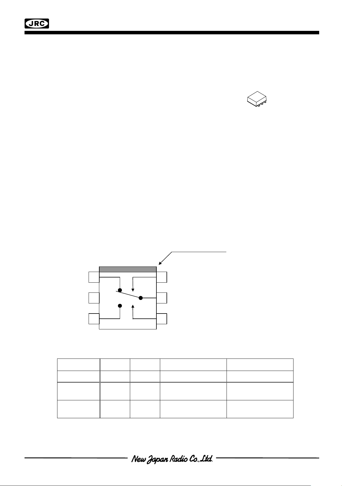
PIN CONFIGURATION
n
TRUTH TABLE
V
CTL1
H L L H
V
CTL2
L H L H
P1 - PC ON OFF
Insertion Loss=14dB
P1 return Loss=-3dB
Insertion Loss=14dB
P1 return Loss=-2dB
P2 - PC OFF ON
Insertion Loss=14dB
P2 return Loss=-3dB
Insertion Loss=14dB
P2 return Loss=-2dB
“H”=V
CTL (H),
“L”=V
CTL (L)
Note: The values of insertion losses and return losses are typical values at 2.0GHz.
NJG1518KB2
KB2 Type
(Top View)
3
2
1
4
5
6
PIN Connection
1. P1
2. EXTCAP
3. P2
4. V
CTL2
5. PC
6. V
CTL1
Orientation Mark
Page 2
NJG1518KB2
- 2 -
n
ABSOLUTE MAXIMUM RATINGS
(Ta=25°C)
PARAMETERS SYMBOL CONDITIONS RATINGS UNITS
Input Power P
in
V
CTL (L)
=0V, V
CTL (H)
=2.7V 32 dBm
Control Voltage V
CTL
V
CTL (H)-VCTL (L)
7.5 V
Power Dissipation P
D
450 mW
Operating Temp. T
opr
-30~+85 °C
Storage Temp. T
stg
-55~+125 °C
n
ELECTRICAL CHARACTERISTICS
(V
CTL (L)
=0V, V
CTL (H)
=2.7V ZS=Zl=50Ω, R1=560kΩ, C6=10pF, Ta=25°C)
PARAMETERS SYMBOL CONDITIONS MIN TYP MAX UNITS
Control voltage (Low) V
CTL (L)
-0.2 0 0.2 V
Control voltage (High) V
CTL (H)
2.5 2.7 6.5 V
Control current * I
CTL
f=2.0GHz, Pin=22dBm - 6 10 uA
Insertion loss 1 LOSS1 f=1.0GHz, Pin=22dBm - 0.4 0.7 dB
Insertion loss 2 LOSS2 f=2.0GHz, Pin=22dBm - 0.5 0.8 dB
Isolation 1
(PC-P1, PC-P2, P1-P2)
ISL1 f=1.0GHz, Pin=22dBm 26 28 - dB
Isolation 2
(PC-P1, PC-P2, P1-P2)
ISL2
f=2.0GHz, Pin=22dBm,
C6=5pF
23 25 - dB
Maximum Input Power 1** P
in1
V
CTL (H)
=2.7V, f=2.0GHz - - 23.0 dBm
Maximum Input Power 2** P
in2
V
CTL (H)
=3.0V, f=2.0GHz - - 24.0 dBm
Maximum Input Power 3** P
in3
V
CTL (H)
=6.5V, f=2.0GHz - - 34.5 dBm
Pin at 1dB
compression point
P
-1dB
f=2.0GHz 27 30 - dBm
VSWR (PC, P1, P2) VSWR f=0.05~2.2GHz, ON State - 1.3 1.6
Switching time T
SW
f=0.05~2.5GHz - 35 - ns
* The control current I
CTL
depends on the resistance of R1. Smaller resistance of R1 makes larger control current.
** Maximum input power: This value is defined as maximum input power of linear or damage free operation.
Page 3
NJG1518KB2
- 3 -
n
TERMINAL INFORMATION
No. SYMBOL EXPLANATION
1 P1
RF port. This port is connected with PC port by controlling 6th pin (V
CTL (H)
)
to 2.5~6.5V and 4th pin(V
CTL (L)
) to -0.2~+0.2V. An external capacitor is
required to block the DC bias voltage of internal circuit. (50~100MHz:
0.01uF, 0.1~0.5GHz: 1000pF, 0.5~2.5GHz: 56pF)
2 EXTCAP
External capacitor terminal. The isolation characteristics depends on the
value of the capacitor which connected with GND. An external capacitor is
required to block the DC bias voltage of internal circuit. (50MHz~1.7GHz:
10pF, 1.7~2.5GHz: 5pF)
3 P2
RF port. This port is connected with PC port by controlling 4th pin (V
CTL (H)
)
to 2.5 – 6.5V and 6th pin(V
CTL (L)
) to -0.2~+0.2V. In order to block the DC
bias voltage of internal circuit, an external capacitor is required.
(50~100MHz: 0.01uF, 0.1~0.5GHz: 1000pF, 0.5~2.5GHz: 56pF)
4 V
CTL2
Control port 2. The voltage of this port controls PC to P2 state. The ‘ON’
and ‘OFF’ state is toggled by controlling voltage of this terminal such as
high-state (2.5~6.5V) or low-state (-0.2~+0.2V). The voltage of 6th pin
have to be set to opposite state. The bypass capacitor has to be chosen
to reduce switching time delay from 10pF~1000pF range.
5 PC
Common RF port. In order to block the DC bias voltage of internal circuit,
an external capacitor is required. (50~100MHz: 0.01uF, 0.1~0.5GHz:
1000pF, 0.5~2.5GHz: 56pF)
6 V
CTL1
Control port 1. The voltage of this port controls PC to P2 state. The ‘ON’
and ‘OFF’ state is toggled by controlling voltage of this terminal such as
high-state (2.5~6.5V) or low-state (-0.2~+0.2V). The voltage of 4th pin
have to be set to opposite state. The bypass capacitor has to be chosen
to reduce switching time delay from 10pF~1000pF range.
Page 4
NJG1518KB2
- 4 -
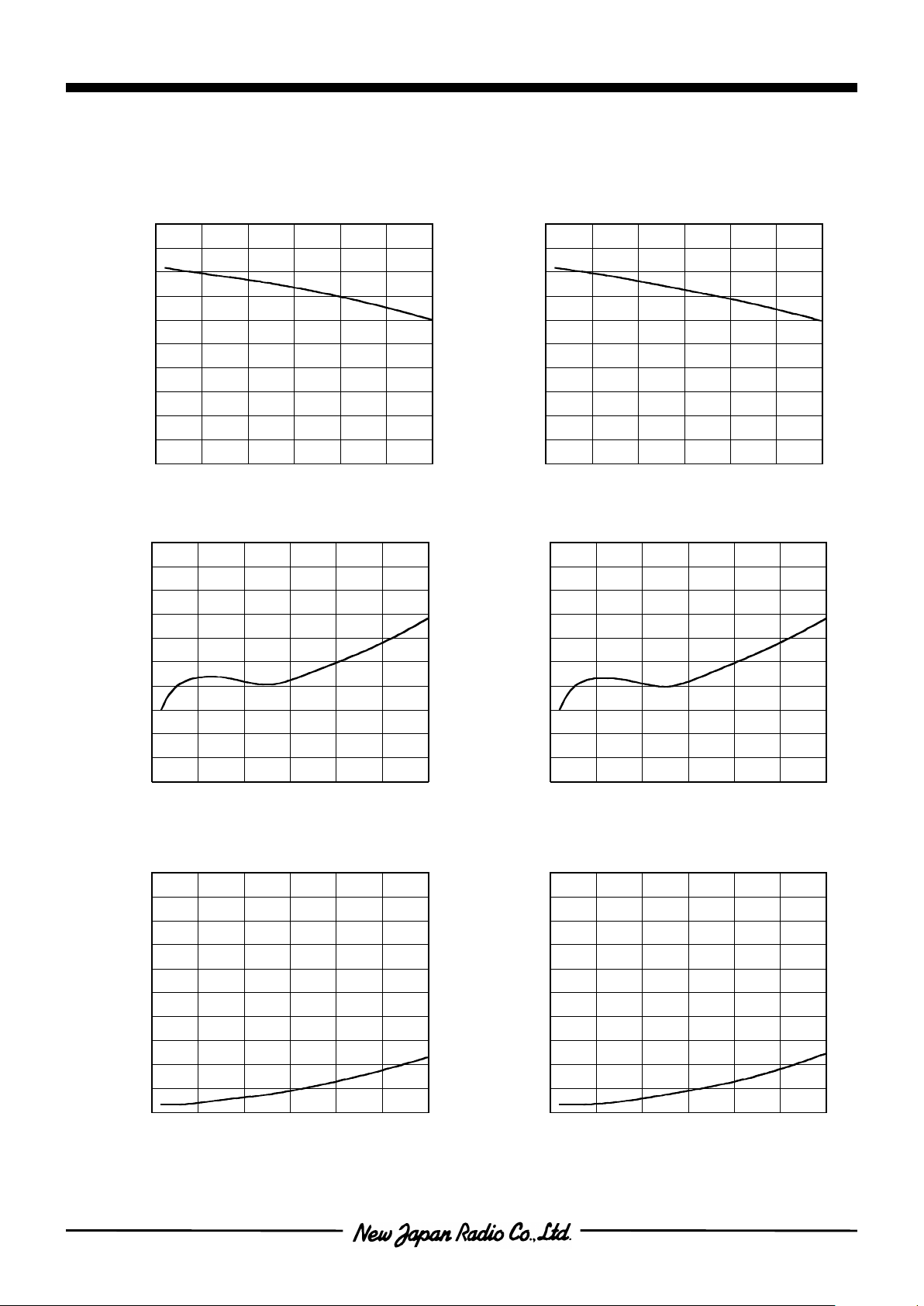
-50
-40
-30
-20
-10
0
0 0.5 1 1.5 2 2.5 3
Isolation (dB)
Frequency (GHz)
PC-P1 Isolation vs. Frequency
(V
CTL1
=0V,V
CTL2
=2.7V,Pin=0dBm)
-50
-40
-30
-20
-10
0
0 0.5 1 1.5 2 2.5 3
Isolation (dB)
Frequency (GHz)
PC-P2 Isolation vs. Frequency
(V
CTL1
=2.7V,V
CTL2
=0V,Pin=0dBm)
-2
-1.6
-1.2
-0.8
-0.4
0
0 0.5 1 1.5 2 2.5 3
Insertion Loss (dB)
Frequency (GHz)
PC-P1 Insertion Loss vs. Frequency
(V
CTL1
=2.7V,V
CTL2
=0V,Pin=0dBm)
-2
-1.6
-1.2
-0.8
-0.4
0
0 0.5 1 1.5 2 2.5 3
Insertion Loss (dB)
Frequency (GHz)
PC-P2 Insertion Loss vs. Frequency
(V
CTL1
=0V,V
CTL2
=2.7V,Pin=0dBm)
1
1.4
1.8
2.2
2.6
3
0 0.5 1 1.5 2 2.5 3
VSWR
Frequency (GHz)
PC-P1 VSWR vs. Frequency
(V
CTL1
=2.7V,V
CTL2
=0V,PC port)
1
1.4
1.8
2.2
2.6
3
0 0.5 1 1.5 2 2.5 3
VSWR
Frequency (GHz)
P1-PC VSWR vs. Frequency
(V
CTL1
=2.7V,V
CTL2
=0V,P1 port)
n
ELECTRICAL CHARACTERISTICS
(0.1GHz~3GHz, with application circuit, R1=560kΩ, C6=10pF, Losses of external circuit are excluded)
Page 5

NJG1518KB2
- 5 -
20
25
30
35
-50 0 50 100
V
CTL(H)
=2.5V
V
CTL(H)
=2.7V
V
CTL(H)
=3.0V
V
CTL(H)
=3.5V
V
CTL(H)
=5.0V
V
CTL(H)
=6.5V
Isolation (dB)
Ambient Temperature (oC)
Isolation vs. Ambient Temperature
(PC-P1 port,fin=1GHz,V
CTL(L)
=0V)
0
10
20
30
40
50
-50 0 50 100
V
CTL(H)
=2.5V
V
CTL(H)
=2.7V
V
CTL(H)
=3.0V
V
CTL(H)
=3.5V
V
CTL(H)
=5.0V
V
CTL(H)
=6.5V
Control Current (uA)
Ambient Temperature (oC)
I
CTL
vs. Ambient Temperature
(PC-P1 port,fin=1GHz,V
CTL(L)
=0V)
1
1.4
1.8
2.2
2.6
3
0 0.5 1 1.5 2 2.5 3
VSWR
Frequency (GHz)
P2-PC VSWR vs. Frequency
(V
CTL1
=0V,V
CTL2
=2.7V,P2 port)
10
15
20
25
30
35
4
5
6
7
8
9
10 15 20 25 30 35
Pout
P-1dB
ICTL
Output Power (dBm)
I
CTL
(uA)
Input Power (dBm)
Pin vs. Pout&I
CTL
(fin=2GHz,V
CTL(H)
=2.7V,V
CTL(L)
=0V)
P-1dB=30.5dBm
0
0.2
0.4
0.6
0.8
1
-50 0 50 100
V
CTL(H)
=2.5V
V
CTL(H)
=2.7V
V
CTL(H)
=3.0V
V
CTL(H)
=3.5V
V
CTL(H)
=5.0V
V
CTL(H)
=6.5V
Insertion Loss (dB)
Ambient Temperature (oC)
Insertion Loss vs. Ambient Temperature
(PC-P1 port,fin=1GHz,V
CTL(L)
=0V)
n
ELECTRICAL CHARACTERISTICS
(with application circuit, without DC Blocking Capacitor, Losses of external circuit are excluded)
36.2ns
V
CTL
RF
C4, C5=10pF, V
CTL (H)
=2.7V, V
CTL (L)
=0V, P
i n
=0dBm
Switching Speed
Trig’d
625mV
100mV
/div
-375mV
-13.8nF 86.2nF10ns/div
Page 6

NJG1518KB2
- 6 -
-2
-1.6
-1.2
-0.8
-0.4
0
50 60 70 80 90 100
Insertion Loss (dB)
Frequency (MHz)
PC-P2 Insertion Loss vs. Frequency
(V
CTL1
=0V,V
CTL2
=2.7V,Pin=0dBm)
-2
-1.6
-1.2
-0.8
-0.4
0
50 60 70 80 90 100
Insertion Loss (dB)
Frequency (MHz)
PC-P1 Insertion Loss vs. Frequency
(V
CTL1
=2.7V,V
CTL2
=0V,Pin=0dBm)
-50
-40
-30
-20
-10
0
50 60 70 80 90 100
Isolation (dB)
Frequency (MHz)
PC-P1 Isolation vs. Frequency
(V
CTL1
=0V,V
CTL2
=2.7V,Pin=0dBm)
-50
-40
-30
-20
-10
0
50 60 70 80 90 100
Isolation (dB)
Frequency (MHz)
PC-P2 Isolation vs. Frequency
(V
CTL1
=2.7V,V
CTL2
=0V,Pin=0dBm)
1
1.4
1.8
2.2
2.6
3
50 60 70 80 90 100
VSWR
Frequency (MHz)
PC-P1 VSWR vs. Frequency
(V
CTL1
=2.7V,V
CTL2
=0V,PC port)
1
1.4
1.8
2.2
2.6
3
50 60 70 80 90 100
VSWR
Frequency (MHz)
P1-PC VSWR vs. Frequency
(V
CTL1
=2.7V,V
CTL2
=0V,P1 port)
n
ELECTRICAL CHARACTERISTICS
(50MHz~100MHz,with Application circuit (Parts list 1), Losses of PCB, connector and DC blocking capacitor are included)
Page 7

NJG1518KB2
- 7 -
-2
-1.6
-1.2
-0.8
-0.4
0
100 150 200 250 300 350 400 450 500
Insertion Loss (dB)
Frequency (MHz)
PC-P1 Insertion Loss vs. Frequency
(V
CTL1
=2.7V,V
CTL2
=0V,Pin=0dBm)
-2
-1.6
-1.2
-0.8
-0.4
0
100 150 200 250 300 350 400 450 500
Insertion Loss (dB)
Frequency (MHz)
PC-P2 Insertion Loss vs. Frequency
(V
CTL1
=0V,V
CTL2
=2.7V,Pin=0dBm)
n
ELECTRICAL CHARACTERISTICS
(100MHz~500MHz, with Application circuit (Parts list 2), Losses of PCB, connector and DC blocking capacitor are included)
-50
-40
-30
-20
-10
0
100 150 200 250 300 350 400 450 500
Isolation (dB)
Frequency (MHz)
PC-P1 Isolation vs. Frequency
(V
CTL1
=0V,V
CTL2
=2.7V,Pin=0dBm)
-50
-40
-30
-20
-10
0
100 150 200 250 300 350 400 450 500
Isolation (dB)
Frequency (MHz)
PC-P2 Isolation vs. Frequency
(V
CTL1
=2.7V,V
CTL2
=0V,Pin=0dBm)
1
1.4
1.8
2.2
2.6
3
100 150 200 250 300 350 400 450 500
VSWR
Frequency (MHz)
PC-P1 VSWR vs. Frequency
(V
CTL1
=2.7V,V
CTL2
=0V,PC port)
1
1.4
1.8
2.2
2.6
3
100 150 200 250 300 350 400 450 500
VSWR
Frequency (MHz)
P1-PC VSWR vs. Frequency
(V
CTL1
=2.7V,V
CTL2
=0V,P1 port)
Page 8

NJG1518KB2
- 8 -
-2
-1.6
-1.2
-0.8
-0.4
0
0 0.5 1 1.5 2 2.5 3
Insertion Loss (dB)
Frequency (GHz)
PC-P1 Insertion Loss vs. Frequency
(V
CTL1
=2.7V,V
CTL2
=0V,Pin=0dBm)
-2
-1.6
-1.2
-0.8
-0.4
0
0 0.5 1 1.5 2 2.5 3
Insertion Loss (dB)
Frequency (GHz)
PC-P2 Insertion Loss vs. Frequency
(V
CTL1
=0V,V
CTL2
=2.7V,Pin=0dBm)
n
ELECTRICAL CHARACTERISTICS
(0.1GHz~3GHz,with Application circuit (Parts list 3), Losses of PCB, connector and DC blocking capacitor are included)
-50
-40
-30
-20
-10
0
0 0.5 1 1.5 2 2.5 3
Isolation (dB)
Frequency (GHz)
PC-P1 Isolation vs. Frequency
(V
CTL1
=0V,V
CTL2
=2.7V,Pin=0dBm)
-50
-40
-30
-20
-10
0
0 0.5 1 1.5 2 2.5 3
Isolation (dB)
Frequency (GHz)
PC-P2 Isolation vs. Frequency
(V
CTL1
=2.7V,V
CTL2
=0V,Pin=0dBm)
Page 9

NJG1518KB2
- 9 -
n
ELECTRICAL CHARACTERISTICS
(0.1GHz~3GHz,with Application circuit (Parts list 4), Losses of PCB, connector and DC blocking capacitor are included)
-50
-40
-30
-20
-10
0
0 0.5 1 1.5 2 2.5 3
Isolation (dB)
Frequency (GHz)
PC-P1 Isolation vs. Frequency
(V
CTL1
=0V,V
CTL2
=2.7V,Pin=0dBm)
-50
-40
-30
-20
-10
0
0 0.5 1 1.5 2 2.5 3
Isolation (dB)
Frequency (GHz)
PC-P2 Isolation vs. Frequency
(V
CTL1
=2.7V,V
CTL2
=0V,Pin=0dBm)
Page 10

NJG1518KB2
- 10 -
n
ELECTRICAL CHARACTERISTICS
(Losses of PCB, connector and DC blocking capacitor at each frequency.)
-2
-1.6
-1.2
-0.8
-0.4
0
50 60 70 80 90 100
Insertion Loss (dB)
Frequency (MHz)
PCB Through Loss vs. Frequency
(Frequency:50MHz-100MHz)
-2
-1.6
-1.2
-0.8
-0.4
0
100 150 200 250 300 350 400 450 500
Insertion Loss (dB)
Frequency (MHz)
PCB Through Loss vs. Frequency
(Frequency:100MHz-500MHz)
-2
-1.6
-1.2
-0.8
-0.4
0
0 0.5 1 1.5 2 2.5 3
Insertion Loss (dB)
Frequency (GHz)
PCB Through Loss vs. Frequency
(Frequency:100MHz-3GHz)
Page 11

NJG1518KB2
- 11 -
n
APPLICATION CIRCUIT
n
RECOMMENDED PCB DESIGN
PRECAUTIONS
[1]The DC blocking capacitors have to be placed at RF terminal of P1, P2 and PC. Please
choose appropriate capacitance values to the application frequency.
[2]To reduce stripline influence on RF characteristics, please locate bypass capacitors (C4, C5)
close to each terminal.
[3]For good isolation, the GND terminal (2nd pin) must be placed possibly close to ground plane
of substrate, and through holes for GND should be placed near by the pin connection.
Parts number List 1 List 2 List 3 List 4
fin=50~100MHz fin=0.1~0.5GHz fin=0.5~1.7GHz fin=1.7~2.5GHz
C1~C3 0.01uF 1000pF 56pF 56pF
C4, C5 10pF 10pF 10pF 10pF
C6 10pF 10pF 10pF 5pF
R1 560kΩ 560kΩ 560kΩ 560kΩ
Parts List
Zo=50Ω
3
214
56PC
P2
P1
V
CTL1
(2.7V/0V)
C1
C3
C5
C2
C4
NJG1518KB2
C6
R1
Zo=50Ω
Zo=50Ω
V
CTL2
(0V/2.7V)
(TOP VIEW)
P2
P1
PC
V
CTL1
V
CTL2
C3
C2
C5
C4
C1
R1
C6
PCB SIZE=19.4x14.0mm
PCB: FR-4, t=0.2mm
CAPACITOR: size 1005
STRIPLINE WIDTH=0.4mm
Page 12

NJG1518KB2
- 12 -
n
PACKAGE OUTLINE (FLP6-B2)
Cautions on using this product
This product contains Gallium-Arsenide (GaAs) which is a harmful material.
• Do NOT eat or put into mouth.
• Do NOT dispose in fire or break up this product.
• Do NOT chemically make gas or powder with this product.
• To waste this product, please obey the relating law of your country.
This product may be damaged with electric static discharge (ESD) or spike voltage. Please handle
with care to avoid these damages.
[CAUTION]
The specifications on this databook are only
given for information , without any guarantee
as regards either mistakes or omissions. The
application circuits in this databook are
described only to show representative usages
of the product and not intended for the
guarantee or permission of any right including
the industrial rights.
Lead material : Copper
Lead surface finish : Solder plating
Molding material : Epoxy resin
UNIT : mm
Weight : 6.5mg
2.0±0.1
6 5 4
1 2 3
0.20.2
2.1±0.1
1.7±0.1
0.65 0.65
0.75±0.05
+0.1
0.2-0.05
+0.1
0.1 0.1
0.15-0.05
 Loading...