

NJG1515AVB2
- 1 -
TDMA ANTENNA SWITCH GaAs MMIC
n
GENERAL DESCRIPTION
NJG1515AVB2 is an antenna switch IC for a digital cellular
phone of 800MHz and 1.5GHz band.
The parallel control signals of three bits connect T/R circuits
to internal two antennas or external two antennas.
The termination ports with external matching circuits make
low interference between diversity antennas.
NJG1515AVB2 features very low insertion loss and low
current consumption in a very small SSOP20 package.
n
FEATURES
lLow voltage operation -2.5V (Tx only) and +3.5V
lLow current consumption 10uA typ. @Pin=30dBm (Transmit)
2uA typ. @Pin=10dBm (Receiving)
lLow insertion loss 0.5dB typ. @(TX-ANT1, TX-EXT1) f=940MHz, Pin=30dBm
0.6dB typ. @(TX-ANT1, TX-EXT1) f=1453MHz, Pin=30dBm
lLow Adjacent Channel -63dBc typ. @VDD=+3.5V, VSS=-2.5V, f=940MHz, Pin=30dBm
Leakage Power -64dBc typ. @VDD=+3.5V, VSS=-2.5V, f=1453MHz, Pin=30dBm
lPackage SSOP20-B2 (Mount Size: 6.4x5.0x1.25mm)
n
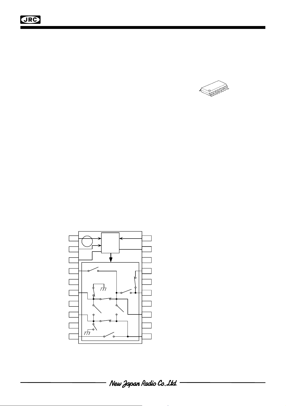
PACKAGE OUTLINE
NJG1515AVB2
n
PIN CONFIGURATION
VB2 Type
(Top View)
1
2
3
4
5
6
7
8
9
10
ANT-SW
DECORDER
20
Pin Connection
19
18
17
16
15
14
13
12
11
1. CTL2
2. CTL3
3. V
SS
4. EXT2
5. GND
6. EXT1
7. GND
8. TX
9. GND
10. TER2
11. ANT1
12. GND
13. RX
14. GND
15. ANT2
16. GND
17. TER1
18. GND
19. V
DD
20. CTL1
NJG1515AVB2
- 2 -
nABSOLUTE MAXIMUM RATINGS
CTL (H)
PARAMETER SYMBOL CONDITIONS RATINGS UNITS
(T
a
=25°C)
Supply voltage 1 V
Supply voltage 2 V
Control voltage V
DD
SS
CTR
VDD Terminal 6.0 V
VSS Terminal -4.0 V
CTL1, CTL2, CTL3
Each Terminals
TX, ANT1, EXT1 Terminals 37 dBm
Input power P
in
RX, ANT2, EXT2 Terminals 28 dBm
Power dissipation P
Operating temp. T
Storage temp. T
D
opr
stg
nELECTRICAL CHARACTERISTICS 1 [DC CHARACTERISTICS]
Common conditions: Ta=25°C, VDD=3.5V, VSS=-2.5V
TX, RX, ANT1, ANT2, EXT1, EXT2: terminated (50Ω)
TER1, TER2: connected to GND by 5pF capacitors
PARAMETER SYMBOL CONDITIONS MIN TYP MAX UNITS
Positive supply voltage V
Negative supply voltage V
DD
SS
VDD Terminal 2.7 3.5 5.0 V
VSS Terminal -3.5 -2.5 -2.0 V
6.0 V
600 mW
-40~85
-55~125
°C
°C
Current consumption 1 I
Current consumption 2 I
Current consumption 3 I
Current consumption 4 I
DD1
SS1
DD2
SS2
Control voltage (H) V
Control voltage (L) V
Control current I
Control terminal
Input Impedance
* The voltage of this terminal should be supplied before or same time with other DC supplying
terminals. (CTL1~3, VSS).
CTL (L)
CTL
R
in
VDD Terminal No RF Signal - 2.0 5.0 uA
VSS Terminal No RF Signal -0.1 - 0 uA
f=0.1~2GHz, Pin=30dBm
Transmitting state
f=0.1~2GHz, Pin=30dBm
Transmitting state
- 10 30 uA
-30 -10 - uA
CTL1, CTL2, CTL3 terminals 2.0 3.0 V
CTL1, CTL2, CTL3 terminals 0 0 0.6 V
CTL1, CTL2, CTL3=VDD
or CTL1, CTL2, CTL3=0V
CTL1, CTL2, CTL3
each Terminal
-1.3 - 1.3 uA
4 - -
DD
V
MΩ
NJG1515AVB2
- 3 -
nELECTRICAL CHARACTERISTICS 2 [800MHz TX Mode]
-0.5dB
f=960MHz, Ta=25°C, VDD=3.5V, VSS=-2.5V
Common Conditions:
Tested on PCB circuit as shown below.
Insertion loss of each connectors, striplines, and capacitors are excluded.
TX, RX, ANT1, ANT2, EXT1 and EXT2 are terminated to 50Ω.
TER1 and TER2 are connected to GND through 5pFcapacitor.
PARAMETER SYMBOL CONDITION MIN TYP MAX UNITS
Frequency range 1 fin1 885 - 960 MHz
TX-ANT1 Insertion Loss LOSS1 Pin=30dBm - 0.5 0.65 dB
TX-EXT1 Insertion Loss LOSS2 Pin=30dBm - 0.5 0.65 dB
TX-RX Isolation ISL1
TX-ANT1 Isolation ISL2
TX-ANT2 Isolation ISL3
TX-EXT1 Isolation ISL4
TX-EXT2 Isolation ISL5
Pin at 0.5dB
compression point 1
Adjacent Channel
Leakage Power 1
Adjacent Channel
Leakage Power 3
P
ACP1
ACP2
2nd Harmonics 1 2f0(1)
3rd Harmonics 1 3f0(1)
Pin=30dBm
TX-ANT1, TX-EXT1 passing
Pin=30dBm
TX-EXT1 passing
Pin=30dBm
TX-ANT1, TX-EXT1 passing
Pin=30dBm
TX-ANT1 passing
Pin=30dBm
TX-ANT1, TX-EXT1 passing
24 29 - dB
22 27 - dB
33 38 - dB
21 26 - dB
32 37 - dB
(1) TX-ANT1, TX-EXT1 passing 33 34 - dBm
PDC Standard, ±50kHz offset
Pin=30dBm, Input Signal
ACP=-64dBc @30dBm
PDC Standard, ±100kHz offset
Pin=30dBm, Input Signal
ACP=-76dBc @30dBm
Pin=30dBm, Input Signal 2nd
Harmonics=-68dBc
Pin=30dBm, Input Signal 2nd
Harmonics=-69dBc
- -63 -60 dBc
- -74 -70 dBc
- -63 -60 dBc
- -63 -60 dBc
VSWR1 VSWR1 TX-ANT1, TX-EXT1 passing - 1.3 1.5
Switching time TD1 CTL1~3 - 120 500 nsec
NJG1515AVB2
- 4 -
nELECTRICAL CHARACTERISTICS 3 [800MHz Rx Mode]
f=885MHz, Ta=25°C, VDD=3.5V, VSS=0V
Common Conditions:
Tested on PCB circuit as shown below
Insertion loss of each connectors, striplines, and capacitors are excluded.
TX, RX, ANT1, ANT2, EXT1 and EXT2 are terminated to 50Ω.
TER1 and TER2 are connected to GND through 5pFcapacitor.
PARAMETER SYMBOL CONDITIONS MIN TYP MAX UNITS
Frequency range 2 fin2 810 - 885 MHz
RX-ANT1 Insertion Loss LOSS3 Pin=10dBm - 0.65 0.80 dB
RX-ANT2 Insertion Loss LOSS4 Pin=10dBm - 0.60 0.75 dB
RX-EXT1 Insertion Loss LOSS5 Pin=10dBm - 0.70 0.85 dB
RX-EXT2 Insertion Loss LOSS6 Pin=10dBm - 0.65 .80 dB
RX-ANT1 Isolation ISL6
RX-ANT2 Isolation ISL7
RX-EXT1 Isolation ISL8
RX-EXT2 Isolation ISL9
Pin at 1dB
compression point 1
VSWR 2 VSWR2
Switching time 2 TD2 CTL1~3 - 120 500 nsec
P-1(1)
Pin=10dBm, RX-ANT2,
RX-EXT1, RX-EXT2 passing
Pin=10dBm, RX-ANT1,
RX-EXT1, RX-EXT2 passing
Pin=10dBm, RX-ANT1,
RX-ANT2, RX-EXT2 passing
Pin=10dBm, RX-ANT1,
RX-ANT2, RX-EXT1 passing
RX-ANT1, RX-ANT2,
RX-EXT1, RX-EXT2 passing
RX-ANT1, RX-ANT2,
RX-EXT1, RX-EXT2 passing
21 24 - dB
22 25 - dB
22 25 - dB
20 23 - dB
20 26 - dBm
- 1.4 1.6
NJG1515AVB2
- 5 -
nELECTRICAL CHARACTERISTICS 4 [1.5GHz Tx Mode]
-0.5dB
f=1453MHz, Ta=25°C, VDD=3.5V, VSS=-2.5V
Common Condition:
Tested on PCB circuit as shown below
Insertion loss of each connectors, striplines, and capacitors are excluded.
TX, RX, ANT1, ANT2, EXT1 and EXT2 are terminated to 50Ω.
TER1 and TER2 are connected to GND through 5pFcapacitor.
PARAMETER SYMBOL CONDITIONS MIN TYP MAX UNITS
Frequency range 3 fin3 1429 - 1453 MHz
TX-ANT1
Insertion Loss
TX-EXT1
Insertion Loss
TX-RX Isolation ISL10
TX-ANT1 Isolation ISL11
TX-ANT2 Isolation ISL12
TX-EXT1 Isolation ISL13
TX-EXT2 Isolation ISL14
Pin at 0.5dB
compression point 2
Adjacent channel
leakage power5
Adjacent channel
leakage power 7
2nd Harmonics 2 2f0(2)
3rd Harmonics 2 3f0(2)
LOSS7 Pin=30dBm - 0.55 0.70 dB
LOSS8 Pin=30dBm - 0.65 0.80 dB
P
ACP3
ACP4
Pin=30dBm
TX-ANT1, TX-EXT1 passing
Pin=30dBm
TX-EXT1 passing
Pin=30dBm
TX-ANT1, TX-EXT1 passing
Pin=30dBm
TX-ANT1 passing
Pin=30dBm
TX-ANT1, TX-EXT1 passing
(2) TX-ANT1, TX-EXT1 passing 33.5 35.5 - dBm
PDC Standard, ±50KHz offset
Pin=30dBm, Input Signal
ACP=-67dBc @ 30dBm
PDC Standard, ±100kHz offset
Pin=30dBm, Input Signal
ACP=-76dBc @ 30dBm
Input Signal 2nd Harmonics
=-68dBc, Pin=30dBm
Input Signal 2nd Harmonics
=-69dBc, Pin=30dBm
28 33 - dB
30 35 - dB
30 35 - dB
20 24 - dB
35 40 - dB
- -64 -60 dBc
- -75 -70 dBc
- -62 -60 dBc
- -62 -60 dBc
VSWR3 VSWR3 TX-ANT1, TX-EXT1 passing - 1.4 1.6
Switching time3 TD3 CTL1~3 - 120 500 nsec
NJG1515AVB2
- 6 -
nELECTRICAL CHARACTERISTICS 5 [1.5GHz Rx Mode]
f=1501MHz, Ta=25°C, VDD=3.5V, VSS=0V
Common Condition:
Tested on PCB circuit as shown below
Insertion loss of each connectors, striplines, and capacitors are excluded.
TX, RX, ANT1, ANT2, EXT1 and EXT2 are terminated to 50Ω.
TER1 and TER2 are connected to GND through 5pFcapacitor.
PARAMETER SYMBOL CONDITIONS MIN TYP MAX UNITS
Frequency range 4 fin4 1477 - 1501 MHz
RX-ANT1
Insertion Loss
RX-ANT2
Insertion Loss
RX-EXT1
Insertion Loss
RX-EXT2
Insertion Loss
RX-ANT1 Isolation ISL15
RX-ANT2 Isolation ISL16
RX-EXT1 Isolation ISL17
RX-EXT2 Isolation ISL18
Pin at 1dB
compression point2
VSWR4 VSWR4
LOSS9 Pin=10dBm - 0.80 0.95 dB
LOSS10 Pin=10dBm - 0.80 0.95 dB
LOSS11 Pin=10dBm - 1.00 1.15 dB
LOSS12 Pin=10dBm - 0.80 0.95 dB
P-1(2)
RX-ANT2, RX-EXT1,
RX-EXT2 passing, Pin=10dBm
RX-ANT1, RX-EXT1,
RX-EXT2 passing, Pin=10dBm
RX-ANT1, RX-ANT2,
RX-EXT2 passing, Pin=10dBm
RX-ANT1, RX-ANT2,
RX-EXT1passing, Pin=10dBm
RX-ANT1, RX-ANT2,
RX-EXT1, RX-EXT2 passing
RX-ANT1, RX-ANT2, RX-EXT1,
RX-EXT2 passing
18 22 - dB
19 24 - dB
23 28 - dB
17 22 - dB
20 26 - dBm
- 1.4 1.6
Switching time 4 TD4 CTL1~3 - 120 500 nsec

NJG1515AVB2
- 7 -
n
TERMINAL INFORMATION
PIN NO. SYMBOL DESCRIPTIONS
1 CTL2 High-impedance C-MOS input terminal. This terminal is set to High-Level by
2V~VDD, and Low-Level by +0.6V~0V. In case of open or unstable level,
connect this terminal by 100KΩ resistor with GND terminal or VDD terminal.
2 CTL3 High-impedance C-MOS input terminal. This terminal is set to High-Level by
2V~VDD, and Low-Level by +0.6V~0V. In case of open or unstable level,
connect this terminal by 100KΩ resistor with GND terminal or VDD terminal.
3 V
4 EXT2 RF receiving port. An external capacitor of 56pF~100pF is required to block
6 EXT1 RF transmitting/receiving port. An external capacitor of 56pF~100pF is
8 TX RF transmitting port. An external capacitor of 56pF~100pF is required to
10 TER2 ANT1 termination port. The influence of ANT1 port to ANT2 port is
11 ANT1 RF transmitting/receiving port. An external capacitor of 56pF~100pF is
13 RX RF receiving port. An external capacitor of 56pF~100pF is required to block
15 ANT2 RF receiving port. An external capacitor of 56pF~100pF is required to block
17 TER1 ANT2 termination port. The influence of ANT2 port to ANT1 port is
19 V
20 CTL1 High-impedance C-MOS input terminal. This terminal is set to High-Level by
5,7,9,12,
14,16,18
SS
DD
GND Ground terminal. Please connect this terminal with ground plane as close as
Negative voltage supply terminal. The negative voltage (-3.5~-2.0V) have to
be supplied on transmitting. Otherwise negative voltage of -2.5~0V can be
used or this terminal can be stayed open, because internal level of this
terminal is automatically set to GND level on receiving. The bypass capacitor
have to be connected with GND terminal for excellent RF performance.
DC voltage (VDD).
required to block DC voltage (VDD).
block DC voltage (VDD).
suppressed by terminating this port by an appropriate termination. An
external capacitor (5pF) is required to block DC voltage (VDD).
required to block DC voltage (VDD).
DC voltage (VDD).
DC voltage (VDD).
suppressed by terminating this port with appropriate termination. An external
capacitor (5pF) is required to block DC voltage (VDD).
Positive voltage supply terminal. The positive voltage (2.7~5.0V) have to be
supplied. The bypass capacitor have to be connected with GND terminal for
excellent RF performance.
2V~VDD, and Low-Level by +0.6~0V. In case of open or unstable level,
connect this terminal by 100kΩ resistor with GND terminal or VDD terminal.
possible for excellent RF performance.

NJG1515AVB2
- 8 -
nTYPICAL CHARACTERISTICS (Measured on the PCB evaluation circuit as shown below.
All external circuit losses are included. Please refer the table of estimated losses.)
TX-ANT1 Insertion Loss, TX port reflection (Marker1: 940MHz, Marker 2: 1453MHz)
TX-EXT1 Insertion Loss, TX port reflection (Marker 1: 940MHz, Marker 2: 1453MHz)

NJG1515AVB2
- 9 -
nTYPICAL CHARACTERISTICS (Continued)
RX-ANT Insertion Loss, RX port reflection (Marker 1: 885MHz, Marker 2: 1501MHz)
RX-ANT2 Insertion Loss, RX port reflection (Marker 1: 885MHz, Marker 2: 1501MHz)

NJG1515AVB2
- 10 -
nTYPICAL CHARACTERISTICS (Continued)
RX-EXT1 Insertion Loss, RX port reflection (Marker 1: 885MHz, Marker 2: 1501MHz)
RX-EXT2 Insertion Loss, RX port reflection (Marker 1: 885MHz, Marker 2: 1501MHz)

NJG1515AVB2
- 11 -
nTYPICAL CHARACTERISTICS (800MHz Band: Measured on the PCB evaluation circuit)
Input Power vs. Output Power,I
(Tx-Ant1, f=940MHz, VDD=3.5V, VSS=-2.5V)
36
34
32
(dBm)
30
out
28
26
24
Output Power P
22
20
20 25 30 35 40
Input Power Pin (dBm)
Loss vs. Ambient Temperature vs. V
(Tx-Ant1, f=940MHz, VSS=-2.5V)
1.0
0.8
VDD=3.5V
VDD=3.0V
VDD=2.7V
P
-0.5dB
36.2dBm
DD
Input Power vs. Output Power,I
DD
(Rx-Ant1, f=885MHz, VDD=3.5V, VSS=0V)
160
140
120
100
(uA)
DD
80
60
Current I
40
=
20
0
32
30
28
26
(dBm)
24
out
22
20
18
16
14
Output Power P
12
10
10 15 20 25 30 35
P
=
-1dB
30.4dBm
20
16
12
8
4
0
(uA)
DD
Current I
Input Power Pin (dBm)
DD
Loss vs. Ambient Temperature vs. V
DD
(Tx-Ext1, f=940MHz, VSS=-2.5V)
1.0
0.8
VDD=3.5V
VDD=3.0V
VDD=2.7V
0.6
0.4
Loss (dB)
0.2
0.0
-50 0 50 100
P
-0.5dB
40.0
38.0
36.0
(dBm)
34.0
-0.5dB
P
32.0
30.0
-50 0 50 100
Pin=30dBm
Ambient Temperature ( oC )
vs. Ambient Temperature vs. V
(Tx-Ant1, f=940MHz, VSS=-2.5V)
VDD=3.5V
VDD=3.0V
VDD=2.7V
Ambient Temperature ( oC )
DD
0.6
0.4
Loss (dB)
0.2
Pin=30dBm
0.0
-50 0 50 100
Ambient Temperature ( oC )
ACP(+50kHz) vs. Ambient Temperature vs. V
(Tx-Ant1, f=940MHz, VSS=-2.5V)
-55.0
-60.0
-65.0
ACP offset:+50kHz (dBc)
-70.0
VDD=3.5V
VDD=3.0V
VDD=2.7V
Pin=30dBm
-50 0 50 100
Ambient Temperature ( oC )
DD

NJG1515AVB2
- 12 -
nTYPICAL CHARACTERISTICS (800MHz Band: Measured on the PCB evaluation circuit)
Loss vs. Ambient Temperature vs. V
(Rx-Ant1, f=885MHz, VSS=0V)
1.0
0.8
0.6
0.4
Loss (dB)
0.2
0.0
-50 0 50 100
VDD=3.5V
VDD=3.0V
VDD=2.7V
Pin=10dBm
Ambient Temperature ( oC )
Loss vs. Ambient Temperature vs. V
(Rx-Ext1, f=885MHz, VSS=0V)
1.2
VDD=3.5V
VDD=3.0V
1.0
VDD=2.7V
DD
DD
Loss vs. Ambient Temperature vs. V
(Rx-Ant2, f=885MHz, VSS=0V)
1.0
VDD=3.5V
VDD=3.0V
0.8
0.6
0.4
Loss (dB)
0.2
0.0
-50 0 50 100
VDD=2.7V
Pin=10dBm
Ambient Temperature ( oC )
Loss vs. Ambient Temperature vs. V
(Rx-Ext2, f=885MHz, VSS=0V)
1.0
VDD=3.5V
VDD=3.0V
0.8
VDD=2.7V
DD
DD
0.8
0.6
Loss (dB)
0.4
0.2
-50 0 50 100
Pin=10dBm
Ambient Temperature ( oC )
0.6
0.4
Loss (dB)
0.2
0.0
-50 0 50 100
Pin=10dBm
Ambient Temperature ( oC )

NJG1515AVB2
- 13 -
nTYPICAL CHARACTERISTICS (1.5GHz Band: Measured on the PCB evaluation circuit)
Input Power vs. Output Power,I
(Tx-Ant1, f=1453MHz, VDD=3.5V, VSS=-2.5V)
35
(dBm)
30
out
25
Output Power P
20
20 25 30 35 40
Input Power Pin (dBm)
Loss vs. Ambient Temperature vs. V
(Tx-Ant1, f=1453MHz, VSS=-2.5V)
1.0
0.8
VDD=3.5V
VDD=3.0V
VDD=2.7V
P
-0.5dB
35.8dBm
DD
Input Power vs. Output Power,I
DD
(Rx-Ant1, f=1501MHz, VDD=3.5V, VSS=0V)
150
100
(uA)
DD
50
Current I
=
0
30
25
(dBm)
out
20
15
Output Power P
10
10 15 20 25 30 35
P
=
-1dB
30.0dBm
20
15
10
5
0
(uA)
DD
Current I
Input Power Pin (dBm)
DD
Loss vs. Ambient Temperature vs. V
(Tx-Ext1, f=1453MHz, VSS=-2.5V)
1.0
VDD=3.5V
VDD=3.0V
0.8
VDD=2.7V
DD
0.6
0.4
Loss (dB)
0.2
Pin=30dBm
0.0
-50 0 50 100
Ambient Temperature ( oC )
P
vs. Ambient Temperature vs. V
-0.5dB
(Tx-Ant1, f=1453MHz, VSS=-2.5V)
40.0
38.0
36.0
VDD=3.5V
VDD=3.0V
VDD=2.7V
(dBm)
34.0
-0.5dB
P
32.0
30.0
-50 0 50 100
Ambient Temperature ( oC )
DD
0.6
0.4
Loss (dB)
0.2
Pin=30dBm
0.0
-50 0 50 100
Ambient Temperature ( oC )
ACP(+50kHz) vs. Ambient Temperature vs. V
(Tx-Ant1, f=1453MHz, VSS=-2.5V)
-55.0
VDD=3.5V
VDD=3.0V
VDD=2.7V
-60.0
-65.0
ACP offset:+50kHz (dBc)
Pin=30dBm
-70.0
-50 0 50 100
Ambient Temperature ( oC )
DD

NJG1515AVB2
- 14 -
nTYPICAL CHARACTERISTICS (1.5GHz Band: Measured on the PCB evaluation circuit)
Loss vs. Ambient Temperature vs. V
(Rx-Ant1, f=1501MHz, VSS=0V)
1.2
1.0
0.8
0.6
Loss (dB)
0.4
0.2
-50 0 50 100
VDD=3.5V
VDD=3.0V
VDD=2.7V
Pin=10dBm
Ambient Temperature ( oC )
Loss vs. Ambient Temperature vs. V
(Rx-Ext1, f=1501MHz, VSS=0V)
1.4
VDD=3.5V
VDD=3.0V
1.2
VDD=2.7V
DD
DD
Loss vs. Ambient Temperature vs. V
(Rx-Ant2, f=1501MHz, VSS=0V)
1.2
1.0
0.8
0.6
Loss (dB)
0.4
0.2
-50 0 50 100
VDD=3.5V
VDD=3.0V
VDD=2.7V
Pin=10dBm
Ambient Temperature ( oC )
Loss vs. Ambient Temperature vs. V
(Rx-Ext2, f=1501MHz, VSS=0V)
1.2
VDD=3.5V
VDD=3.0V
1.0
VDD=2.7V
DD
DD
1.0
0.8
Loss (dB)
0.6
0.4
-50 0 50 100
Pin=10dBm
Ambient Temperature ( oC )
0.8
0.6
Loss (dB)
0.4
0.2
-50 0 50 100
Pin=10dBm
Ambient Temperature ( oC )

NJG1515AVB2
- 15 -
nTRUTH TABLE
MARK
”H”=V
CTL (H),
”L”=V
, ”X”=H or L
CTL (L)
CONTROL INPUT CONTROL OUTPUT
ROUTE
RX/TX Diversity IN/OUT
CTL1 CTL2 CTL3
SW1 SW2 SW3 SW4 SW5 SW6 SW7 SW8 SW9
TX-ANT1 H X H OFF OFF OFF ON ON OFF OFF OFF ON
TX-EXT1 H X L OFF OFF ON OFF ON ON ON OFF OFF
RX-ANT1 L L H OFF OFF ON OFF ON OFF ON ON ON
RX-ANT2 L H H ON OFF OFF OFF OFF ON ON ON ON
RX-EXT1 L L L OFF OFF OFF ON ON ON OFF ON OFF
RX-EXT2 L H L OFF ON OFF OFF ON ON ON ON ON
nPIN CONFIGURATION (Top View)
CTL1
VDD GND TER1 GND ANT2 GND RX GND
ANT1
ANT-SW
DECORDER
1
SW2
SW5
SW1
SW3
SW4SW4
SW9 SW8
SW7
11121314151617181920
SW6
1098765432
TER2GNDTXGNDEXT1GNDEXT2VSSCTL3CTL2

NJG1515AVB2
- 16 -
nRECOMMENDED CIRCUIT (TX-ANT1 passing)
Ω
Ω50Ω
3.5V
0V/3V
MARK
R3
100K
R2
100K
CTL1
V
Ω
Ω
R1
100K
DD
C1
1000pF
ANT-SW
DECORDER
1
Ω
(TER1)
C2
1000pF
C9
5pF
SW2
C3
56pF
SW5
ANT2
C6
56pF
SW1
SW4 SW4
SW9
C4
56pF
SW3
SW7
50
50
PCB
RXV
C7
56pF
C5
56pF
ANT1
C8
56pF
11121314151617181920
SW6
SW8
1098765432
C10
5pF
(TER2)
0V/3V
0V/3V
CTL2
V
CTL3
V
V
-2.5V
SS
EXT2
EXT1 TX
Ω
50
50
Ω
50
Ω

NJG1515AVB2
- 17 -
nRECOMMENDED PCB DESIGN
C6
RXANT2
PCB: FR-4, t= 0.5mm
C7
Stripline width: 1mm
GND
V
SS
V
DD
VCTL3
R1
R3
VCTL1
VCTL2
R2
C3
ANT1
(Capacitor, Connector and PCB)
Pass route 800MHz Band
TX-ANT1 0.17 0.21
TX-EXT1 0.18 0.21
TX
RX-ANT1 0.17 0.23
RX-ANT2 0.19 0.25
C1
C2
C9
C8
NJG1515AVB2
C10
1
C5
C4
RX-EXT1 0.18 0.24
EXT1EXT2
RX-EXT2 0.19 0.25
PARTS LIST
PART ID VALUE COMMENT
Board total Loss
(dB)
1.5GHzBand
(dB)
R1~R3 100KΩ TAMA Electronics (CRG16G)
C1, C2 1000pF MURATA (GRM36)
C3~C8 56pF MURATA (GRM36)
C9, C10 5pF MURATA (GRM36)
PRECAUTIONS
[1] The bypass capacitors should be connected to the VDD, VSS terminals as close as possible
respectively.
[2] For good RF performance, the gr ound terminals should be directly connected to the ground
patterns and through-holes as close as possible using relatively wide pattern.

NJG1515AVB2
- 18 -
nPACKAGE OUTLINE (SSOP20-B2)
Lead material : Copper
Lead surface finish : Solder plating
Molding material : Epoxy resin
UNIT : mm
Weight : 66mg
Cautions on using this product
This product contains Gallium-Arsenide (GaAs) which is a harmful material.
• Do NOT eat or put into mouth.
• Do NOT dispose in fire or break up this product.
• Do NOT chemically make gas or powder with this product.
• To waste this product, please obey the relating law of your country.
This product may be damaged with electric static discharge (ESD) or spike voltage. Please handle
with care to avoid these damages.
[CAUTION]
The specifications on this databook are only
given for information , without any guarantee
as regards either mistakes or omissions. The
application circuits in this databook are
described only to show representative
usages
of the product and not intended for the
guarantee or permission of any right including
the industrial rights.
 Loading...