

Page 1
NJG1509F
- 1 -
SPDT SWITCH GaAs MMIC
n
GENERAL DESCRIPTION
NJG1509F is a SPDT switch GaAs MMIC which features
low loss, high isolation and low operating voltage, and
ideally suitable for the T/R switch of digital wireless phone
handsets.
This switch is operated in the wide frequency range from
50MHz to 3GHz at low operating voltage from +2.5V with
very small MTP6 package.
n
FEATURES
l
Single and low positive control voltage +2.5V~+5.5V
l
Low insertion loss 0.5dB typ. @f=2GHz, Pin=22dBm.
l
Passing power 27dBm max. @f=2GHz V
l
High Isolation 25dB typ. @f=2GHz, Pin=22dBm
l
Low control current 5uA typ. @f=0.05~2.5GHz, Pin=22dBm
l
Package MTP6 (Mount Size: 2.8x2.9x1.2mm)
n
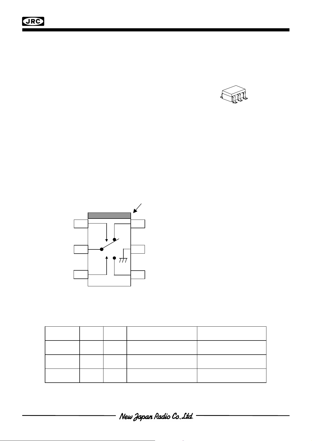
PIN CONFIGURATION
F Type
(Top View)
n
PACKAGE OUTLINE
NJG1509F
=3.0V
CTL
n
TRUTH TABLE
1
2
V
V
CTL1
CTL2
H L L H
L H L H
P1-PC OFF ON
P2-PC ON OFF
6
Pin connection
1.V
2.PC
5
3.V
4.P2
5.GND
6.P1
(H), “L”=V
“H”=V
43
CTR
Loss =15dB
P1 Return Loss =-3dB
Loss =15dB
P2 Return Loss =-3dB
CTL1
CRL2
CTR
(L)
Loss =16dB
P1 Return Loss =-2dB
Loss =16dB
P2 Return Loss =-2dB
Note) The values of “Loss” and “Return Loss” are typical values.
Page 2
NJG1509F
- 2 -
n
ABSOLUTE MAXIMUM RATINGS
PARAMETER SYMBOL RATINGS UNITS
(Ta=25°C)
Input Power P
Control Voltage V
Power Dissipation P
Operating Temp. T
Storage Temp. T
n
ELECTRICAL CHARACTERISTICS
in
CTL
D
opr
stg
31 dBm
6 V
300 mW
-30~+85 °C
-40~+150 °C
(V
CTL (L)
=0V, V
CTL(H)
=2.7V, ZS=ZO=50Ω, Ta=25°C)
PARAMETER SYMBOL CONDITIONS MIN TYP MAX UNITS
Control voltage (L) V
Control voltage (H) V
Control current I
CTL (L)
CTL (H)
CTL
f=0.05~2.5GHz, Pin=10dBm -0.2 0 0.2 V
f=0.05~2.5GHz, Pin=10dBm 2.5 2.7 5.5 V
f=0.05~2.5GHz, Pin=10dBm - 5.0 8.0 uA
Insertion loss 1 LOSS1 f=1GHz, Pin=22dBm - 0.4 0.7 dB
Insertion loss 2 LOSS2 f=2GHz, Pin=22dBm - 0.5 0.8 dB
Isolation 1
(PC-P1, PC-P2, P1-P2)
Isolation 2
(PC-P1, PC-P2, P1-P2)
ISL1 f=1GHz, Pin=22dBm 23 28 - dB
ISL2 f=2GHz, Pin=22dBm 20 25 - dB
Pin at 1dB
compression point 1
P
-1dB1
f=2GHz 26 28 - dBm
Pin at 1dB
compression point 2
P
-1dB2
V
CTL (H)
=3.0V, f=2GHz 27 30 - dBm
VSWR (PC, P1, P2) VSWR f=0.05~2.5GHz, ON State - 1.3 1.6
Switching time T
SW
f=0.05~2.5GHz - 15 - ns
Page 3
NJG1509F
- 3 -
n
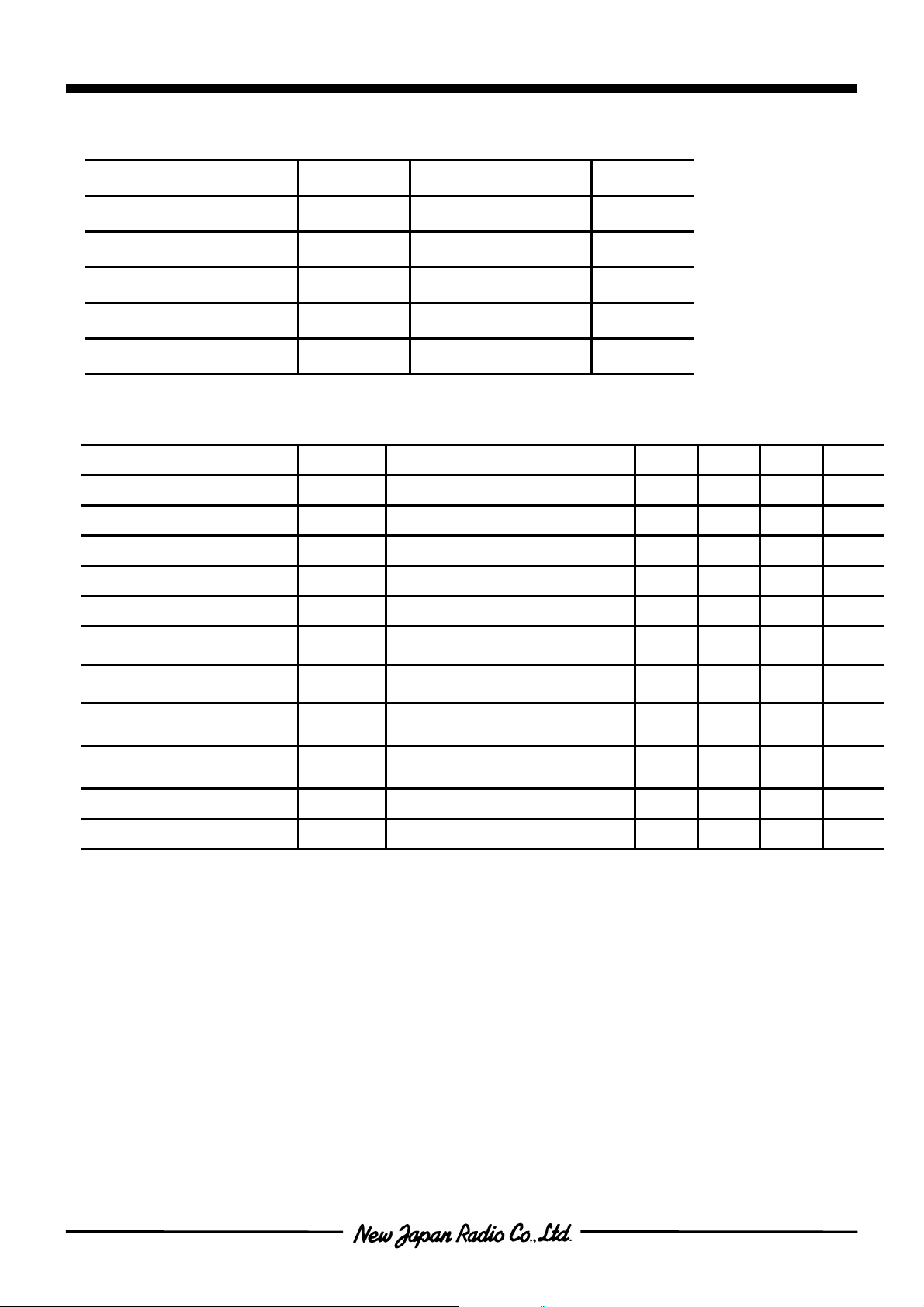
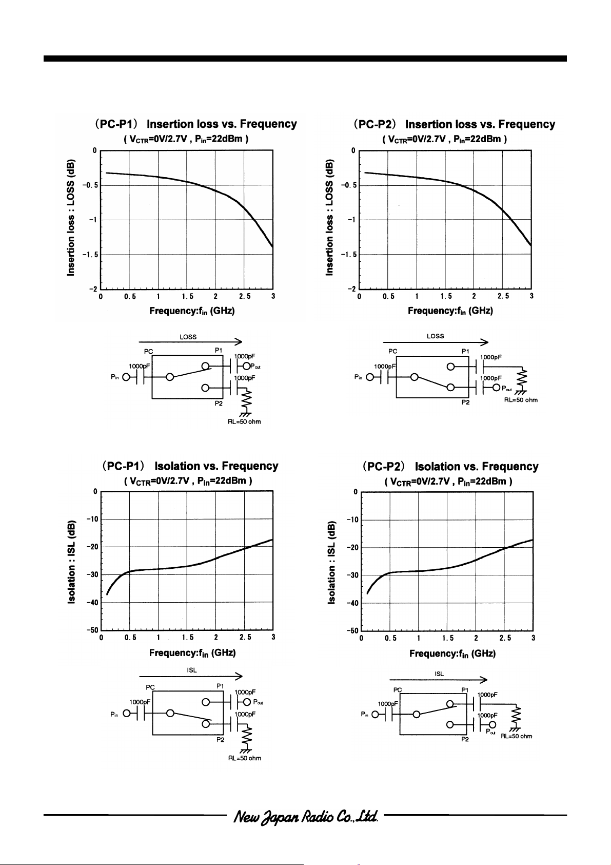
TYPICAL CHARACTERISTICS
Page 4
NJG1509F
- 4 -
n
TYPICAL CHARACTERISTICS
Page 5

NJG1509F
- 5 -
n
TYPICAL CHARACTERISTICS
Page 6

NJG1509F
- 6 -
n
TYPICAL CHARACTERISTICS
Page 7

NJG1509F
- 7 -
n
TYPICAL CHARACTERISTICS
Page 8

NJG1509F
- 8 -
n
TYPICAL CHARACTERISTICS
Page 9

NJG1509F
- 9 -
n
4 2000 0.723 68.7
TYPICAL CHARACTERISTICS
MARKER f (MHz) Mag. Ang. (
1 50 0.954 -15.4
2 800 0.755 -172.5
3 1500 0.716 113.6
4 2000 0.710 72.3
5 3000 0.693 1.4
∠
o
)
MARKER f (MHz) Mag. Ang. (
∠
1 50 0.952 -15.5
2 800 0.767 -173.6
3 1500 0.731 111.1
o
)
Page 10

NJG1509F
- 10 -
n
TYPICAL CHARACTERISTICS
Scattering Parameters: S11 (OFF STATE)
(V
=0/2.7V, 50ΩSystem)
CTR
Page 11

NJG1509F
- 11 -
n
APPLICATION CIRCUIT 1: Single control signal operation by using C-MOS inverter.
[1]Please connect bypass capacitors to the supply terminal of the C-MOS inverter.
[2]In order to stabilize input impedance of inverter, please pull down using 510KΩ
resister from the input terminal of the C-MOS inverter to the ground plane.
n
APPLICATION CIRCUIT 2: Single control signal operation by using a transistor.
Page 12

NJG1509F
- 12 -
n
TEST CIRCUIT
P2
Zo=50Ω
C2
V
(2.7V/0V)
CTR2
4
3
C4
Zo=50Ω
P1
n
RECOMMENDED PCB DESIGN
(TOP VIEW)
V
CTR2
C4
P2
C2
PC
C3
C1
R1
5
6
NJG1509F
V
C5
CTR1
C1
P1
C3
V
Zo=50Ω
CTR1
PC
(0V/2.7V)
2
R1
1
C5
PCB SIZE=19.4x14.0mm
PCB: FR-4, t=0.5mm
CAPACITOR: size 1005
STRIP LINE WIDTH=1mm
C1~C3: 56pF
Precaution
C4, C5: 10pF
R1: 510KΩ
[1]External capacitors should be connected to the input and output RF terminals (P1,
P2, PC) to block the DC current. The above example is a circuit at 900MHz. Please
select the capacitors value suitable for actual frequency from 10pF to 1000pF.
[2]Decoupling capacitors should be connected to the control terminals (V
CTR1
, V
CTR2
as close as possible. The values of these capacitors should be selected from 5pF
to 100pF range. Please consider that these values are very effective to switching
time (Larger capacitor gives longer switching time).
[3]In order to keep good isolation characteristics, the grand terminal (5pin) should be
connected to the ground pattern with wide width as close as possible, and
though-hole in the ground plane should also be placed as close as possible.
)
Page 13

NJG1509F
- 13 -
nPACKAGE OUTLINE (MTP6)
Lead material : Copper
Lead surface finish : Solder plating
Molding material : Epoxy resin
UNIT : mm
Weight : 14mg
Cautions on using this product
This product contains Gallium-Arsenide (GaAs) which is a harmful material.
• Do NOT eat or put into mouth.
• Do NOT dispose in fire or break up this product.
• Do NOT chemically make gas or powder with this product.
• To waste this product, please obey the relating law of your country.
This product may be damaged with electric static discharge (ESD) or spike voltage. Please handle with
care to avoid these damages.
[CAUTION]
The specifications on this databook are only
given for information , without any guarantee
as regards either mistakes or omissions. The
application circuits in this databook are
described only to show representative usages
of the product and not intended for the
guarantee or permission of any right including
the industrial rights.
 Loading...