

Page 1
NJG1308F
DRIVER-AMPLIFIER GaAs MMIC
NJG1308F
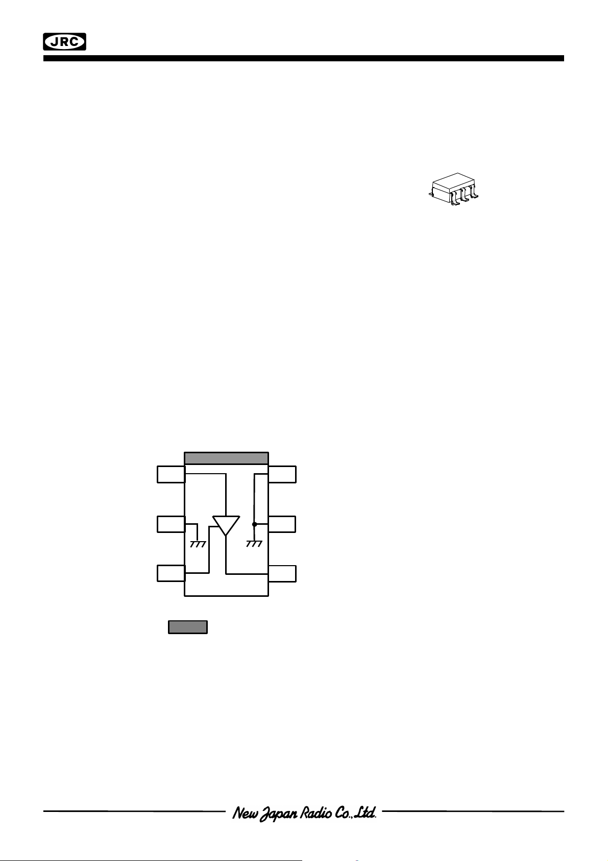
Pin connection
nGENERAL DESCRIPTION nPACKAGE OUTLINE
NJG1308F is a GaAs MMIC Driver-Amplifier for 800MHz-
1.9 GHz band of Cellular phone System.
It features a low current consumption and a high gain.
Small MTP6 package is adopted.
nFEATURES
lLow supply voltage operation +3.0V typ.
lLow current consumption 15mA typ. @P
lHigh gain 18dB typ. @f=938MHz
16dB @f=1441MHz
14dB @f=1900MHz
lPout at 1dB Gain Compression point +12dBm typ. @f=938MHz
+11dBm typ. @f=1441/1900MHz
lpackage MTP6
nPIN CONFIGURATION
=+8dBm
out
F TYPE
(Top View)
1
2
3
Note: is a package orientation mark.
6
1.RF
2.GND
5
3.BPC
4.RF
5.GND
6.GND
4
in
out
& V
DD
Page 2

NJG1308F
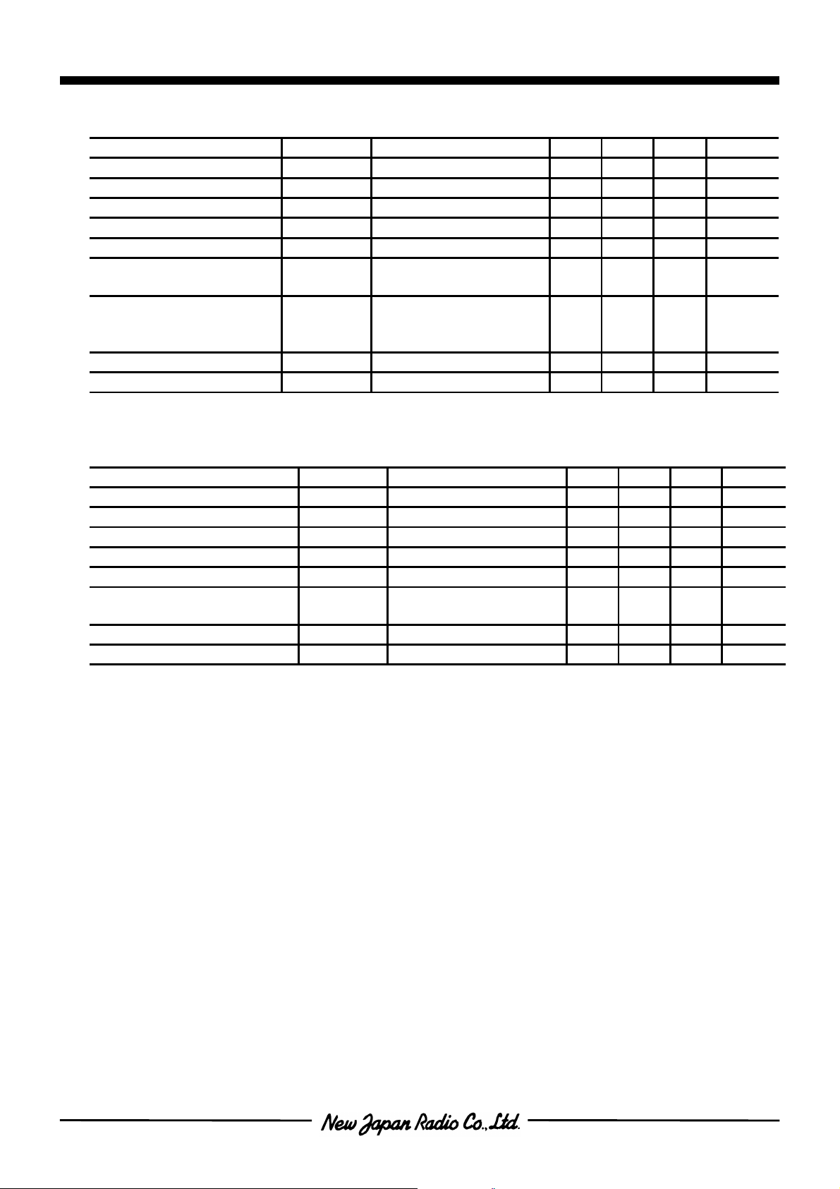
nABSOLUTE MAXIMUM RATINGS
(Ta=+25°C, Zs=Zl=50Ω)
PARAMETER SYMBOL CONDITIONS RATINGS UNITS
Drain Voltage V
Input Power P
Power Dissipation P
Operating Temperature T
Storage Temperature T
DD
opr
stg
in
D
VDD=3V 15 dBm
6 V
300 mW
-40~+85 °C
-55~+150 °C
nELECTRICAL CHARACTERISTICS 1(Application circuit 1)
(Ta=+25°C, Zs=Zl=50Ω)
PARAMETER SYMBOL CONDITIONS MIN TYP MAX UNITS
Operating Frequency Freq VDD=3.0V 915 938 960 MHz
Drain Voltage V
Operating Current I
DD
DD
VDD=3.0V, P
=+8dBm - 15 21 mA
out
2.7 3.0 5.0 V
Small Signal Gain Gain VDD=3.0V, Pin=-10dBm 15 18 21 dB
Gain Flatness G
Pout at 1dB Gain
Compression point
flat
P
-1dB
Adjacent Channel
Leakage Power
P
acp
(PDC Regulation)
Input VSWR VSWR
Output VSWR VSWR
VDD=3.0V, Pin=-10dBm - 0.5 - dB
VDD=3.0V - +12 - dBm
VDD=3.0V, P
offset=50kHz
=+8dBm
out
- -60 - dBc
Pin;π/4 DQPSK
VDD=3.0V - 1.5 -
i
VDD=3.0V - 1.5 -
o
nELECTRICAL CHARACTERISTICS 2 (Application circuit 2)
(Ta=+25°C, Zs=Zl=50Ω)
PARAMETER SYMBOL CONDITIONS MIN TYP MAX UNITS
Operating Frequency freq VDD=3.0V 1429 1441 1453 MHz
Drain Voltage V
Operating Current I
DD
DD
VDD=3.0V, P
=+8dBm - 15 21 mA
out
2.7 3.0 5.0 V
Small Signal Gain Gain VDD=3.0V, Pin=-10dBm 13 16 19 dB
Gain Flatness G
Pout at 1dB Gain
Compression point
flat
P
-1dB
Adjacent Channel
Leakage Power
P
acp
(PDC Regulation)
Input VSWR VSWR
Output VSWR VSWR
VDD=3.0V, Pin=-10dBm - 0.5 - dB
VDD=3.0V - +11 - dBm
VDD=3.0V, P
offset=50kHz
=+8dBm
out
- -60 - dBc
Pin; π/4 DQPSK
VDD=3.0V - 1.5 -
i
VDD=3.0V - 1.5 -
o
Page 3
NJG1308F
nELECTRICAL CHARACTERISTICS 3 (Application circuit 3)
(Ta=+25°C, Zs=Zl=50Ω)
PARAMETER SYMBOL CONDITIONS MIN TYP MAX UNITS
Operating Frequency freq VDD=3.0V 1890 1900 1920 MHz
Drain Voltage V
Operating Current I
DD
DD
VDD=3.0V, P
=+8dBm - 15 21 mA
out
2.7 3.0 5.0 V
Small Signal Gain Gain VDD=3.0V, Pin=-10dBm 11 14 17 dB
Gain Flatness G
Pout at 1dB Gain
Compression point
flat
P
-1dB
Adjacent Channel
Leakage Power
P
acp
(PHS Regulation)
Input VSWR VSWR
Output VSWR VSWR
VDD=3.0V, Pin=-10dBm - 0.5 - dB
VDD=3.0V - +11 - dBm
VDD=3.0V, P
offset=600kHz
=+8dBm
out
- -60 - dBc
Pin; π/4 DQPSK
VDD=3.0V - 1.5 -
i
VDD=3.0V - 1.5 -
o
nELECTRICAL CHARACTERISTICS 4 (Application Circuit 4)
(Ta=+25°C, Zs=Zl=50Ω)
PARAMETER SYMBOL CONDITIONS MIN TYP MAX UNITS
Operating Frequency freq VDD=3.0V 1750 1765 1780 MHz
Supply Voltage V
Operating Current I
DD
DD
VDD=3.0V, P
=+8dBm - 15 - mA
out
2.7 3.0 5.0 V
Power Gain Gain VDD=3.0V, Pin=-10dBm - 14 - dB
Gain Flatness G
Pout at 1dB
Compression point
flat
P
-1Db
Input VSWR VSWR
Output VSWR VSWR
VDD=3.0V, Pin=-10dBm - 0.5 - dB
VDD=3.0V - +11 - dBm
VDD=3.0V - 1.5 -
I
VDD=3.0V - 1.5 -
o
Page 4

NJG1308F
nTYPICAL CHARACTERISTICS 1 (Application Circuit 1)
Page 5

NJG1308F
nTYPICAL CHARACTERISTICS 2 (Application Circuit 2)
Page 6

NJG1308F
nTYPICAL CHARACTERISTICS 3 (Application Circuit 3)
Page 7

NJG1308F
nTYPICAL CHARACTERISTICS 4 (Application Circuit 4)
S21,S11,S22,S12 vs. FREQUENCY
20
S21
(VDD=3V)
-10
10
0
-10
S21,S11,S22 (dB)
-20
-30
0.5 1 1.5 2 2.5 3
S12
S22
S11
Frequency (GHz)
-20
-30
-40
-50
-60
S12 (dB)
Page 8

NJG1308F
nTYPICAL CHARACTERISTICS
Freq.
S11S21S12S22mag
ang
mag
ang
mag
ang
mag
ang
(GHz)
(U)
(deg)
(U)
(deg)
(U)
(deg)
(U)
(deg)
0.50
0.865
-26.1
4.892
174.0
0.029
52.0
0.718
-56.5
0.60
0.853
-32.2
5.060
163.2
0.030
48.7
0.681
-63.4
0.70
0.834
-38.2
5.093
152.9
0.033
46.2
0.648
-69.6
0.80
0.810
-43.7
5.046
143.5
0.035
46.4
0.626
-74.9
0.90
0.788
-48.5
4.974
134.5
0.036
44.5
0.603
-78.8
1.00
0.757
-52.8
4.801
126.4
0.038
43.5
0.590
-82.4
1.10
0.729
-56.7
4.650
118.6
0.039
42.7
0.580
-85.6
1.20
0.700
-60.3
4.457
111.5
0.041
44.0
0.579
-88.8
1.30
0.672
-63.1
4.271
104.6
0.043
43.3
0.577
-90.9
1.40
0.645
-65.6
4.083
98.0
0.045
44.6
0.581
-93.6
1.50
0.618
-67.7
3.893
91.3
0.046
44.0
0.588
-96.0
1.60
0.589
-69.0
3.687
85.2
0.049
43.8
0.597
-98.5
1.70
0.563
-69.7
3.509
79.3
0.051
42.4
0.612
-100.8
1.80
0.541
-69.8
3.317
72.9
0.055
40.3
0.630
-103.7
1.90
0.519
-69.6
3.122
66.5
0.058
38.3
0.650
-106.9
2.00
0.502
-67.9
2.904
60.0
0.060
35.8
0.671
-110.2
2.10
0.489
-65.9
2.696
53.6
0.063
31.4
0.700
-114.5
2.20
0.490
-62.3
2.432
46.6
0.065
25.7
0.728
-119.5
2.30
0.502
-58.9
2.150
39.1
0.065
17.4
0.764
-125.8
2.40
0.536
-55.6
1.814
31.9
0.066
8.5
0.795
-132.8
2.50
0.592
-53.5
1.409
24.6
0.062
-5.9
0.828
-142.1
2.60
0.669
-53.8
0.933
21.3
0.056
-24.0
0.846
-153.2
2.70
0.760
-56.9
0.461
41.1
0.050
-54.3
0.842
-166.5
2.80
0.851
-62.8
0.575
106.1
0.048
-96.7
0.800
178.6
2.90
0.920
-70.6
1.154
113.3
0.060
-140.4
0.731
161.6
3.00
0.951
-79.2
1.703
105.2
0.081
-172.8
0.624
144.2
Ω
Ω
Ω
Ω
Scattering Parameters (VDD=3V)
nPIN CONNECTIONS AND FUNCTIONAL BLOCK DIAGRAM
RF IN
ZO=50
ZS=50
V
DD
RF OUT
4
AMP1
3
6
5
2
ZO=50
ZL=50
Page 9

NJG1308F
nAPPLICATION CIRCUIT1
nAPPLICATION CIRCUIT 2
Page 10

NJG1308F
nAPPLICATION CIRCUIT 3
nAPPLICATION CIRCUIT 4
Page 11

NJG1308F
nRECOMMENDED PCB DESIGN
VDD
NJG
1308F
GND
C1
RFin
PCB:FR-4 22.5x20.0mm, t=0.5mm
MICROSTRIP LINE WIDTH=1.0mm (Zo=50Ω)
CHIP SIZE:1608
L1
C2
R1
C3
GND
C4
L2
L3
RFout
C6
C5
Notes:
[1] Following chip capacitor should be connected near to each terminal as bypass capacitor.
(1) C3
(2) C4
[2] Following chip capacitors are necessary to block DC bias.
(3) C1
(4) C6
[3] Chip parts list.
Parts ID Comment
C1~C6 MURATA GRM39 Series
L1~L3 TAIYO-YUDEN HK1608 Series
Page 12

NJG1308F
nPACKAGE OUTLINE (MTP6)
• To waste this product, please obey the relating law of your country.
with care to avoid these damages .
[CAUTION]
Lead material : Copper
Lead surface finish : Solder plating
Molding material : Epoxy resin
UNIT : mm
Weight : 14mg
Cautions on using this product
This product contains Gallium-Arsenide (GaAs) which is a harmful material.
• Do NOT eat or put into mouth.
• Do NOT dispose in fire or break up this product.
• Do NOT chemically make gas or powder with this product.
This product may be damaged with electric static discharge (ESD) or spike voltage. Please handle
The specifications on this databook are only
given for information , without any guarantee
as regards either mistakes or omissions. The
application circuits in this databook are
described only to show representative usages
of the product and not intended for the
guarantee or permission of any right including
the industrial rights.
 Loading...