

Page 1
NJG1107KB2
1.5/1.9GHz LNA GaAs MMIC
PIN Connection
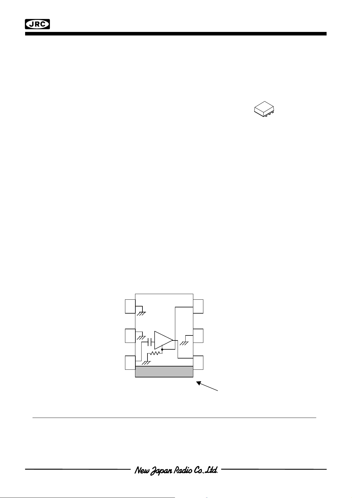
nGENERAL DESCRIPTION nPACKAGE OUTLINE
NJG1107KB2 is a Low Noise Amplifier GaAs MMIC
designed for 1.5GHz and 1.9GHz band digital cellular phone
and Japanese PHS handsets. This amplifier provides low
noise figure, high gain and high IP3 operated by single low
positive power supply.
This amplifier includes internal self-bias circuit and input
DC blocking capacitor.
An ultra small and thin package of FLP6 is adopted.
nFEATURES
lLow voltage operation +2.7V typ.
lLow current consumption 3.0mA typ.
lHigh small signal gain 17dB typ. @f=1.49GHz
15dB typ. @f=1.96GHz
lLow noise figure 1.2dB typ. @f=1.49GHz
1.2dB typ. @f=1.96GHz
lHigh Input IP3 -4.0dBm typ. @f=1.4900+1.4901GHz
-2.0dBm typ. @f=1.9600+1.9601GHz
lUltra small & ultra thin package FLP6-B2 (Mount Size: 2.1x2.0x0.75mm)
NJG1107KB2
l This amplifier can be tuned into various frequency range.(Best for 1.5GHz or 1.9GHz Band)
nPIN CONFIGURATION
KB2 Type
(Top View)
4
5
6
AMP
3
1.RFout
2.GND
2
1
3.EXTCAP
4.GND
5.GND
6.RFin
Orientation Mark
Note: Specifications and description listed in this catalog are subject to change without prior notice.
- 1 -
Page 2
NJG1107KB2
nABSOLUTE MAXIMUM RATINGS
(Ta=+25°C, Zs=Zl=50Ω)
PARAMETER SYMBOL CONDITIONS RATINGS UNIT
Drain Voltage V
DD
6.0 V
Input Power Pin VDD=2.7V +15 dBm
Power Dissipation P
Operating Temp. T
Storage Temp. T
D
opr
stg
450 mW
-40~+85 °C
-55~+125 °C
nELECTRICAL CHARACTERISTICS 1 (1.5GHz Band)
(VDD=2.7V, f=1.49GHz, Ta=+25°C, Zs=Zl=50Ω, TEST CIRCUIT1)
PARAMETER SYMBOL CONDITIONS MIN TYP MAX UNIT
Operating Frequency freq1 1.47 1.49 1.51 GHz
Drain Voltage V
Operating Current I
DD
DD
RF OFF - 3.0 3.8 mA
2.5 2.7 5.5 V
Small Signal Gain Gain 15.0 17.0 19.0 dB
Gain Flatness G
flat
f=1.47~1.51GHz - 0.5 1.0 dB
Noise Figure NF - 1.2 1.4 dB
Pout at 1dB Gain
Compression point
Input 3rd Order
Intercept Point
RF Input Port
VSWR
RF Output Port
VSWR
P
-1dB
IIP3
VSWR
VSWR
f=1.49+1.4901GHz
RFin=-35dBm
i
o
-6.0 -2.0 - dBm
-6.0 -4.0 - dBm
- 1.6 2.2
1.6 2.2
nELECTRICAL CHARACTERISTICS 2 (1.9GHz Band)
(VDD=2.7V, f=1.96GHz, Ta=+25°C, Zs=Zl=50Ω, TEST CIRCUIT1)
PARAMETER SYMBOL CONDITIONS MIN TYP MAX UNIT
Operating Frequency freq2 1.89 1.96 1.99 GHz
Drain Voltage V
Operating Current I
DD
DD
RF OFF - 3.0 3.8 mA
2.5 2.7 5.5 V
Small Signal Gain Gain 13.0 15.0 17.0 dB
Gain Flatness G
flat
f=1.89~1.99GHz - 0.5 1.0 dB
Noise Figure NF - 1.2 1.4 dB
Pout at 1dB Gain
Compression point
Input 3rd order
Intercept Point
RF Input Port
VSWR
RF Output Port
VSWR
P
-1dB
IIP3
VSWR
VSWR
f=1.96+1.9601GHz
RFin=-30dBm
i
o
-3.0 +1.0 - dBm
-6.0 -2.0 - dBm
- 1.6 2.2
- 1.6 2.2
- 2 -
Page 3
NJG1107KB2
nELECTRICAL CHARACTERISTICS 3 (1.8GHz Band)
(VDD=2.7V, f=1.76GHz, Ta=+25°C, Zs=Zl=50Ω, TEST CIRCUIT1)
PARAMETER SYMBOL CONDITIONS MIN TYP MAX UNIT
Operating Frequency freq3 1.75 1.76 1.78 GHz
Drain Voltage V
Operating Current I
DD
DD
RF OFF - 3.0 3.8 mA
2.5 2.7 5.5 V
Small Signal Gain Gain - 16.0 - dB
Gain Flatness G
flat
f=1.75~1.78GHz - 0.5 - dB
Noise Figure NF - 1.2 - dB
Pout at 1dB
Compression point
Input 3rd order
Intercept Point
RF Input Port
VSWR
RF Output Port
VSWR
P
-1dB
IIP3
VSWR
VSWR
f=1.76+1.7601GHz
RFin=-35dBm
i
o
- 1.1 - dBm
- -2.0 - dBm
- 1.6 - -
- 1.6 - -
nELECTRICAL CHARACTERISTICS 4 (1.5GHz Band ,Low Gain Version)
(VDD=2.7V, f=1.49GHz, Ta=+25°C, Zs=Zl=50Ω, TEST CIRCUIT2)
PARAMETER SYMBOL CONDITIONS MIN TYP MAX UNIT
Operating Frequency freq4 1.47 1.49 1.51 GHz
Drain Voltage V
Operating Current I
DD
DD
RF OFF - 3.0 3.8 mA
2.5 2.7 5.5 V
Small Signal Gain Gain - 14.0 - dB
Gain Flatness G
flat
f=1.47~1.51GHz - 0.5 - dB
Noise Figure NF - 1.2 - dB
Pout at 1dB
Compression point
Input 3rd order
Intercept Point
RF Input Port
VSWR
RF Output Port
VSWR
P
-1dB
IIP3
VSWR
VSWR
f=1.49+1.4901GHz
RFin=-35dBm
i
o
- 0.0 - dBm
- -3.0 - dBm
- 1.6 -
- 1.6 -
- 3 -
Page 4
NJG1107KB2
nPIN CONFIGURATION
Pin Function Description
RF output and voltage supply pin. External matching circuits and a bypass capacitor
1 RFout
2,4,5 GND
3 EXTCAP An external bypass capacitor is required. (Please refer to “TEST CIRCUIT”)
6 RFin
is required. L3 is a RF choke inductor and C1 is a DC blocking capacitor. These
elements are used as output matching circuit. C2 is a bypass capacitor. (Please refer
to “TEST CIRCUIT”)
Ground pin. To keep good RF grounding performance, please use multiple via holes
to connect with ground plane and this pin.
RF input pin. A DC blocking capacitor is not required. An external matching circuit is
required. (Please refer to “TEST CIRCUIT”)
- 4 -
Page 5
NJG1107KB2
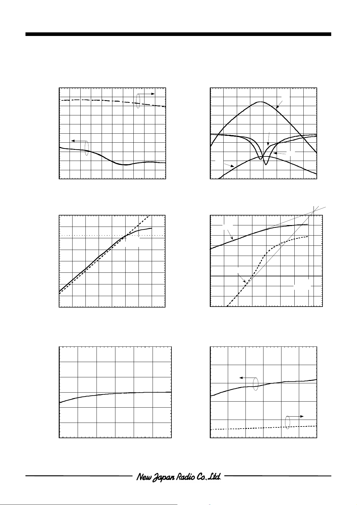
nTYPICAL CHARACTERISTICS (1.5GHz Band)
NF,Gain vs. frequency
2.6
2.2
1.8
NF (dB)
1.4
1
0.6
1.4 1.44 1.48 1.52 1.56 1.6
frequency (GHz)
(VDD=2.7V,IDD=3mA)
Pout vs. Pin
(VDD=2.7V,f=1.49GHz)
10
0
-10
Pout (dBm)
-20
P-1dB
+1.17dBm
20
16
12
8
4
0
10
5
0
-5
-10
-15
-20
-25
Gain (dB)
S21,S11,S22,S12 vs. frequency
25
20
15
10
5
0
-5
S21,S11,S22 (dB)
-10
-15
S12
-20
-25
0.5 1 1.5 2 2.5
frequency (GHz)
(VDD=2.7V,IDD=3mA)
S21
S11
S22
Pout, IM3 vs. Pin
(VDD=2.7V,IDD=3mA,f=1.49+1.4901GHz)
10
0
Pout
-10
-20
-30
-40
Pout,IM3 (dBm)
-50
-60
-70
IM3
IIP3
-3.15dBm
50
40
30
20
10
0
-10
-20
-30
-40
-50
S12 (dB)
-30
-40 -30 -20 -10 0
19
18.5
18
17.5
Gain (dB)
17
16.5
16
2.5 3 3.5 4 4.5 5 5.5
Pin (dBm)
Gain vs. V
VDD (V)
DD
(f=1.49GHz)
-30
-80
-40 -30 -20 -10 0
Pin (dBm)
NF, IDD vs. V
1.3
1.2
1.1
NF (dB)
1
0.9
0.8
2.5 3 3.5 4 4.5 5 5.5
VDD (V)
DD
(f=1.49GHz)
3.4
3.3
3.2
3.1
3
2.9
(mA)
DD
I
- 5 -
Page 6
NJG1107KB2
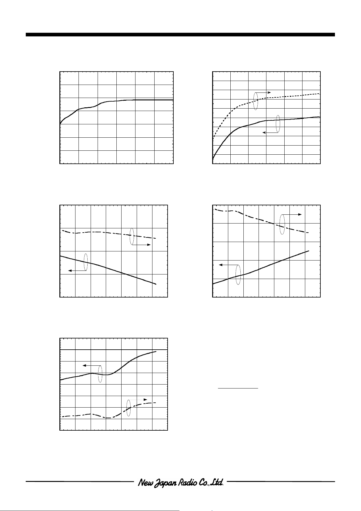
nTYPICAL CHARACTERISTICS (1.5GHz Band)
Equations of OIP3 and IIP3
P-1dB vs. V
8
6
4
2
0
P-1dB (dBm)
-2
-4
-6
2.5 3 3.5 4 4.5 5 5.5
VDD (V)
DD
(f=1.49GHz)
Gain, IDD vs. Temperature
20
19
(VDD=2.7V, f=1.49GHz)
3.25
3
IIP3, OIP3 vs. V
5
4
3
2
1
0
-1
IIP3 (dBm)
-2
-3
-4
-5
2.5 3 3.5 4 4.5 5 5.5
(f=1.49+1.4901GHz, Pin=-35dBm)
DD
VDD (V)
NF, P-1dB vs. Temperature
2.4
2
(VDD=2.7V, f=1.49GHz)
20
19
18
17
16
15
14
13
12
11
10
2
1
OIP3 (dBm)
18
Gain (dB)
17
16
-40 -20 0 20 40 60 80 100
Temperature ( )
o
C
IIP3, OIP3 vs. Temperature
0
-1
-2
-3
-4
IIP3 (dBm)
-5
-6
(VDD=2.7V, f=1.49+1.4901GHz, Pin=-35dBm)
2.75
2.5
2.25
21
20
19
18
17
16
15
(mA)
DD
I
NF (dB)
OIP3 (dBm)
1.6
1.2
0.8
0.4
-40 -20 0 20 40 60 80 100
Temperature ( )
=3OIP
3IM-Pout×3
2
Gain-3OIP=3IIP
o
C
@ Pin=-35dBm
0
-1
-2
-3
P-1dB (dBm)
-7
-8
-40 -20 0 20 40 60 80 100
- 6 -
Temperature ( )
o
14
13
C
Page 7

NJG1107KB2
nTYPICAL CHARACTERISTICS (1.5GHz Band)
S11 vs. frequency ( to 20GHz)
25
20
15
10
5
0
S11 (dB)
-5
-10
-15
-20
-25
0 2 4 6 8 10 12 14 16 18 20
frequency (GHz)
(VDD=2.7V,IDD=3mA)
S21 vs. frequency ( to 20GHz)
25
20
15
10
5
0
S21 (dB)
-5
-10
-15
-20
-25
0 2 4 6 8 10 12 14 16 18 20
frequency (GHz)
(VDD=2.7V,IDD=3mA)
S22 vs. frequency ( to 20GHz)
25
20
15
10
5
0
S22 (dB)
-5
-10
-15
-20
-25
0 2 4 6 8 10 12 14 16 18 20
frequency (GHz)
(VDD=2.7V,IDD=3mA)
S12 vs. frequency ( to 20GHz)
25
20
15
10
5
0
S12 (dB)
-5
-10
-15
-20
-25
0 2 4 6 8 10 12 14 16 18 20
frequency (GHz)
(VDD=2.7V,IDD=3mA)
- 7 -
Page 8

NJG1107KB2
nTYPICAL CHARACTERISTICS (1.9GHz Band)
NF,Gain vs. frequency
2.6
2.2
1.8
NF (dB)
1.4
1
0.6
1.8 1.84 1.88 1.92 1.96 2
frequency (GHz)
(VDD=2.7V,IDD=3mA)
20
16
12
8
4
0
Gain (dB)
S21,S11,S22,S12 vs. frequency
25
20
15
10
5
0
-5
S21,S11,S22 (dB)
-10
-15
-20
-25
1 1.5 2 2.5 3
S12
frequency (GHz)
(VDD=2.7V,IDD=3mA)
S21
S22
S11
50
40
30
20
10
0
-10
-20
-30
-40
-50
S12 (dB)
Pout vs. Pin
(VDD=2.7V,f=1.96GHz)
10
0
-10
Pout (dBm)
-20
-30
-40 -30 -20 -10 0
Pin (dBm)
Gain vs. V
17
16.5
16
15.5
Gain (dB)
15
P-1dB
+1.17dBm
DD
(f=1.96GHz)
Pout, IM3 vs. Pin
(VDD=2.7V,IDD=3mA,f=1.96+1.9601GHz)
10
0
Pout
-10
-20
-30
-40
-50
Pout,IM3 (dBm)
-60
-70
-80
-90
-40 -30 -20 -10 0
1.3
1.2
1.1
NF (dB)
1
IM3
Pin (dBm)
NF, IDD vs. V
DD
-2.21dBm
(f=1.96GHz)
IIP3
3.4
3.3
3.2
3.1
(mA)
DD
I
14.5
14
2.5 3 3.5 4 4.5 5 5.5
- 8 -
VDD (V)
0.9
0.8
2.5 3 3.5 4 4.5 5 5.5
VDD (V)
3
2.9
Page 9

NJG1107KB2
nTYPICAL CHARACTERISTICS (1.9GHz Band)
P-1dB vs. V
8
6
4
2
0
P-1dB (dBm)
-2
-4
-6
2.5 3 3.5 4 4.5 5 5.5
Gain, IDD vs. Temperature
18
DD
(f=1.96GHz)
VDD (V)
(VDD=2.7V, f=1.96GHz)
3.25
IIP3, OIP3 vs. V
6
5
4
3
2
1
0
IIP3 (dBm)
-1
-2
-3
-4
2.5 3 3.5 4 4.5 5 5.5
(f=1.96+1.9601GHz, Pin=-30dBm)
DD
VDD (V)
NF, P-1dB vs. Temperature
2.4
(VDD=2.7V, f=1.96GHz)
20
19
18
17
16
15
14
13
12
11
10
2
OIP3 (dBm)
17
16
Gain (dB)
15
14
-40 -20 0 20 40 60 80 100
Temperature ( )
o
C
IIP3, OIP3 vs. Temperature
1
0
-1
-2
-3
IIP3 (dBm)
-4
-5
-6
-7
-40 -20 0 20 40 60 80 100
(VDD=2.7V, f=1.96+1.9601GHz, Pin=-30dBm)
Temperature ( )
o
C
3
2.75
2.5
2.25
20
19
18
17
16
15
14
13
12
(mA)
DD
I
OIP3 (dBm)
2
1.6
NF (dB)
1.2
0.8
0.4
-40 -20 0 20 40 60 80 100
Temperature ( )
o
C
Equations of OIP3 and IIP3
=3OIP
Gain-3OIP=3IIP
3IM-Pout×3
2
@ Pin=-30dBm
1
0
-1
-2
-3
P-1dB (dB)
- 9 -
Page 10

NJG1107KB2
nTYPICAL CHARACTERISTICS (1.9GHz Band)
S11 vs. frequency ( to 20GHz)
25
20
15
10
5
0
S11 (dB)
-5
-10
-15
-20
-25
0 2 4 6 8 10 12 14 16 18 20
frequency (GHz)
(VDD=2.7V,IDD=3mA)
S21 vs. frequency ( to 20GHz)
25
20
15
10
5
0
S21 (dB)
-5
-10
-15
-20
-25
0 2 4 6 8 10 12 14 16 18 20
frequency (GHz)
(VDD=2.7V,IDD=3mA)
S22 vs. frequency ( to 20GHz)
25
20
15
10
5
0
S22 (dB)
-5
-10
-15
-20
-25
0 2 4 6 8 10 12 14 16 18 20
frequency (GHz)
(VDD=2.7V,IDD=3mA)
S12 vs. frequency ( to 20GHz)
25
20
15
10
5
0
S12 (dB)
-5
-10
-15
-20
-25
0 2 4 6 8 10 12 14 16 18 20
frequency (GHz)
(VDD=2.7V,IDD=3mA)
- 10 -
Page 11

NJG1107KB2
nTYPICAL CHARACTERISTICS (1.8GHz Band)
NF,Gain vs. frequency
(VDD=2.7V,IDD=3mA)
2.6
2.2
1.8
NF (dB)
1.4
1
0.6
1.65 1.7 1.75 1.8 1.85
frequency (GHz)
20
16
12
8
4
0
Gain (dB)
S21,S11,S22,S12 vs. frequency
25
20
15
10
5
0
-5
S21,S11,S22 (dB)
-10
-15
-20
-25
1 1.5 2 2.5 3
S12
frequency (GHz)
(VDD=2.7V,IDD=3mA)
S21
S22
S11
50
40
30
20
10
0
-10
-20
-30
-40
-50
S12 (dB)
Pout vs. Pin
(VDD=2.7V,f=1.76GHz)
10
0
-10
Pout (dBm)
-20
-30
-40 -30 -20 -10 0
Pin (dBm)
P-1dB
+1.14dBm
Pout, IM3 vs. Pin
(VDD=2.7V,IDD=3mA,f=1.76+1.7601GHz)
10
0
Pout
-10
-20
-30
-40
-50
Pout,IM3 (dBm)
-60
-70
-80
-90
-40 -30 -20 -10 0
IM3
-2.01dBm
Pin (dBm)
IIP3
- 11 -
Page 12

NJG1107KB2
nTYPICAL CHARACTERISTICS (1.8GHz Band)
S11 vs. frequency ( to 20GHz)
25
20
15
10
5
0
S11 (dB)
-5
-10
-15
-20
-25
0 2 4 6 8 10 12 14 16 18 20
frequency (GHz)
(VDD=2.7V,IDD=3mA)
S21 vs. frequency ( to 20GHz)
25
20
15
10
5
0
S21 (dB)
-5
-10
-15
-20
-25
0 2 4 6 8 10 12 14 16 18 20
frequency (GHz)
(VDD=2.7V,IDD=3mA)
50
40
30
20
10
0
-10
-20
-30
-40
-50
S22 vs. frequency ( to 20GHz)
25
20
15
10
5
0
S22 (dB)
-5
-10
-15
-20
-25
0 2 4 6 8 10 12 14 16 18 20
frequency (GHz)
(VDD=2.7V,IDD=3mA)
S12 vs. frequency ( to 20GHz)
25
20
15
10
5
0
S12 (dB)
-5
-10
-15
-20
-25
0 2 4 6 8 10 12 14 16 18 20
frequency (GHz)
(VDD=2.7V,IDD=3mA)
50
40
30
20
10
0
-10
-20
-30
-40
-50
- 12 -
Page 13

NJG1107KB2
nTYPICAL CHARACTERISTICS (1.5GHz Band, Low Gain Version)
NF,Gain vs. frequency
2.6
2.2
1.8
NF (dB)
1.4
1
0.6
1.4 1.44 1.48 1.52 1.56 1.6
frequency (GHz)
(VDD=2.7V,IDD=3mA)
Pout vs. Pin
(VDD=2.7V,f=1.49GHz)
10
5
0
-5
-10
Pout (dBm)
-15
-20
-25
-30
-40 -35 -30 -25 -20 -15 -10 -5 0
Pin (dBm)
P-1dB
+0.00dBm
20
16
12
8
4
0
S21,S11,S22,S12 vs. frequency
25
20
15
10
5
0
Gain (dB)
-5
S21,S11,S22 (dB)
-10
-15
-20
-25
0.5 1 1.5 2 2.5
S11
S12
frequency (GHz)
(VDD=2.7V,IDD=3mA)
S21
S22
Pout, IM3 vs. Pin
(VDD=2.7V,IDD=3mA,f=1.49+1.4901GHz)
10
0
-10
-20
-30
-40
Pout,IM3 (dBm)
-50
-60
-70
-80
-40 -35 -30 -25 -20 -15 -10 -5 0
Pout
IM3
Pin (dBm)
IIP3
-2.89dBm
50
40
30
20
10
0
-10
-20
-30
-40
-50
S12 (dB)
- 13 -
Page 14

NJG1107KB2
nTYPICAL CHARACTERISTICS (1.5GHz Band, Low Gain Version)
S11 vs. frequency ( to 20GHz)
25
20
15
10
5
0
S11 (dB)
-5
-10
-15
-20
-25
0 2 4 6 8 10 12 14 16 18 20
frequency (GHz)
(VDD=2.7V,IDD=3mA)
S21 vs. frequency ( to 20GHz)
25
20
15
10
5
0
S21 (dB)
-5
-10
-15
-20
-25
0 2 4 6 8 10 12 14 16 18 20
frequency (GHz)
(VDD=2.7V,IDD=3mA)
S22 vs. frequency ( to 20GHz)
25
20
15
10
5
0
S22 (dB)
-5
-10
-15
-20
-25
0 2 4 6 8 10 12 14 16 18 20
frequency (GHz)
(VDD=2.7V,IDD=3mA)
S12 vs. frequency ( to 20GHz)
25
20
15
10
5
0
S12 (dB)
-5
-10
-15
-20
-25
0 2 4 6 8 10 12 14 16 18 20
frequency (GHz)
(VDD=2.7V,IDD=3mA)
- 14 -
Page 15

NJG1107KB2
nTYPICAL CHARACTERISTICS
Scattering Parameter Table
VDD=2.7V, IDD=3mA, Zo=50Ω
Freq
(GHz)
(units)
S11 S21 S12 S22
mag
ang
(deg)
0.1 1.000 -3.130 2.094 176.987 0.012 -25.995 0.965 -1.855
0.2 0.986 -4.217 2.074 171.002 0.002 110.707 0.967 -1.782
0.3 0.986 -6.161 2.046 165.318 0.007 92.945 0.962 -3.088
0.4 0.972 -8.026 2.012 159.545 0.003 62.606 0.960 -3.801
0.5 0.965 -10.209 1.991 153.712 0.005 103.324 0.961 -5.113
0.6 0.957 -12.032 1.943 147.933 0.004 96.002 0.953 -6.159
0.7 0.943 -13.490 1.909 143.180 0.005 75.842 0.949 -7.623
0.8 0.929 -15.249 1.851 138.232 0.008 90.203 0.940 -9.144
0.9 0.910 -16.014 1.793 133.807 0.006 93.660 0.931 -9.943
1.0 0.903 -16.960 1.765 129.856 0.009 85.810 0.928 -10.876
1.1 0.894 -18.131 1.710 125.443 0.009 95.094 0.931 -12.170
1.2 0.879 -18.645 1.673 121.935 0.010 92.781 0.921 -13.089
1.3 0.864 -19.500 1.636 118.442 0.011 91.381 0.919 -14.156
1.4 0.852 -21.338 1.627 114.415 0.012 100.617 0.919 -14.843
1.5 0.843 -22.810 1.578 110.659 0.014 99.522 0.918 -16.259
1.6 0.826 -24.483 1.541 107.013 0.014 99.175 0.914 -17.088
1.7 0.818 -24.447 1.513 104.077 0.015 100.001 0.918 -18.228
1.8 0.810 -26.509 1.503 100.734 0.016 103.271 0.925 -19.508
1.9 0.801 -27.539 1.489 97.286 0.018 106.687 0.920 -20.507
2.0 0.794 -29.642 1.452 93.725 0.019 108.548 0.921 -21.024
2.1 0.783 -30.807 1.453 90.359 0.020 106.305 0.924 -22.491
2.2 0.782 -33.473 1.421 86.597 0.022 107.071 0.922 -24.160
2.3 0.770 -34.972 1.426 83.223 0.022 107.349 0.920 -25.779
2.4 0.772 -35.870 1.391 79.970 0.026 109.866 0.919 -27.462
2.5 0.760 -37.091 1.397 76.578 0.027 112.983 0.914 -29.724
2.6 0.761 -38.975 1.376 73.069 0.030 109.600 0.920 -32.086
2.7 0.757 -40.916 1.359 68.921 0.031 106.376 0.907 -35.211
2.8 0.756 -41.260 1.322 65.450 0.034 109.318 0.902 -38.255
2.9 0.757 -42.651 1.294 62.030 0.035 106.983 0.893 -41.787
3.0 0.752 -42.892 1.267 58.521 0.036 108.989 0.879 -45.326
mag
(units)
ang
(deg)
mag
(units)
ang
(deg)
mag
(units)
ang
(deg)
4 3
5
S11 S22
6
Ref.
2
1
Ref.
Scattering Parameter
Measurement Circuit
1000pF
- 15 -
Page 16

NJG1107KB2
nTYPICAL CHARACTERISTICS (1.5GHz Band, Low Gain Version)
Scattering Parameter Table
VDD=2.7V, IDD=3mA, Zo=50Ω
mag
(units)
S11 S21 S12 S22
ang
(deg)
mag
(units)
ang
(deg)
mag
(units)
Freq
(GHz)
0.1 1.011 -1.815 0.619 -137.421 0.006 150.071 0.998 -1.269
0.2 1.023 -4.177 1.049 -141.929 0.005 111.664 0.996 -3.638
0.3 1.027 -6.876 1.402 -152.156 0.004 72.732 0.999 -4.808
0.4 1.036 -10.171 1.681 -164.509 0.008 71.899 0.995 -6.754
0.5 1.029 -13.604 1.843 -176.486 0.006 80.582 0.993 -8.514
0.6 1.027 -17.041 1.967 172.550 0.006 96.630 0.982 -9.913
0.7 1.007 -20.090 1.997 162.037 0.010 79.136 0.983 -12.453
0.8 0.996 -22.496 1.994 153.204 0.009 78.039 0.976 -14.051
0.9 0.978 -25.098 1.967 144.936 0.009 80.635 0.967 -15.603
1.0 0.961 -27.178 1.925 137.106 0.008 73.136 0.967 -17.199
1.1 0.940 -28.800 1.857 131.070 0.010 71.678 0.961 -17.813
1.2 0.923 -30.761 1.825 124.735 0.012 76.438 0.954 -19.024
1.3 0.905 -32.462 1.785 118.431 0.011 77.174 0.948 -21.016
1.4 0.889 -33.815 1.719 113.194 0.010 78.254 0.946 -22.555
1.5 0.877 -34.976 1.679 107.647 0.014 83.456 0.947 -24.779
1.6 0.860 -36.777 1.610 102.741 0.014 73.747 0.947 -26.267
1.7 0.849 -37.774 1.568 98.621 0.014 80.053 0.942 -27.354
1.8 0.834 -39.260 1.534 94.075 0.015 85.009 0.938 -28.669
1.9 0.822 -40.858 1.490 89.890 0.015 83.753 0.939 -29.677
2.0 0.814 -42.312 1.464 85.613 0.017 88.727 0.939 -31.456
2.1 0.801 -43.887 1.435 81.588 0.017 92.695 0.938 -32.776
2.2 0.791 -45.820 1.393 77.520 0.021 98.708 0.939 -34.232
2.3 0.784 -47.584 1.365 73.663 0.019 95.532 0.936 -35.915
2.4 0.773 -49.825 1.332 69.756 0.021 93.049 0.937 -36.454
2.5 0.766 -51.948 1.311 66.211 0.024 93.358 0.940 -38.089
2.6 0.756 -54.101 1.285 62.518 0.025 97.398 0.942 -39.619
2.7 0.753 -56.479 1.260 58.997 0.028 99.809 0.946 -40.798
2.8 0.748 -59.220 1.229 55.237 0.029 93.593 0.949 -42.180
2.9 0.745 -61.715 1.213 51.930 0.031 100.273 0.947 -43.117
3.0 0.744 -64.848 1.189 48.547 0.031 97.032 0.950 -44.659
ang
(deg)
mag
(units)
ang
(deg)
- 16 -
4 3
5
S11 S22
6
Ref.
2
1
Ref.
Scattering Parameter
Measurement Circuit
10pF
Page 17

NJG1107KB2
n
TEST CIRCUIT 1 (1.5/1.8/1.9GHz Band)
(Top View)
GND
GND
RF Input
L1
n
TEST CIRCUIT 2 (1.5GHz Band, Low Gain Version)
L2
4
5
6
AMP
3
2
1
EXTCAP
C3
GND
L4
L3
C2
C1
RF Output
VDD=2.7V
RF Input
L1
L2
GND
GND
(Top View)
EXTCAP
4
5
6
AMP
3
C3
GND
2
R1
1
L3
C2
C1
RF Output
VDD=2.7V
- 17 -
Page 18

NJG1107KB2
nRECOMMENDED PCB DESIGN
(Top View)(Top View)
NJG1107
C3
L3
R1
C2
RF IN
L1
L2
NJG1107
C3
L3L4C1
C2
RF OUT
RF IN
L2
L1
1.5/1.8/1.9GHz Band 1.5GHz Band, Low Gain Version
PCB: FR4 t=0.2mm
MICROSTRIP LINE WIDTH=0.4mm(Zo=50Ω)
PCB SIZE: 14.0 x 14.0mm
Parts List
Constant Comment
Parts ID
1.5GHz
Band
1.9GHz
Band
1.8GHz
Band
1.5GHzBand
Low Gain
L1 10nH 5.6nH 6.8nH 10nH TAIYO-YUDEN HK1005 Series
C1
RF OUT
L2 12nH 5.6nH 8.2nH 12nH TAIYO-YUDEN HK1005 Series
L3 5.6nH 3.9nH 6.8nH 6.8nH TAIYO-YUDEN HK1005 Series
L4 15nH 10nH 12nH - TAIYO-YUDEN HK1005 Series
C1 5pF 13pF 30pF 0.75pF
C2 1000pF 1000pF 1000pF 1000pF
C3 1000pF 1000pF 1000pF 10pF
R1 - - -
36Ω
MURATA GRM36 Series
MURATA GRM36 Series
MURATA GRM36 Series
- 18 -
Page 19

NJG1107KB2
nPACKAGE OUTLINE (FLP6-B2)
Lead material : Copper
• To waste this product, please obey the relating law of your country.
with care to avoid these damages .
2.0±0.1
6 5 4
1 2 3
0.65 0.65
+0.1
0.2-0.05
0.75±0.05
0.20.2
2.1±0.1
1.7±0.1
+0.1
0.15-0.05
Lead surface finish: Solder plating
Molding material : Epoxy resin
UNIT : mm
0.1 0.1
Weight : 6.5mg
Cautions on using this product
This product contains Gallium-Arsenide (GaAs) which is a harmful material.
• Do NOT eat or put into mouth.
• Do NOT dispose in fire or break up this product.
• Do NOT chemically make gas or powder with this product.
This product may be damaged with electric static discharge (ESD) or spike voltage. Please handle
[CAUTION]
The specifications on this databook are only
given for information , without any guarantee
as regards either mistakes or omissions. The
application circuits in this databook are
described only to show representative usages
of the product and not intended for the
guarantee or permission of any right including
the industrial rights.
- 19 -
 Loading...