

Page 1
NJG1104KB2
800MHz BAND LNA GaAs MMIC
NJG1104KB2
Note: The portion above shows orientation mark printed on the package surface.
n
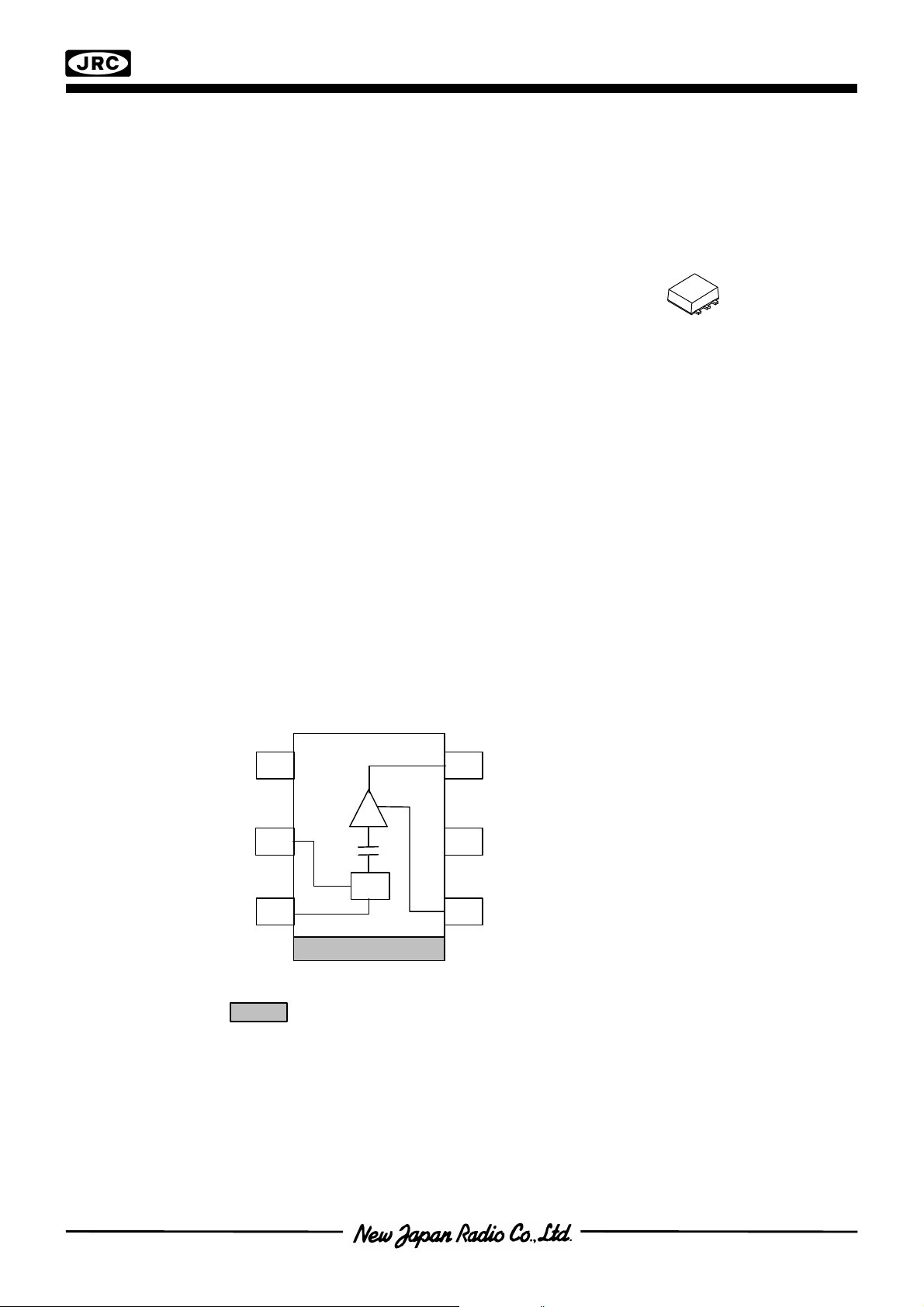
GENERAL DESCRIPTION nPACKAGE OUTLINE
NJG1104KB2 is a variable gain low noise amplifier (LNA).
At 800MHz band, noise figure is 1.2dB, variable gain range
is 21dB and input 3rd order intercept point is +6dBm. These
characteristics are very suitable for CDMA cellular phone
application.
The variable attenuators placed in front of LNA realize wide
range of input power with low distortion.
Very small and thin FLP6-B2 package is adopted.
n
FEATURES
lLow voltage operation +2.8V typ.
lLow current consumption 6.0mA typ.
lHigh gain 15dB typ. @f=865MHz
lLow noise figure 1.2dB typ. @f=865MHz
lVariable gain control 21dB typ. @f=865MHz,V
lHigh input IP3 +6dBm typ. @f=865.0+865.1MHz, Pin=-30dBm
lHigh output IP3 +21dBm typ. @f=865.0+865.1MHz, Pin=-30dBm
lUltra small & ultra thin package FLP6-B2 (Mount Size: 2.1x2.0x0.75mm)
=0.2 to 1.7V
CONT
n
PIN CONFIGURATION
KB2 Type
(Top View)
4
3
Pin Connection
1.SOURCE
AMP
5
2
2.GND
3.RFout
4.GND
ATT
6
5.VCONT
6.RFin
- 1 -
Page 2
NJG1104KB2
n
ABSOLUTE MAXIMUM RATINGS
( Ta=25°C, Zs=Zl=50Ω )
PARAMETER SYMBOL CONDITIONS RATINGS UNITS
Drain Voltage V
Gain Control Voltage V
CONT
Input Power P
Power Dissipation P
Operating Temperature T
Storage Temperature T
n
ELECTRICAL CHARACTERISTICS
DD
opr
stg
in
D
VDD=2.8V +20 dBm
(VDD =2.8V, V
=1.7V, f=865MHz, Ta=25°C, Zs=Zl=50Ω )
CONT
6.0 V
4.0 V
450 mW
-40~+85 °C
-55~+125 °C
PARAMETER SYMBOL CONDITIONS MIN TYP MAX UNITS
Operating Frequency freq 830 865 900 MHz
Drain Voltage V
Gain Control Voltage V
Operating Current I
Gain Control Terminal
Current
I
DD
CONT
DD
CONT
No RF Signal - 6.0 7.5 mA
No RF Signal - 1.0 5.0 uA
2.7 2.8 5.5 V
0.2 1.7 3.0 V
Small Signal Gain Gain 13.0 15.0 17.0 dB
Gain Flatness G
Gain Control Range G
flat
CONT
f=830~900MHz
V
=0.2V, 1.7V 18.5 20.5 22.5 dB
CONT
- 0.5 1.0 dB
Noise Figure NF - 1.20 1.40 dB
Pout at 1dB Gain
Compression point
Output 3rd Order
Intercept Point
Input 3rd Order
Intercept Point 1
Input 3rd Order
Intercept Point 2
RF Input Port VSWR VSWR
RF Output Port VSWR VSWR
P
-1dB
OIP3
IIP3-1
IIP3-2
f=865.0+865.1MHz
Pin=-30dBm
f=865.0+865.1MHz
Pin=-30dBm
f=865.0+865.1MHz
Pin=-10dBm
V
=0.2V
CONT
i
o
- +8.0 - dBm
+19.0 +21.0 - dBm
+4.0 +6.0 - dBm
+21.0 +26.0 - dBm
- 1.5 2.0 -
- 1.5 2.0 -
- 2 -
Page 3
NJG1104KB2
n
TERMINAL INFORMATION
Pin Function Description
This terminal is internally connected to FET’s source of LNA. Please connect self-
1 SOURCE
2, 4 GND
3 RFout
bias resistor (R1) and bypass capacitor (C3) through source inductor (L5). NF and
IIP3 are tunable by C3 and L5.
Ground (0V) terminal. Ground plane should be placed as close to the ground
terminals. .
RF output and drain voltage supplies terminal. External matching circuit is
required.
5 VCONT
6 RFin
Gain control voltage (V
RF input terminal. External matching circuit and DC blocking capacitor are required.
) supplies terminal.
CONT
Page 4
NJG1104KB2
n
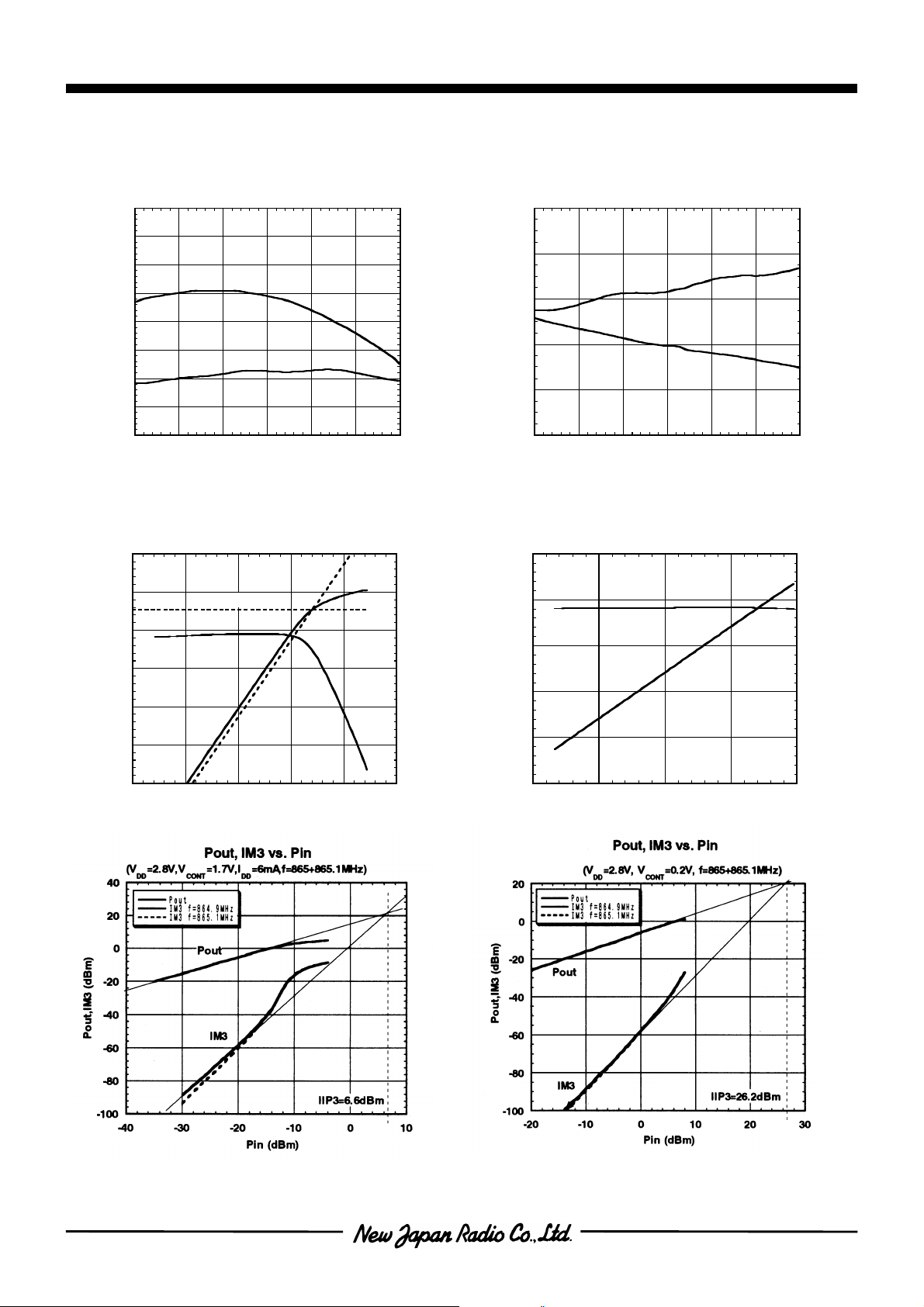
TYPICAL CHARACTERISTICS
NF,Gain vs. frequency
4.0
3.5
3.0
2.5
2.0
NF (dB)
1.5
1.0
0.5
0.0
700 750 800 850 900 950 1000
Gain
NF
(VDD=2.8V,V
frequency (MHz)
=1.7V,IDD=6mA)
CONT
Pout,Gain vs. Pin
15
10
5
0
Pout (dBm)
-5
-10
(VDD=2.8V,V
P-1dB=7.7dBm
Gain
Pout
=1.7V,f=865MHz)
CONT
18
17
16
15
14
13
12
11
10
20
15
10
Gain (dB)
Gain (dB)
NF,Gain vs. frequency
20
18
16
NF (dB)
14
12
10
700 750 800 850 900 950 1000
(VDD=2.8V,V
NF
Gain
frequency (MHz)
=0.2V,IDD=6mA)
CONT
Pout,Gain vs. Pin
(VDD=2.8V,V
10
0
Gain
-10
Pout (dBm)
-20
Pout
-30
=0.2V,f=865MHz)
CONT
0
-2
-4
-6
-8
-10
0
-5
-10
-15
-20
Gain (dB)
Gain (dB)
-15
-40 -30 -20 -10 0 10
Pin (dBm)
5
-40
-30 -20 -10 0 10
Pin (dBm)
-25
- 4 -
Page 5

NJG1104KB2
n
TYPICAL CHARACTERISTICS
NF,Gain vs. VCONT
30
25
20
15
NF (dB)
10
5
0
0.0 0.5 1.0 1.5 2.0
(VDD=2.8V, f=865MHz)
Gain
NF
VCONT (V)
NF,Gain vs. IDD
2.0
1.5
(VDD=2.8V,V
=1.7V,f=865MHz)
CONT
Gain
20
15
10
5
0
-5
-10
Gain (dB)
16
15
OIP3,IIP3 vs. VCONT
(VDD=2.8V,IDD=6mA,f=865+865.1MHz,Pin=-30dBm)
25
20
OIP3 (dBm)
15
10
0.0 0.5 1.0 1.5 2.0
VCONT (V)
OIP3,IIP3 vs. IDD
(VDD=2.8V,V
25
20
=1.7V,f=865+865.1MHz,Pin=-30dBm)
CONT
OIP3
20
OIP3
15
IIP3 (dBm)
10
IIP3
5
15
10
1.0
NF (dB)
0.5
0.0
4 5 6 7 8 9 10
IDD (mA)
Rbias vs. IDD
(VDD=2.8V, V
200
180
160
140
120
Rbias (ohm)
100
80
NF
CONT
=1.7V)
14
13
12
Gain (dB)
OIP3 (dBm)
15
10
4 5 6 7 8 9 10
Equations of OIP3 and IIP3
=3OIP
2
Gain-3OIP=3IIP
VCONT=1.7V@ Pin=-30dBm
VCONT=0.2V@ Pin=-10dBm
IIP3
IIP3 (dBm)
5
0
IDD (mA)
3IM-Pout×3
60
3 4 5 6 7 8 9 10 11
IDD (mA)
Page 6

NJG1104KB2
n
TYPICAL CHARACTERISTICS
NF,Gain vs. VDD
(V
=1.7V,f=865MHz)
2.0
1.8
1.6
NF (dB)
1.4
1.2
1.0
2.5 3.0 3.5 4.0 4.5 5.0 5.5 6.0
Gain
NF
CONT
VDD (V)
IDD vs. VDD
7.0
6.8
OIP3,IIP3 vs. VDD
(V
=1.7V,f=865+865.1MHz,Pin=-30dBm)
OIP3
IIP3
CONT
15
10
IIp3 (dBm)
5
0
VDD (V)
20
18
16
14
12
10
Gain (dB)
25
20
OIP3 (dBm)
15
10
2.5 3.0 3.5 4.0 4.5 5.0 5.5 6.0
OIP3,IIP3 vs. frequency
(V
=1.7V)
CONT
(VDD=2.8V,V
23
22
=1.7V,f1=freq,f2=freq+100kHz,Pin=-30dBm)
CONT
OIP3
10
9
6.6
IDD (mA)
6.4
6.2
6.0
2.5 3.0 3.5 4.0 4.5 5.0 5.5 6.0
VDD
IDD vs. Ta
(VDD=2.8V,V
10
9
8
IDD (mA)
7
6
CONT
=1.7V)
21
20
OIP3 (dBm)
19
18
820 840 860 880 900 920
IIP3
frequency (MHz)
Equations of OIP3 and IIP3
=3OIP
3IM-Pout×3
2
Gain-3OIP=3IIP
VCONT=1.7V@ Pin=-30dBm
VCONT=0.2V@ Pin=-10dBm
8
7
6
5
IIP3 (dBm)
5
-50 0 50 100
- 6 -
Ta (oC)
Page 7

NJG1104KB2
n
TYPICAL CHARACTERISTICS
Gain vs. Ta (Variable VCONT)
20
15
10
Gain (dB)
-5
-10
Delta Gain(max)=1.3dB@Ta=-40to80oC,VCONT=1.3V
VCONT=1.4V
VCONT=1.3V
VCONT=1.2V
VCONT=1.1V
5
0
VCONT=0.6V
VCONT=0.4V
VCONT=0.2V
-50 0 50 100
(VDD=2.8V,freq=865MHz)
VCONT=1.0V
VCONT=0.9V
VCONT=0.8V
VCONT=0V
Ta (oC)
NF,Gain vs. Ta
5
4
3
NF (dB)
2
1
0
-50 0 50 100
(VDD=2.8V,V
=1.7V,freq=865MHz)
CONT
Gain
NF
Ta (oC)
OIP3,IIP3 vs. Ta
(VDD=2.8V,V
30
28
26
=1.7V,freq=865+865.1MHz,Pin=-30dBm)
CONT
IIP3
20
18
16
14
12
10
10
8
6
Gain (dB)
NF,Gain vs. Ta
20
18
16
NF (dB)
14
12
10
-50 0 50 100
(VDD=2.8V,V
=0.2V,freq=865MHz)
CONT
NF
Gain
Ta (oC)
OIP3,IIP3 vs. Ta
(VDD=2.8V,V
26
24
22
=0.2V,freq=865+865.1MHz,Pin=-10dBm)
CONT
IIP3
0
-2
-4
-6
-8
-10
28
26
24
Gain (dB)
24
OIP3 (dBm)
22
OIP3
20
-50 0 50 100
Ta (oC)
4
2
0
IIP3 (dBm)
20
OIP3 (dBm)
18
16
-50 0 50 100
OIP3
Ta (oC)
22
20
18
IIP3 (dBm)
Page 8

NJG1104KB2
n
TYPICAL CHARACTERISTICS
S11,S21,S12,S22 vs. frequency
(VDD=2.8V,V
20
10
0
-10
-20
S11,S22,S21 (dB)
-30
-40
0 500 1000 1500 2000
S21
S22
S11
S12
frequency (MHz)
=1.7V,IDD=6mA)
CONT
S11,S22 vs. frequency
0
(VDD=2.8V,V
-5
=1.7V,IDD=6mA)
CONT
30
20
10
0
-10
-20
-30
S12 (dB)
S11,S21,S12,S22 vs. frequency
(VDD=2.8V,V
0
-5
-10
S11,S22,S21 (dB)
-15
-20
0 500 1000 1500 2000
S11
S12
frequency (MHz)
=0.2V,IDD=6mA)
CONT
S22
S21
S11,S22 vs. frequency
0
(VDD=2.8V,V
-5
=0.2V,IDD=6mA)
CONT
20
10
0
-10
-20
-30
-40
-50
-60
S12 (dB)
-10
S11,S22 (dB)
-15
S11
-20
0 5 10 15 20
S22
frequency (GHz)
S21,S12 vs. frequency
20
S21
10
0
-10
S21 (dB)
-20
-30
0 5 10 15 20
(VDD=2.8V,V
S12
frequency (GHz)
=1.7V,IDD=6mA)
CONT
20
10
0
-10
-20
-30
S12 (dB)
-10
S11,S22 (dB)
-15
-20
0 5 10 15 20
S22
frequency (GHz)
S11
S21,S12 vs. frequency
0
S21
-10
-20
-30
-40
S21 (dB)
-50
-60
-70
0 5 10 15 20
(VDD=2.8V,V
frequency (GHz)
S12
=0.2V,IDD=6mA)
CONT
10
0
-10
-20
-30
-40
-50
-60
S12 (dB)
- 8 -
Page 9

NJG1104KB2
n
TYPICAL CHARACTERISTICS
Scattering Parameter Table at Maximum Gain
VDD=2.8V, V
Freq
mag
(MHz)
100 0.990 -3.7 2.893 -162.9 0.011 94.9 0.795 -9.3
200 0.983 -7.0 3.258 171.6 0.008 56.3 0.725 -7.2
300 0.967 -9.9 3.125 154.6 0.011 85.4 0.744 -5.8
400 0.946 -12.5 2.910 141.2 0.014 84.2 0.770 -6.8
500 0.927 -14.8 2.648 130.2 0.020 87.7 0.792 -8.8
600 0.909 -16.8 2.407 120.6 0.025 87.5 0.819 -11.5
700 0.896 -18.5 2.182 112.6 0.029 84.5 0.835 -14.5
800 0.884 -19.9 1.975 105.2 0.034 81.0 0.849 -17.6
900 0.876 -21.3 1.790 98.9 0.039 78.6 0.864 -20.8
1000 0.871 -22.7 1.624 92.9 0.044 77.3 0.874 -24.0
1100 0.867 -24.1 1.480 87.4 0.048 73.1 0.880 -27.2
1200 0.864 -25.3 1.349 82.2 0.054 71.6 0.884 -30.5
1300 0.860 -26.8 1.234 77.4 0.059 68.3 0.891 -33.8
1400 0.861 -28.1 1.129 72.7 0.063 66.2 0.897 -37.1
1500 0.862 -29.7 1.029 68.2 0.068 63.8 0.903 -40.4
1600 0.862 -31.3 0.942 63.8 0.072 61.0 0.907 -43.8
1700 0.863 -33.0 0.860 59.4 0.078 57.7 0.912 -47.4
1800 0.867 -34.7 0.783 55.2 0.083 55.4 0.916 -50.6
1900 0.869 -36.5 0.713 51.1 0.087 52.4 0.920 -54.0
2000 0.874 -38.4 0.650 47.3 0.091 50.5 0.921 -57.6
(units)
=1.7V, IDD=6.1mA, Zo=50Ω
CONT
S11 S21 S12 S22
ang
(deg)
mag
(units)
ang
(deg)
mag
(units)
ang
(deg)
mag
(units)
ang
(deg)
Reference Plane
GND
4
V
CONT
Network Analyzer
Port1
Note
=1.7V
1000p
Reference Plane
VDD (=2.8V) is supplied through “BIAS CONNECT (PORT2)” of Network Analyzer.
Vcont
5
RFin
6
AMP
ATT
3
RFout
GND
2
SOURCE
1
5.6n
1000p
120
Network Analyzer
Port2
Page 10

NJG1104KB2
n
TYPICAL CHARACTERISTICS
Scattering Parameter Table at Minimum Gain
VDD=2.8V, V
Freq
mag
(MHz)
100 0.771 -62.4 2.226 171.8 0.002 -94.5 0.784 -9.3
200 0.573 -99.1 1.803 141.7 0.004 25.2 0.728 -6.5
300 0.480 -121.8 1.405 128.1 0.005 37.2 0.744 -4.9
400 0.430 -138.2 1.151 119.5 0.003 70.3 0.774 -5.6
500 0.405 -150.1 0.975 113.2 0.007 67.3 0.801 -7.5
600 0.391 -159.8 0.849 107.8 0.007 67.3 0.829 -10.2
700 0.381 -167.4 0.749 103.2 0.009 76.9 0.850 -13.2
800 0.373 -174.5 0.666 99.0 0.010 70.2 0.867 -16.4
900 0.369 179.3 0.597 95.3 0.013 75.7 0.884 -19.8
1000 0.366 173.4 0.538 91.7 0.014 73.3 0.897 -23.1
1100 0.365 168.5 0.489 88.4 0.015 74.7 0.905 -26.4
1200 0.365 163.1 0.443 84.9 0.017 73.9 0.910 -29.8
1300 0.367 158.7 0.406 81.9 0.019 70.8 0.918 -33.2
1400 0.369 154.2 0.371 78.8 0.020 68.7 0.923 -36.7
1500 0.372 150.2 0.338 76.0 0.021 65.2 0.930 -40.0
1600 0.374 146.3 0.310 73.1 0.023 63.8 0.932 -43.4
1700 0.378 142.6 0.283 70.6 0.024 64.2 0.938 -47.0
1800 0.384 139.1 0.257 67.8 0.026 63.6 0.942 -50.4
1900 0.388 136.5 0.232 64.7 0.027 60.2 0.944 -53.9
2000 0.388 133.1 0.211 62.7 0.029 59.5 0.947 -57.6
(units)
=0.2V, IDD=6.1mA, Zo=50Ω
CONT
S11 S21 S12 S22
ang
(deg)
mag
(units)
ang
(deg)
mag
(units)
ang
(deg)
mag
(units)
ang
(deg)
Reference Plane
GND
4
V
CONT
Network Analyzer
Port1
Note
=0.2V
1000p
Reference Plane
VDD (=2.8V) is supplied through “BIAS CONNECT (PORT2)” of Network Analyzer.
Vcont
5
RFin
6
AM P
ATT
3
RFout
GND
2
SOURCE
1
5.6n
1000p
Network Analyzer
Port2
120
- 10 -
Page 11

NJG1104KB2
n
CONTVDD
RECOMMENDED CIRCUIT
V
CONT
=0.2V to 1.7V
RF Input
L1
n
RECOMMENDED PCB DESIGN
C1
V
L2
C5
GND
4
Vcont
5
RFin
6
C4
AMP
ATT
RFout
3
GND
2
SOURCE
1
L3
L5
C2
RF Output
L4
VDD=2.8V
C4
R1
C3
L4
L3
C3
C2
L5
R1
C5
RF Input
Parts List (f=830~900MHz)
PARTS ID Constant Comment
L1 22nH TAIYO-YUDEN HK1005 Series
L2 22nH TAIYO-YUDEN HK1608 Series
L3 22nH TAIYO-YUDEN HK1005 Series
L4 15nH TAIYO-YUDEN HK1005 Series
L5 5.6nH TAIYO-YUDEN HK1005 Series
C1, C4, C5 1000pF MURATA GRM36 Series
L1
L2
C1
RF Output
PCB: FR4 t=0.2mm
MICROSTRIP LINE WIDTH=0.4mm(Zo=50Ω)
PCB SIZE: 20.0x20.0mm
PRECAUTIONS
1) The inductor of 1608 size is
recommended for NF
characteristics.
2) The value of C3 is selected
to get lower gain and higher
output IP3.
C2 6pF MURATA GRM36 Series
C3 100pF MURATA GRM36 Series
R1
120Ω
-
Page 12

NJG1104KB2
n
• To waste this product, please obey the relating law of your country.
with care to avoid these damages .
[CAUTION]
PACKAGE OUTLINE (FLP6-B2)
2.0±0.1
6 5 4
1 2 3
0.65 0.65
+0.1
0.2-0.05
0.75±0.05
0.20.2
2.1±0.1
1.7±0.1
+0.1
0.15-0.05
Lead material : Copper
Lead surface finish: Solder plating
Molding material : Epoxy resin
0.1 0.1
UNIT : mm
Weight : 6.5mg
Cautions on using this product
This product contains Gallium-Arsenide (GaAs) which is a harmful material.
• Do NOT eat or put into mouth.
• Do NOT dispose in fire or break up this product.
• Do NOT chemically make gas or powder with this product.
This product may be damaged with electric static discharge (ESD) or spike voltage. Please handle
- 12 -
The specifications on this databook are only
given for information , without any guarantee
as regards either mistakes or omissions. The
application circuits in this databook are
described only to show representative usages
of the product and not intended for the
guarantee or permission of any right including
the industrial rights.
 Loading...