


THIS DOCUMENT IS FOR MAINTENANCE
PURPOSES ONLY AND IS NOT
RECOMMENDED FOR NEW DESIGNS
NJ88C30 IS FOR MAINTENANCE PURPOSES ONLY AND IS NOT RECOMMENDED FOR NEW DESIGNS
NJ88C30
VHF SYNTHESISER
T
he NJ88C30 contains all the logic needed for a VHF PLL
synthesiser and is fabricated on the GPS high performance, small
geometry CMOS process. The circuit contains a reference oscillator
and divider, a two-modulus prescaler and 4-bit control register, a
12-bit programmable divider, a phase comparator and the
necessary data input and control logic.
FEATURES
■
Low Power CMOS
■ Easy to Use
■
Low Cost
■
Single Chip Synthesiser to VHF
■
Lock Detect Output
APPLICATIONS
■
Mobile Radios
■ Hand Held Portable Radios
■
Sonobuoys
ORDERING INFORMATION
NJ88C30 KA DP Plastic DIL Package
NJ88C30 KA MP Miniature Plastic DIL Package
GROUND
DATA TRANSFER
CLOCK
DATA
CRYSTAL MON
CRYSTAL IN
CRYSTAL OUT
1
2
3
4
NJ88C30
5
6
7
14
13
12
11
10
9
8
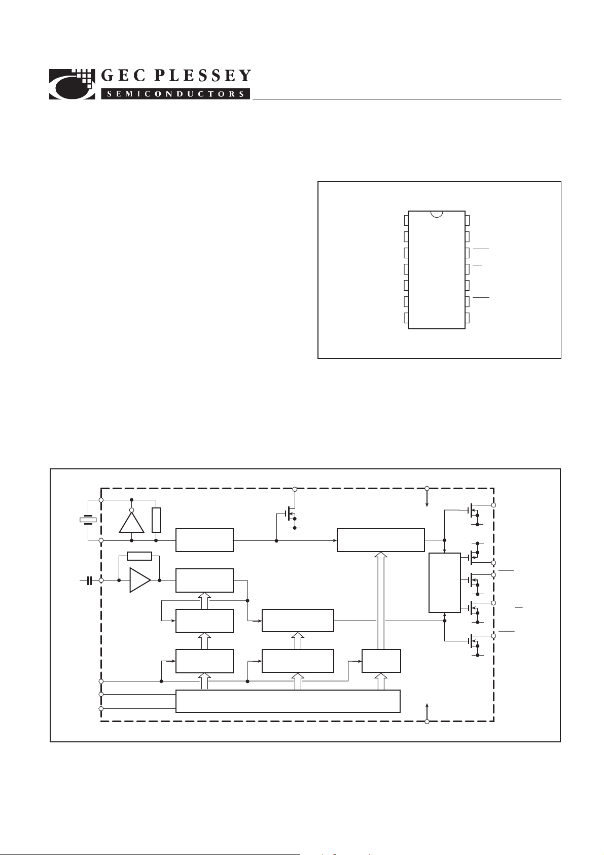
Fig.1 Pin connections - top view
ABSOLUTE MAXIMUM RATINGS
Supply voltage, V
Voltage on any pin
Operating temperature
Storage temperature
DD
NJ88C30
DS3281-1.1
COMP FREQ
f UP
f DN
LD
VCO
P DIV OUT
V
DD
DP14, MP14
20·3V to 6V
20·3V to V
230°C to 170°C
255°C to 1125°C
DD
10·3V
CRYSTAL
OUT
CRYSTAL
IN
VCO
DATA
TRANSFER
DATA
CLOCK
V
CRYSTAL MON
7
6
10
2
4
3
4 100
4 15/16
4-BIT COUNTER
4-BIT REGISTER
12-BIT PROG DIVIDER
19-BIT SHIFT REGISTER
5
0V
12-BIT REGISTER
REFERENCE DIVIDER
4 1, 5, 10, 20, 2, 4, 8 OR 16
REF
SELECT
(DR2-DR0)
3-BIT
REGISTER
DD
8
PHASE
1
GROUND
COMP
14
COMP FREQ
0V
V
DD
13
f UP
12
f DN
0V
11
LOCK DETECT
(LD)
0V
9
P DIV OUT
0V
Fig.2 Block diagram
NJ88C30
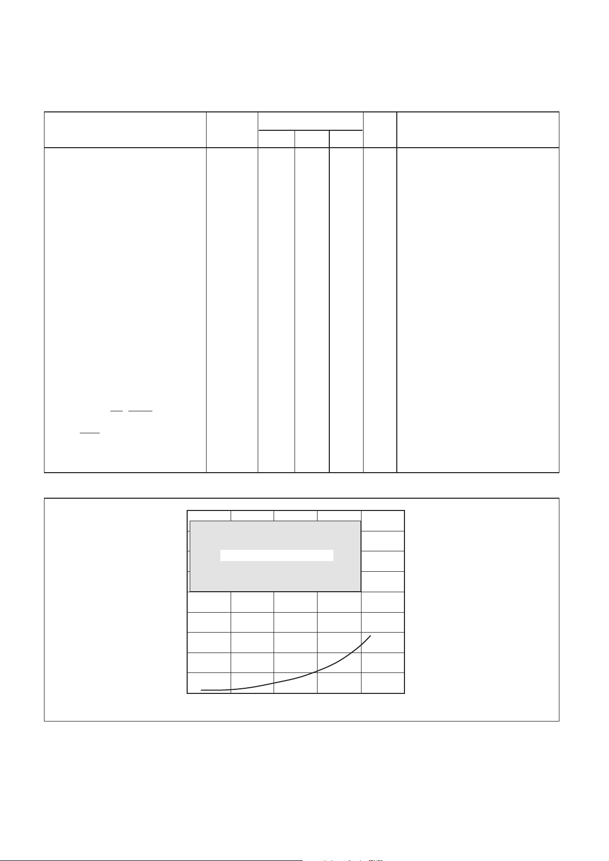
ELECTRICAL CHARACTERISTICS
Test conditions (unless otherwise stated):
T
= –30°C to +70°C, VDD = 5V ±0·5V
AMB
Characteristic
Pin
Min.
Value
Typ. Max.
Units
Conditions
Supply current
Crystal Oscillator
Frequency
External input level
High level
Low level
VCO Input
Input sensitivity
Slew rate
Input impedance
DATA, DATA TRANSFER and
CLOCK Inputs
High level
Low level
Rise, fall time
Data set-up time
Clock frequency
Transfer pulse width
CRYSTAL MONITOR Output
Current sink
COMP FREQ,
LD, P DIV
Current sink
f UP / f DN
Current sink
Current source
8
6, 7
6
6
6
10
10
10
2, 3, 4
2. 3, 4
2, 3
3, 4
3
2
5
9, 11, 14
12
13
V
V
1
DD
1
4
DD
200
500
0·8
1·6
0·8
0·8
21
21
4
10
5pF//
10k
7
15
1
1
200
2
mA
MHz
Vrms
V
V
Vrms
V/µs
V
V
ns
ns
MHz
ns
mA
mA
mA
mA
1VRMS VCO input at 200MHz
XTAL
= 10MHz
and f
Parallel resonant,
fundamental crystal
AC coupled
DC coupled
DC coupled
At 200MHz, see Fig. 3
See Fig. 4
= 0·5V
V
OUT
V
= 0·5V
OUT
V
= 0·5V
OUT
= VDD20·5V
V
OUT
1·6
1·4
1·2
1·0
0·8
0·6
VCO INPUT AMPLITUDE (V RMS)
0·4
0·2
0
0 50 100 150 200
GUARANTEED OPERATING AREA *
* Tested as
specified in
Table of
Electrical
Characteristics
TYPICAL
FREQUENCY (MHz)
Fig. 3 Input sensitivity
2

CLOCK
NJ88C30
DATA
DATA SET-UP TIME
DATA
TRANSFER
20
10
0
GAIN (dB)
210
100k 1M 10M
DR2
FREQUENCY (Hz)
DR1 DR0 DF15 DF1 DF0
TRANSFER PULSE WIDTH
Fig. 4 Input data timing diagram
180
120
60
PHASE (DEGREES)
0
100k 1M 10M
FREQUENCY (Hz)
Fig. 5 Gain and phase characteristics of reference oscillator inverter
CIRCUIT DESCRIPTION
Crystal Oscillator and Reference Divider
The Reference oscillator consists of a Pierce type oscillator
intended for use with a parallel resonant fundamental crystal.
Typical gain and phase characteristics for the oscillator inverter
are shown in Fig 5. An external reference oscillator may be
used by either capacitively coupling a 1V RMS sinewave into
CRYSTAL IN (pin 6) or, if CMOS levels are available, by direct
connection to CRYSTAL IN.
The reference oscillator drives a 4100 prescaler followed
by a reference divider to provide a range of comparison
frequencies which are selected by decoding the first three bits
(DR2, DR1, DR0) of the input data. The possible division ratios
and the comparison frequencies (channel spacing) if a 10MHz
crystal is used are shown in Table 1.
DR2
0
0
0
0
1
1
1
1
Total
DR1
DR0
division
ratio
0
0
1
0
0
1
1
1
0
0
1
0
0
1
1
1
1600
800
400
200
2000
1000
500
100
Table 1 Reference divider division ratios
Comparison frequency
for 10MHz Ref. Osc.
6·25kHz
12·5kHz
25kHz
50kHz
5kHz
10kHz
20kHz
100kHz
To assist in trimming the crystal, an open drain output at one
hundredth of the reference oscillator frequency is provided on
CRYSTAL MONITOR pin 5
Programmable Divider
The programmable divider consists of a 415/16 two modulus
prescaler with a 4-bit control register, followed by a 12-bit
programmable divider. A 1V RMS sinewave should be
capacitively coupled from the VCO to the divider input VCO pin
(pin 10).
The overall division ratio is selected by a single 16-bit word
(DF15 to DF0), loaded through the serial data bus. A lower limit
of 240 ensures correct prescaler operation; the upper limit is
65535. The VCO frequency in a locked system will be this
division ratio multiplied by the comparison frequency.
Phase Comparator
The phase comparator consists of a digital type phase
comparator with open drain f UP and f DN outputs and an
open drain LOCK DETECT (
LD) output. Open drain outputs
from the reference divider and programmable divider are
provided for monitoring purposes or for use with an external
phase comparator. Waveforms for all these outputs are shown
in Fig.6. The duty cycle of f UP and f DN versus phase
difference are shown in Fig. 7. The phase comparator is linear
over a ±2π range and if the phase gains or slips by more than
2π, the phase comparator outputs repeat with a 2π period.
3

NJ88C30
(a) Phase P DIV output leads
phase COMP FREQ output
(b) Phase P DIV output lags
phase COMP FREQ output
COMP FREQ
P DIV
f UP
f DN
LD
COMP FREQ
P DIV
f UP
f DN
LD
22π
Fig. 6 Phase comparator waveforms
DUTY CYCLE
f UP
100%
0%
DUTY CYCLE
f DN
100%
2π0
PHASE DIFFERENCE
0%
22π
0
2π
PHASE DIFFERENCE
Fig. 7 Phase comparator output characteristics
4

NJ88C30
Once the phase difference exceeds 2π, the comparator will
gain or slip one cycle and then try to lock on to the new zero
phase difference. Note that very narrow pulses may be seen on
the inactive phase comparator output at the end of the pulse on
the active output, as shown in Fig. 6.
Data Input and Control Register
To control the synthesiser a simple three-line serial input is
used with DATA, CLOCK and DATA TRANSFER signals. The
data consists of 19 bits; the first three, DR2, DR1 and DR0,
control the reference divider while the following sixteen, DF15
LOCK DETECT (LD)
14
13
12
11
10
9
8
R1 18k
R1' 18k
22k
10n
15V
DATA TRANSFER
CLOCK
DATA
4·5MHz
5 - 65p
1
2
3
4
NJ88C30
5
6
7
to DF0, control the prescaler and programmable divider. Until
the synthesiser receives the DATA TRANSFER pulse, it will
use the previously loaded data; on receiving the pulse it will
switch rapidly to the new data.
APPLICATIONS
A simplified circuit for a synthesiser intended for VHF
broadcast receiver applications is shown in Fig. 8. When the
varicap line drive voltage necessary to tune the required band
is greater than 5V, some form of level shifter such as the
operational amplifier shown in Fig. 8 is required.
112V
R2
10k
47n
1
SL562
2
C1
22k
22k
10k
10n
VARICAP DRIVE
1 -10V
VCO
112V
Fig.8. Typical application
PROGRAMMING EXAMPLE
1.Maximum Frequency
For a channel spacing (comparison frequency, f
5kHz when using a 10MHz crystal oscillator, the reference
divider ratio will need to be 2000 (seeTable 1) This is
programmed as binary 100 (= 4
) in the most significant
HEX
three of the 19 bits (MSB programmed first).
DR DF
2101514131211109876543210
Binary 1001001110001000000
Hex 49 C 4 0
Table 2 Maximum VCO frequency programming (f
2. Minimum Frequency
Using the same crystal frequency and channel spacing
(10MHz, 5kHz), the lower limit of programmable divider ratio of
DR DF
2101514131211109876543210
Binary 1000000000011110000
Hex 400F0
Table 3 MinimumVCO frequency programming (f
comp
) of
To obtain the maximum VCO frequency of 200MHz the
programmable divider ratio would be:
5310
6
= 40310
3
3
which is 9C40
HEX
200310
The program word would then be as shown in Table 2.
XTAL
240 = F0
of 24035310
HEX
= 10MHz, f
gives a minimum programmable VCO frequency
3
= 1·2MHz. The program word for this frequency
comp
= 5kHz)
is therefore as shown in Table 3.
= 10MHz, f
XTAL
comp
= 5kHz)
5

NJ88C30
HEADQUARTERS OPERATIONS
GEC PLESSEY SEMICONDUCTORS
Cheney Manor, Swindon,
Wiltshire SN2 2QW, United Kingdom.
Tel: (0793) 518000
Fax: (0793) 518411
GEC PLESSEY SEMICONDUCTORS
P.O. Box 660017
1500 Green Hills Road,
Scotts Valley, California 95067-0017,
United States of America.
Tel: (408) 438 2900
Fax: (408) 438 5576
CUSTOMER SERVICE CENTRES
• FRANCE & BENELUX Les Ulis Cedex Tel: (1) 64 46 23 45 Tx: 602858F
Fax : (1) 64 46 06 07
• GERMANY Munich Tel: (089) 3609 06-0 Tx: 523980 Fax : (089) 3609 06-55
• ITALY Milan Tel: (02) 66040867 Fax: (02) 66040993
• JAPAN Tokyo Tel: (03) 3296-0281 Fax: (03) 3296-0228
• NORTH AMERICA Integrated Circuits and Microwave Products Scotts Valley, USA
Tel (408) 438 2900 Fax: (408) 438 7023.
Hybrid Products, Farmingdale, USA Tel (516) 293 8686
Fax: (516) 293 0061.
• SOUTH EAST ASIA Singapore Tel: (65) 3827708 Fax: (65) 3828872
• SWEDEN Stockholm, Tel: 46 8 702 97 70 Fax: 46 8 640 47 36
• UNITED KINGDOM & SCANDINAVIA
Swindon Tel: (0793) 518510 Tx: 444410 Fax : (0793) 518582
These are supported by Agents and Distributors in major countries world-wide.
GEC Plessey Semiconductors 1992 Publication No. DS3281 Issue No. 1.1 May 1992
This publication is issued to provide information only which (unless agreed by the Company in writing) may not be used, applied or reproduced for any purpose nor form part of any order or contract nor to be regarded
as a representation relating to the products or services concerned. No warranty or guarantee express or implied is made regarding the capability, performance or suitability of any product or service. The Company
reserves the right to alter without prior knowledge the specification, design or price of any product or service. Information concerning possible methods of use is provided as a guide only and does not constitute
any guarantee that such methods of use will be satisfactory in a specific piece of equipment. It is the user's responsibility to fully determine the performance and suitability of any equipment using such information
and to ensure that any publication or data used is up to date and has not been superseded. These products are not suitable for use in any medical products whose failure to perform may result in significant injury
or death to the user. All products and materials are sold and services provided subject to the Company's conditions of sale, which are available on request.
 Loading...