

Page 1
NIF62514
Preferred Device
Self-Protected FET
with Temperature and
Current Limit
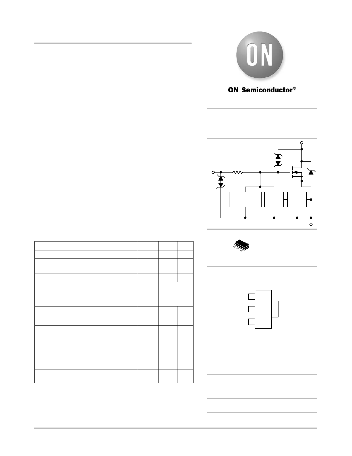
HDPlus devices are an advanced series of power MOSFETs which
utilize ON Semiconductor's latest MOSFET technology process to
achieve the lowest possible on-resistance per silicon area while
incorporating smart features. Integrated thermal and current limits
work together to provide short circuit protection. The devices feature
an integrated Drain-to-Gate Clamp that enables them to withstand
high energy in the avalanche mode. The Clamp also provides
additional safety margin against unexpected voltage transients.
Electrostatic Discharge (ESD) protection is provided by an integrated
Gate-to-Source Clamp.
Features
•Current Limitation
•Thermal Shutdown with Automatic Restart
•Short Circuit Protection
•Low R
•I
•Avalanche Energy Specified
•Slew Rate Control for Low Noise Switching
•Overvoltage Clamped Protection
•Pb-Free Packages are Available
DS(on)
Specified at Elevated Temperature
DSS
Gate
Input
http://onsemi.com
6.0 AMPERES*
40 VOLTS CLAMPED
R
DS(on)
R
G
ESD Protection
Temperature
Limit
= 90 mW
Overvoltage
Protection
Current
Limit
Drain
Current
Sense
Source
M
PWR
MOSFET MAXIMUM RATINGS (T
Rating Symbol Value Unit
Drain-to-Source Voltage Internally Clamped V
Drain-to-Gate Voltage Internally Clamped
= 1.0 MW)
(R
GS
Gate-to-Source Voltage V
Drain Current
- Continuous @ T
- Continuous @ TA = 100°C
- Pulsed (t
Total Power Dissipation @ TA = 25°C (Note 1)
@ T
@ TA = 25°C (Note 3)
Thermal Resistance, Junction-to-Tab
Junction-to-Ambient (Note 1)
Junction-to-Ambient (Note 2)
Single Pulse Drain-to-Source Avalanche Energy
(V
DD
VDS = 40 Vdc, IL = 2.8 Apk, L = 80 mH,
R
G
Operating and Storage Temperature Range TJ, T
Stresses exceeding Maximum Ratings may damage the device. Maximum
Ratings are stress ratings only. Functional operation above the Recommended
Operating Conditions is not implied. Extended exposure to stresses above the
Recommended Operating Conditions may affect device reliability.
1. Mounted onto min pad board.
2. Mounted onto 1″ pad board.
3. Mounted onto large heatsink.
p
= 25°C (Note 2)
A
= 25 Vdc, VGS = 5.0 Vdc,
= 25 W)
A
≤ 10 ms)
= 25°C
= 25°C unless otherwise noted)
J
JT
stg
40 Vdc
40 Vdc
"16 Vdc
Internally
Limited
1.1
1.73
8.93
14
114
72.3
300 mJ
-55 to
150
V
I
R
R
R
E
DSS
DGR
GS
I
D
I
D
DM
P
D
q
q
JA
q
JA
AS
W
°C/W
°C
4
1
2
3
SOT-223
CASE 318E
STYLE 3
MARKING DIAGRAM
GATE
DRAIN
SOURCE
A = Assembly Location
Y = Year
W = Work Week
62514 = Specific Device Code
G = Pb-Free Package
(Note: Microdot may be in either location)
1
4
62514G
AYW
2
G
3
DRAIN
ORDERING INFORMATION
See detailed ordering and shipping information in the package
dimensions section on page 5 of this data sheet.
Preferred devices are recommended choices for future use
and best overall value.
*Limited by the current limit circuit.
© Semiconductor Components Industries, LLC, 2007
November, 2007 - Rev. 6
1 Publication Order Number:
NIF62514/D
Page 2
NIF62514
MOSFET ELECTRICAL CHARACTERISTICS (T
Characteristic
= 25°C unless otherwise noted)
J
Symbol Min Typ Max Unit
OFF CHARACTERISTICS
Drain-to-Source Clamped Breakdown Voltage
= 0 Vdc, ID = 250 mAdc)
(V
GS
= 0 Vdc, ID = 250 mAdc, TJ = 150°C)
(V
GS
Zero Gate Voltage Drain Current
(V
= 32 Vdc, VGS = 0 Vdc)
DS
(VDS = 32 Vdc, VGS = 0 Vdc, TJ = 150°C)
Gate Input Current
(V
= 5.0 Vdc, VDS = 0 Vdc)
GS
(VGS = -5.0 Vdc, VDS = 0 Vdc)
V
(BR)DSS
I
DSS
I
GSS
42
42
46
45
-
-
-
-
0.5
2.0
50
550
50
50
2.0
10
100
1000
ON CHARACTERISTICS
Gate Threshold Voltage
= VGS, ID = 150 mAdc)
(V
DS
Threshold Temperature Coefficient (Negative)
Static Drain-to-Source On-Resistance (Note 4)
(V
= 10 Vdc, ID = 1.4 Adc, TJ @ 25°C)
GS
(VGS = 10 Vdc, ID = 1.4 Adc, TJ @ 150°C)
Static Drain-to-Source On-Resistance (Note 4)
(V
= 5.0 Vdc, ID = 1.4 Adc, TJ @ 25°C)
GS
(VGS = 5.0 Vdc, ID = 1.4 Adc, TJ @ 150°C)
Source-Drain Forward On Voltage
(I
= 7 A, VGS = 0 V)
S
V
GS(th)
R
DS(on)
R
DS(on)
V
SD
1.0
-
-
-
-
-
1.7
4.0
90
165
105
185
2.0
6.0
100
190
120
210
- 1.05 - V
SWITCHING CHARACTERISTICS
Turn-on Delay Time 10% Vin to 10% I
RL = 4.7 W, Vin = 0 to 10 V, VDD = 12 V
Turn-on Rise Time 10% ID to 90% I
RL = 4.7 W, Vin = 0 to 10 V, VDD = 12 V
Turn-off Delay Time 90% Vin to 90% I
RL = 4.7 W, Vin = 10 to 0 V, VDD = 12 V
Turn-off Fall Time 90% ID to 10% I
RL = 4.7 W, Vin = 10 to 0 V, VDD = 12 V
Slew-Rate On
RL = 4.7 W,
Vin = 0 to 10 V, VDD = 12 V
Slew-Rate Off
RL = 4.7 W,
V
= 10 to 0 V, VDD = 12 V
in
D
D
D
D
t
d(on)
t
rise
t
d(off)
t
fall
-dVDS/dt
dVDS/dt
- 4.0 8.0
- 11 20
- 32 50
- 27 50
- 1.5 2.5
on
off
- 0.6 1.0
SELF PROTECTION CHARACTERISTICS (TJ = 25°C unless otherwise noted)
Current Limit
Current Limit (VGS = 10 Vdc)
Temperature Limit (Turn-off) VGS = 5.0 Vdc T
Temperature Limit (Circuit Reset) VGS = 5.0 Vdc T
Temperature Limit (Turn-off) VGS = 10 Vdc T
Temperature Limit (Circuit Reset) VGS = 10 Vdc T
(VGS = 5.0 Vdc)
(V
= 5.0 Vdc, TJ = 150°C)
GS
(V
= 10 Vdc, TJ = 150°C)
GS
I
LIM
I
LIM
LIM(off)
LIM(on)
LIM(off)
LIM(on)
6.0
3.0
7.0
4.0
9.0
5.0
10.5
7.5
11
8.0
13
10
150 175 200 °C
135 160 185 °C
150 155 185 °C
130 140 170 °C
ESD ELECTRICAL CHARACTERISTICS (TJ = 25°C unless otherwise noted)
Electro-Static Discharge Capability
Human Body Model (HBM) ESD 4000 - - V
Electro-Static Discharge Capability Machine Model (MM) ESD 400 - - V
4. Pulse Test: Pulse Width = 300 ms, Duty Cycle = 2%.
Vdc
mAdc
mAdc
Vdc
mV/°C
mW
mW
ms
ms
ms
ms
ms
ms
Adc
Adc
http://onsemi.com
2
Page 3

NIF62514
TYPICAL ELECTRICAL CHARACTERISTICS
12
10
8
6
4
DRAIN CURRENT (AMPS)
2
D,
I
0
135
VDS, DRAIN-TO-SOURCE VOLTAGE (VOLTS)
Figure 1. Output Characteristics Figure 2. Output Characteristics
14
12
10
8
6
4
DRAIN CURRENT (AMPS)
D,
I
2
0
0
135
, DRAIN-TO-SOURCE VOLTAGE (VOLTS)
V
DS
VGS = 10 V
5 V
4 V
3 V
42
VGS = 10 V
5 V
4 V
TJ = -40°C
42
7 V
6 V
TJ = 25°C
3 V
7 V
6 V
8
TJ = 150°C
7
6
5
4
3
2
DRAIN CURRENT (AMPS)
D,
I
1
0
6
0
V
12
VDS = 5 V
10
8
6
4
DRAIN CURRENT (AMPS)
D,
2
I
0
0.5 2.5 3 3.5
6
0
VGS = 10 V
7 V
6 V
5 V
4 V
3 V
1350
, DRAIN-TO-SOURCE VOLTAGE (VOLTS)
DS
42
TJ = -40°C
TJ = 25°C
TJ = 150°C
21.51
4 4.5 5
VGS, GATE-TO-SOURCE VOLTAGE (VOLTS)
6
Figure 3. Output Characteristics
250
225
200
VGS = 10 V
I
= 1.4 A
D
175
150
125
Maximum
100
75
Typical
50
25
, DRAIN-TO-SOURCE RESISTANCE (mW)
0
-50 50 75250 100-25 125
DS(on)
R
, JUNCTION TEMPERATURE (°C)
T
J
Figure 5. Drain-to-Source Resistance versus
Junction Temperature
250
225
200
175
150
125
100
75
50
25
, DRAIN-TO-SOURCE RESISTANCE (mW)
0
150
-50 50 75250 100-25 125
DS(on)
R
http://onsemi.com
3
Figure 4. Transfer Characteristics
VGS = 5 V
I
= 1.4 A
D
Maximum
Typical
, JUNCTION TEMPERATURE (°C)
T
J
Figure 6. Drain-to-Source Resistance versus
Junction Temperature
150
Page 4

NIF62514
4
VDS = 32 V
3
2
CURRENT (mA)
1
, DRAIN-TO-SOURCE LEAKAGE
DSS
I
Typical
0
-50 25 50075-25 100
TJ, JUNCTION TEMPERATURE (°C)
Figure 7. Drain-to-Source Resistance versus
Junction Temperature
12
10
8
125
150
Current Limit
VGS = 10 V
2.50
2.25
2.00
1.75
1.50
VTH + 4 Sigma
VTH - 4 Sigma
V
TH
1.25
1.00
0.75
0.50
0.25
GATE THRESHOLD VOLTAGE (V)
0
-50 7010-10-30 90 130
TEMPERATURE (°C)
Figure 8. Gate Threshold Voltage versus
Temperature
Temperature Limit
ID = 150 mA
15030 50 110
6
VGS = 5 V
4
DRAIN CURRENT (AMPS)
2
0
30512 4
TIME (ms)
Figure 9. Short-circuit Response
100
Duty Cycle = 0.5
0.2
10
0.1
0.05
D CURVES APPLY
FOR POWER
PULSE TRAIN SHOWN
READ TIME AT T
T
- TA = P
J(pk)
@ R(t) for t ≤ 0.02
R
2
q
JC
s
(pk)
0.1
P
0.02
1
0.01
Single Pulse
(pk)
t
1
t
2
DUTY CYCLE, D = t1/t
0.00001 0.0001 0.001 0.01 0.1 1 10
R(t), TRANSIENT THERMAL RESISTANCE (°C/W)
t,TIME (S)
Figure 10. Transient Thermal Resistance
(Non-normalized Junction-to-Ambient mounted on minimum pad area)
1
R
(t)
q
JA
http://onsemi.com
4
Page 5

NIF62514
ORDERING INFORMATION
Device Package Shipping
NIF62514T1 SOT-223
NIF62514T1G SOT-223
(Pb-Free)
NIF62514T3G SOT-223
(Pb-Free)
†For information on tape and reel specifications, including part orientation and tape sizes, please refer to our Tape and Reel Packaging
Specifications Brochure, BRD8011/D.
1000 / Tape & Reel
4000 / Tape & Reel
†
http://onsemi.com
5
Page 6

b1
NIF62514
PACKAGE DIMENSIONS
SOT-223 (TO-261)
CASE 318E-04
ISSUE M
D
NOTES:
1. DIMENSIONING AND TOLERANCING PER ANSI
Y14.5M, 1982.
2. CONTROLLING DIMENSION: INCH.
0.08 (0003)
e1
H
E
A1
4
123
e
E
b
q
A
C
DIMAMIN NOM MAX MIN
A1 0.02 0.06 0.10 0.001
b 0.60 0.75 0.89 0.024
b1 2.90 3.06 3.20 0.115
c 0.24 0.29 0.35 0.009
D 6.30 6.50 6.70 0.249
E 3.30 3.50 3.70 0.130
e 2.20 2.30 2.40 0.087
e1
L1 1.50 1.75 2.00 0.060
H
E
q
STYLE 3:
L1
MILLIMETERS
1.50 1.63 1.75 0.060
0.85 0.94 1.05 0.033
6.70 7.00 7.30 0.264
0° 10° 0° 10°
- -
PIN 1. GATE
2. DRAIN
3. SOURCE
4. DRAIN
INCHES
NOM MAX
0.064 0.068
0.002 0.004
0.030 0.035
0.121 0.126
0.012 0.014
0.256 0.263
0.138 0.145
0.091 0.094
0.037 0.041
0.069 0.078
0.276 0.287
SOLDERING FOOTPRINT
3.8
0.15
2.0
0.079
2.3
0.091
2.3
0.091
6.3
0.248
2.0
0.079
1.5
0.059
SCALE 6:1
ǒ
inches
mm
Ǔ
*For additional information on our Pb-Free strategy and soldering
details, please download the ON Semiconductor Soldering and
Mounting Techniques Reference Manual, SOLDERRM/D.
ON Semiconductor and are registered trademarks of Semiconductor Components Industries, LLC (SCILLC). SCILLC reserves the right to make changes without further notice
to any products herein. SCILLC makes no warranty, representation or guarantee regarding the suitability of its products for any particular purpose, nor does SCILLC assume any liability
arising out of the application or use of any product or circuit, and specifically disclaims any and all liability, including without limitation special, consequential or incidental damages.
“Typical” parameters which may be provided in SCILLC data sheets and/or specifications can and do vary in different applications and actual performance may vary over time. All
operating parameters, including “Typicals” must be validated for each customer application by customer's technical experts. SCILLC does not convey any license under its patent rights
nor the rights of others. SCILLC products are not designed, intended, or authorized for use as components in systems intended for surgical implant into the body, or other applications
intended to support or sustain life, or for any other application in which the failure of the SCILLC product could create a situation where personal injury or death may occur. Should
Buyer purchase or use SCILLC products for any such unintended or unauthorized application, Buyer shall indemnify and hold SCILLC and its officers, employees, subsidiaries, affiliates,
and distributors harmless against all claims, costs, damages, and expenses, and reasonable attorney fees arising out of, directly or indirectly, any claim of personal injury or death
associated with such unintended or unauthorized use, even if such claim alleges that SCILLC was negligent regarding the design or manufacture of the part. SCILLC is an Equal
Opportunity/Affirmative Action Employer. This literature is subject to all applicable copyright laws and is not for resale in any manner.
PUBLICATION ORDERING INFORMATION
LITERATURE FULFILLMENT:
Literature Distribution Center for ON Semiconductor
P.O. Box 5163, Denver, Colorado 80217 USA
Phone: 303-675-2175 or 800-344-3860 Toll Free USA/Canada
Fax: 303-675-2176 or 800-344-3867 Toll Free USA/Canada
Email: orderlit@onsemi.com
N. American Technical Support: 800-282-9855 Toll Free
USA/Canada
Europe, Middle East and Africa Technical Support:
Phone: 421 33 790 2910
Japan Customer Focus Center
Phone: 81-3-5773-3850
http://onsemi.com
ON Semiconductor Website: www.onsemi.com
Order Literature: http://www.onsemi.com/orderlit
For additional information, please contact your local
Sales Representative
NIF62514/D
6
 Loading...