

Page 1

Nickel Barrier
Multilayer Ceramic Capacitors
Page 1 27/04/06 V1.0
Features:
••
Multilayer ceramic chip capacitor.
••
Nickel barrier termination.
••
High performance and reliability.
••
0603, 0805, and 1206 case size.
Code Rated Voltage
A 100
B 16
T 25
U 50
Rated Voltage
Part Dimension
Dimensions
Length
(L)
Width
(W)
Maximum
Thickness
(T)
Minimum
MB
Minimum
G
Voltage
(V)
Type
1.6 ±0.1 0.8 ±0.1 0.20 0.40 6.3 ~ 50 0603
2.0 ±0.2 1.25 ±0.1 1.40
0.25
0.70 6.3 ~ 500 0805
3.2 ±0.2 1.60 ±0.2 1.52 1.40 6.3 ~ 1000 1206
Page 2

Nickel Barrier
Multilayer Ceramic Capacitors
Page 2 27/04/06 V1.0
Temperature Characteristics Code
Code Temperature Coefficient
Operation Temperature
(°C)
Capacitance Change
C NPO (Class I)
-55°C ~ +125
0 ±30ppm/°C
R X7R (Class II) ±15%
F Y5V (Class II) 30°C ~ +85 +22% ~ -82%
Capacitance Code
Code
Capacitance
(pF)
010 1*
1R5 1.5
100 10*
101 100*
102 1000*
103 10000*
222 2200*
472 4700*
Tolerance Code
Code
Tolerance
(%)
J ±5
K ±10
Z +80/-20
PS:
· * -- Two significant digits followed by number of zeros.
· Temperature coefficient (T.C.) vs. Proper tolerance applied:
NPO: For all tolerance
X7R+X5R: K+M Tolerance
Y5V+Z5U: M+Z Tolerance
Termination Code
Code N
Termination Type Nickel
Packaging Code
Code B T
Packaging Type Bulk Tape and Reel
Standard Test Conditions
Tests shall, unless otherwise specified, be carried out at 15 to 35°C and RH 45 to 75%.If any doubt and argument has been
encounter in judgement, the final test shall be done at 25 ±2°C, RH45 to 55% and 860 ~ 1060mbar. (Based on JIS standard).
Disposition
If question to the measuring result in judgement, take the capacitor under a specified temperature for 30 minutes at least before
measurement.
Page 3

Nickel Barrier
Multilayer Ceramic Capacitors
Page 3 27/04/06 V1.0
Structure
Ag/Pd Series
Number Specifications Material
Minimum Termination
Plating Thickness
(
µµ
m)
1 Ceramic Dielectric Ceramic
2 Internal Electrode Ag-Pd
3
End Terminal
Ag layer 40
4 Ni layer 1.5 - 3.5
5 Sn-Pb layer or Sn layer 3 - 8
BME Series
Number Specifications Material
Minimum Termination
Plating Thickness
(
µµ
m)
1 Ceramic Dielectric Ceramic
2 Internal Electrode Ni
3 End Termination Cu layer 40
4 Ni layer 1.5 - 3.5
5 Sn-Pb layer or Sn layer 3 - 8
Storing Condition And Term
Recommends the storing of products within 6 months at temperature 15 ~ 35°C and humidity 70%RH maximum. If the product stored
over 6 months, please reconfirm its solderability before use.
Page 4

Nickel Barrier
Multilayer Ceramic Capacitors
Page 4 27/04/06 V1.0
Performance
Item Performance Test or Inspection Method
External
Appearance
No defects which may affect
performance
Visual inspection and dimension measurement
Voltage Proof
Withstand test voltage without insulation
breakdown or other damage
DC Tested voltage shall be applied for 1 ~ 5 second.
Charge/discharge current shall not exceed 50mA (PS : Ra
- Rated Voltage)
Insulation Resistance
NPO:
100,000MΩ minimum or R x C ≥1000Ω x
F (Which ever is smaller)
X7R, X5R, Y5V, Z5U:
10,000MΩ minimum or R x C ≥ 1000Ω x
F (Which ever is smaller)
Apply DC tested voltage for 60 ±5 minute.
(PS : Ra - Rated Voltage)
Capacitance
(Cap.)
Within the specified tolerance
Measuring Frequency:
Z5U,Y5V, X7R, X5R : 1KHz ±50Hz
NPO:
>1000pF:1KHz ±50Hz.
≤1000pF:1MHz 100KHz.
Measuring Voltage:
Z5U:0.5V
rms.
NPO:
X7R, X5R, Y5V:1.0 ±0.2V
rms.
Dissipation Factor (D.F)
NPO:
≥30pF: Q ≥ 1000
<30pF: Q ≥ 400 + 20C
PS:C: Nominal Capacitance (pF)
X7R, X5R, Y5V, and Z5U : (Maximum
Value)
Code
Temperature Coefficient
NPO X7R/X5R Y5V
≤200V
2.5Ra
250V 2.0Ra
500V/630V 1.5Ra
≥1KV
1.5Ra 1.25Ra -
Rated Voltage DC Tested Voltage
<1KV
1.0 Ra
≥1KV
1KV
T.C.
≥≥
50V
25V 16V
≤≤
10V
X7R/
X5R
2.5% 3.0% 3.5% 5.0%
Z5U 4.0% - - -
Y5V 5.0% 7.5% 9.0% 12.5%
Page 5

Nickel Barrier
Multilayer Ceramic Capacitors
Page 5 27/04/06 V1.0
Item Performance Test or Inspection Method
Temperature
Characteristic
of Capacitance
Temperatures Coefficient The temperature coefficient is determined using the
capacitance measured in step 3 as a reference. Test the
specimen from step 1through step 5, the capacitance shall
be within the specified tolerance for the capacitance
coefficient and capacitance change as left table.
Solderabiliy
New solder to over 95% of termination
Completely soak both terminal electrodes in
solder at specified temperature for 3 ±0.5 second
a. For Tin-Lead Sn/Pb) Termination product:
235 ±5°C.
b. For Lead-free (Pure Sn) Termination
product: 245 ±5°C.
Leaching
Completely soak both terminal electrodes in solder at 270
±5°C for 40 ±1second.
Soldering
to heat
External
Appearance
No mechanical Damage
Completely immerse both
terminations in solder at 270 ±5°C for 10 ±3 second.
Leave the capacitors in ambient condition for 2 4 ±2 hours
before measurement.
*Preconditioning: F(only for Class 2):
Perform a heat treatment at 150 +0-10°C for one hour and
then let sit for 24 ±2 hours at room temperature.
Perform the initial measurement.
Capacitance
Change
(∆ C/C)
NPO
X7R/X5
R
Z5U
Y5V
±2.5% or ±0.25 pF maximum
(Whichever is larger)
±7.5%
±20%
±20%
DF
NPO: C ≥30pF : Q ≥ 1000
C<30pF:Q ≥ 400 + 20°C
PS: C : Nominal Capacitance (pF)
X7R, X5R, Y5V, Z5U : (Maximum Value)
IR
NPO:
100,000MW minimum or R x C ≥1000W
x F (Whichever is smaller)
X7R, X5R, Y5V, Z5U:
10,000MW minimum or R x C ≥1000W
x F (Whichever is smaller)
Code Temperature Coefficient
1 Base Temperature (25°C) ±2°C
2 Minimum Operation Temperature ±2°C
3 Base Temperature (25°C) ±2°C
4 Minimum Operation Temperature ±2°C
5 Base Temperature (25°C) ±2°C
TC
Operating
Temperature
Capacitance
Change (DC)
NPO -55 ~ +125°C 0 ±30 (ppm/°C)
X7R -55 ~ +125°C ±15%
X5R -55 ~ +85°C ±15%
Y5V -55 ~ +125°C +22% ~ -82%
Z5U -55 ~ +125°C +22% ~ -56%
T.C.
≥≥
50V
25V 16V
≤≤
10V
X7R/
X5R
2.5% 3.0% 3.5% 5.0%
Z5U 4.0% - - -
Y5V 5.0% 7.5% 9.0% 12.5%
Page 6

Nickel Barrier
Multilayer Ceramic Capacitors
Page 6 27/04/06 V1.0
Item Performance Test or Inspection Method
Humidity
(Steady
State)
and
Humidity
Load
External
Appearance
No mechanical damage
Humidity load: (Not apply for the product with rated voltage
≥250V):
Apply the rated voltage at temperature 40 ±2°C and humidity
90 to 95%RH for 1000+48/-0 hours.
Leave the capacitors in ambient condition for the following time
before measurement.
Class 1: 1~2 hours.
Class 2: 24 ±2 hours.
Charge / discharge current shall not exceed 50 mA.
Preconditioning: (only for class 2):
Apply the rated DC voltage for 1hour at 40 ±2°C. Remove and
let sit for 48 ±4 hours at room temperature.
Perform initial measurement.
Humidity (steady state):
The test procedure is same as that in Humidity load but only
without rated voltage applied.
Capacitance
Change
(∆ C/C)
NPO: ±5% or ±0.5 pF maximum
(Whichever is larger)
X7R/X5R: ±12.5%
Y5V: ±30%
Z5U: ±30%
DF
NPO: C ≥30pF: Q ≥ 350
10pF≤C<30pF:
Q≥100+2.5°C
C<10pF: 200+10°C
PS: C: Nominal Capacitance (pF)
C<30pF:Q ≥ 400 + 20°C
PS: C : Nominal capacitance (pF)
X7R, X5R: Less than 2 times of initial
value
Y5V and Z5U: Less than 1.5 times of
initial value
IR
500MΩ minimum or 25Ω *F
(Which ever is smaller)
Load Life
External
Appearance
No mechanical damage
Apply 2 x rated voltage at maximum operating temperature
±2°C for 1000 +48/-10 hours.
Leave the capacitors in ambient condition for the following time
before measurement.
Class I: 1~2 hours
Class II: 24 ±2 hours
Charge / discharge current shall. not exceed 50 mA.
Preconditioning: (only for class 2):
Apply 200% of the rated DC voltage for 1 hour at the maximum
operating temperature ±3°C. Remove and let sit for 24 ±2
hours at room temperature.
Perform initial measurement.
Capacitance
Change
(∆ C/C)
NPO: ±3% or ±0.3 pF maximum
(Whichever is larger)
X7R/X5R: ±12.5%
Y5V: ±30%
Z5U: ±30%
DF
NPO: C ≥30pF : Q ≥ 350
30pF>:C ≥10pF:
Q ≥ 275 +205°C
C<10pF: Q ≥ 200 + 10°C
PS: C : Nominal capacitance (pF)
X7R, X5R: Less than 2 times of initial
value
Y5V and Z5U : Less than 1.5 times of
initial value
IR
1000MΩ minimum or 50Ω *F
(Whichever is smaller)
Page 7
Nickel Barrier
Multilayer Ceramic Capacitors
Page 7 27/04/06 V1.0
Item Performance Test or Inspection Method
Vibration
External
Appearance
Without distinct Damage
(Not apply for 0402 product)
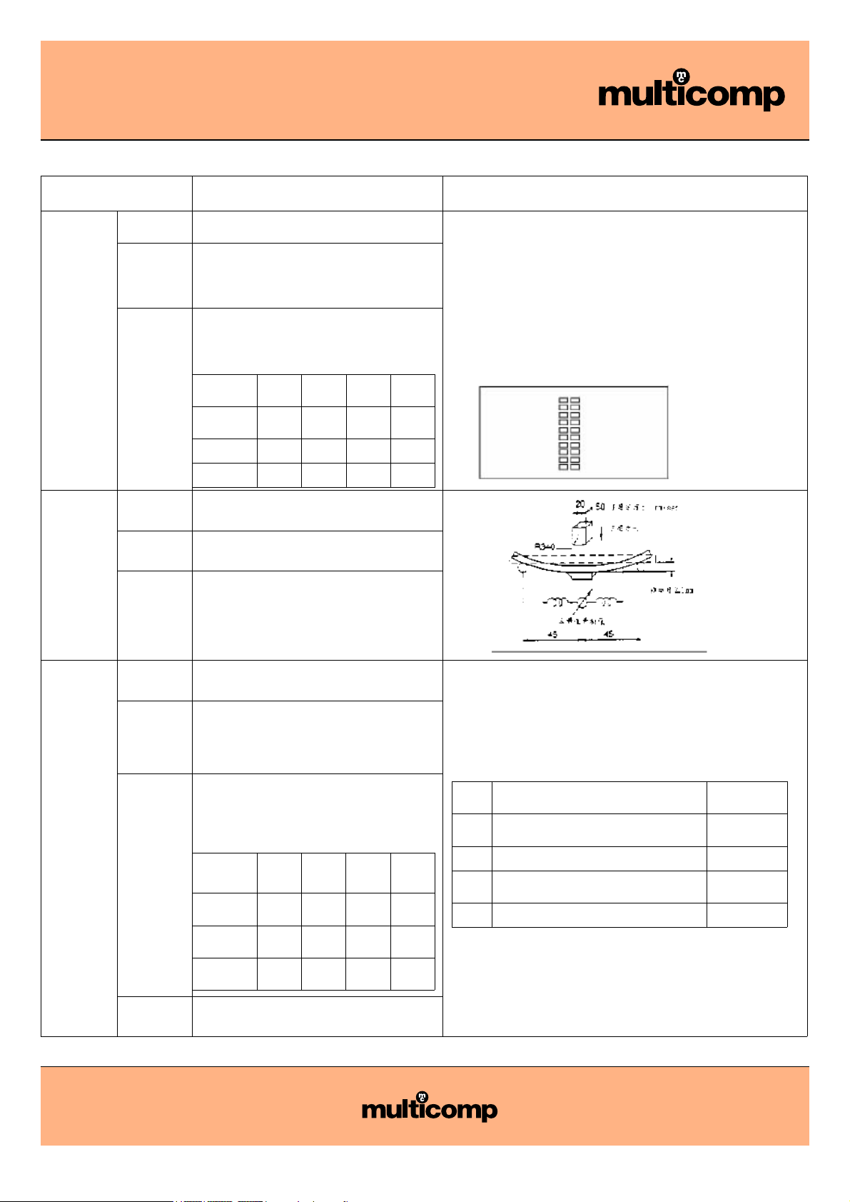
Solder the capacitors to the test jig as shown in figure below
with IR-Reflow method. The capacitor shall be subjected to a
simple harmonic motion with the entire frequency range, from
10 to 55 Hz and return to 10 Hz ,shall be transverse in 1 min.
Amplitude (total excursion): 1.5mm
Amplitude tolerance: ± 15%
This motion shall be applied for a period of 2
hours in each of 3 mutually perpendicular
directions (a total of 6 hours)
Capacitance
Change
(∆ C/C)
NPO: ±2.5% or ±0.25 pF maximum
(Whichever is larger)
X7R/X5R: ±7.5%
Y5V, Z5U: ±20%
DF or Q
NPO: C ≥30pF : Q ≥ 1000
C<30pF:Q ≥ 400 + 20°C
PS: C : Nominal capacitance (pF)
X7R, X5R, Y5V, Z5U : (Maximum Value)
Deflection
External
Appearance
No mechanical Damage
Bending
Strength
Flexure ≥ 1mm
Capacitance
Change
(∆ C/C)
NPO: ±5% or ±0.5 pF maximum
(Whichever is larger)
X7R/X5R: ±12.5%
Y5V: ±30%
Temperature
Cycle
External
Appearance
No mechanical Damage
(Not apply for 0402 product)
The capacitor shall be subject 5 cycles according to four heat
treatments listed in the following table.
Then leave the capacitors in ambient condition for the
following time before measurement.
Class II: 2~24 hours
Preconditioning: (only for class 2):
Perform a heat treatment at 150+0-10°C for one hour and
then let sit for 24 ±2 hours at room temperature.
Perform initial measurement.
Capacitance
Change
(∆ C/C)
NPO: ±2.5% or ±0.25 pF maximum
(Whichever is larger)
X7R/X5R: ±7.5%
Y5V: ±20%
DF NPO: C ≥30pF : Q ≥ 1000
C<30pF: Q ≥ 400 + 20°C
X7R, X5R, Y5V and Z5U (Maximum value)
IR
1000MΩ minimum or 50Ω *F
(Whichever is smaller)
T.C.
≥≥
50V
25V 16V
≤≤
10V
X7R/
X5R
2.5% 3.0% 3.5% 5.0%
Z5U 4.0% - - -
Y5V 5.0% 7.5% 9.0% 12.5%
T.C.
≥≥
50V
25V 16V
≤≤
10V
X7R/
X5R
2.5% 3.0% 3.5% 5.0%
Z5U 4.0% - - -
Y5V 5.0% 7.5% 9.0% 12.5%
Step Temperature (°C)
Duration
(Minutes)
1 Minimum Operation Temperature ±3 30 ±3
2 Room Temperature (25°C) 2 ~ 5
3 Minimum Operation Temperature ±3 30 ±3
4 Room Temperature (25°C) 2 ~ 5
Page 8
Nickel Barrier
Multilayer Ceramic Capacitors
Page 8 27/04/06 V1.0
Precaution For Handling
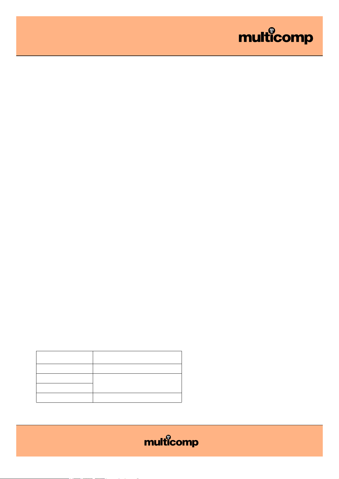
The multi-layer ceramic chip capacitors, may fall in a short circuit mode or in an open-circuit mode when subjected to severe
conditions of electrical, environmental and/or mechanical stress beyond the specified “Ratings” and specified “Condition” in the
Catalog and the Specifications, resulting in burnout, flaming or glowing in the worst case. So some common sense of application by
customer is necessary. Here the following article are some key points that need to take attention in application for customer reference
only:
Operating Conditions and Circuit Design
Operating temperature range
The specified “Operating Temperature Range” in the catalog is absolute maximum and minimum temperature rating. So in any case,
each the Capacitor shall be operated within the specified “Operating Temperature Range”.
Design of Voltage applications
The capacitors shall not be operated exceeding the specified “Rated Voltage” in the catalog. If voltage ratings are exceeded the
Capacitors could result in failure of damage. In case of application of DC and AC voltage to the capacitors, the designed peak voltage
shall be within the specified “Rated Voltage”.
Charging and Discharging Current
The capacitors shall not be operated beyond the specified “Maximum Charging / Discharging Current Rated” in the specification,
Application to a low impedance circuit such as a “secondary power circuit” are not recommended for safety.
Temperature Rise by Dielectric Loss of the capacitor
The “Operating Temperature Range” mentioned above shall include a maximum surface temperature rise of 20°C, which is caused by
the Dielectric loss of the Capacitor and applied electrical stress (such as voltage, frequency and wave form etc.)
It is recommended to measure and check “Surface temperature of the Capacitor” in your equipment at your estimated / designed
maximum ambient temperature.
Restriction on Environmental Conditions
The Capacitors shall not be operated and / or stored under following environmental conditions:
(a) To be exposed directly to water or salt water.
(b) To be exposed directly to sunlight.
(c) Under conditions of dew formation.
(d) Under conditions of corrosive atmosphere such as hydrogen sulfas, sulphurous acid, chlorine, or ammonia etc.
(e) Under severe condition of vibrations or shock beyond the specified conditions in the Specifications.
Secular change in Capacitance
(1) Peculiar characteristics of “Secular Changes in Capacitance” are observed in the Capacitors (Class 2 High Dielectric Constant
Temperature Characteristics “X7R” and “Y5V”. The “secular change” shall be considered in your circuit design.
(2) The Capacitance change, due to the individual characteristics of ceramic dielectric materials applied, can be recovered to the
each initial values at shipping by a heat treatment (140 to 150°C for 1 hour).
Design of Printed Circuit Board
Selection of Printed Circuit Boards
When the Capacitors are mounted and soldered on an “Aluminium’s Substrate has influences on Capacitor’s reliability against
“Temperatures Cycles” and “Heat shock” because of difference of thermal expansion dose not deterioration the characteristics of the
Capacitors.
There are some thermal expansion factor for different kink of PC board material as follows
PC Board Material Thermal Expansion Factor (mm/°C)
Glass Epoxy
1.4 x 10
-5
Paper Phenol
2.2 x 10
-5
Composite
Alumina
6.5 x 10
-6
Page 9
Nickel Barrier
Multilayer Ceramic Capacitors
Page 9 27/04/06 V1.0
Design of Land Pattern
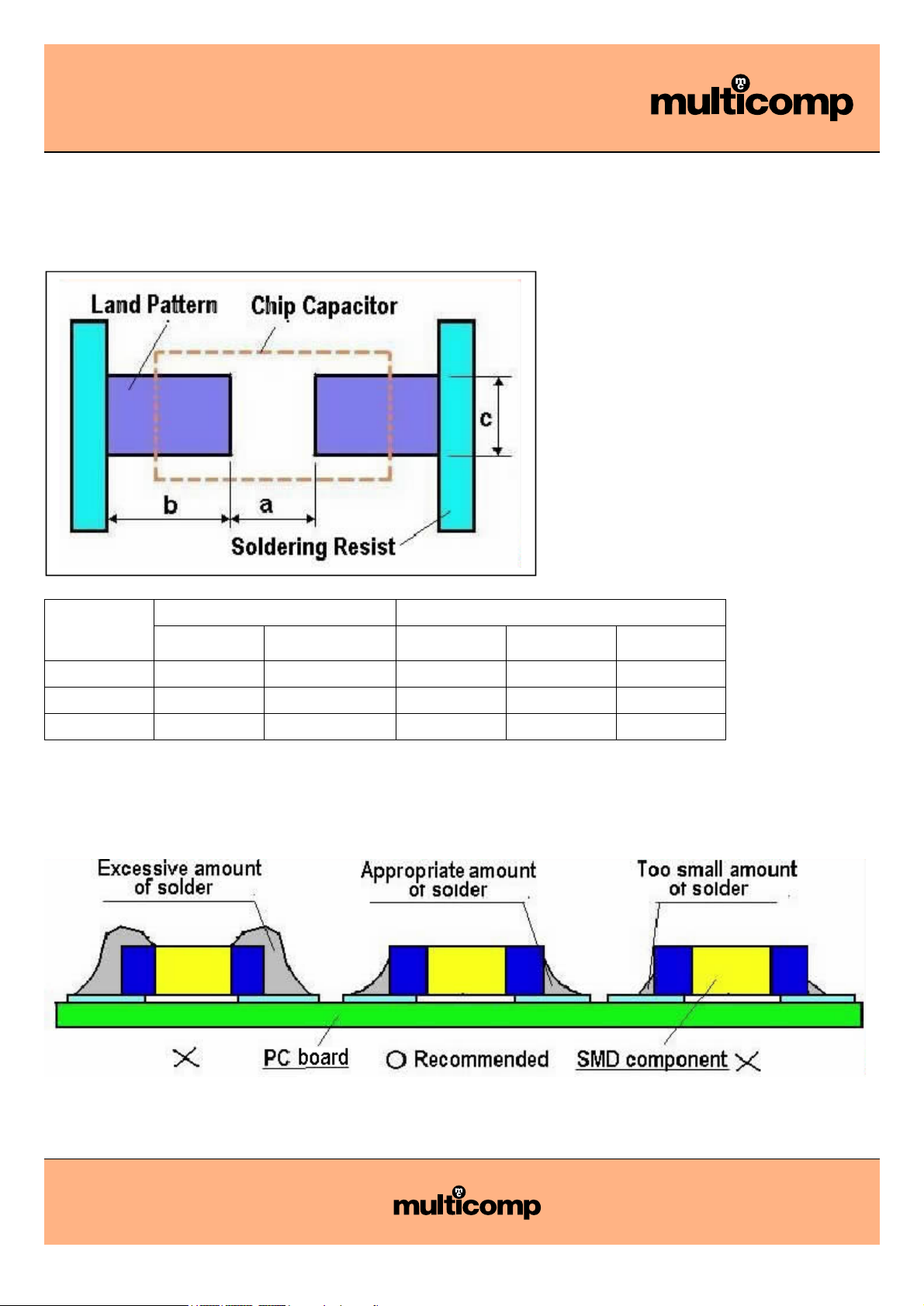
Recommended Dimensions of Lands. As shown in Table 1 and Figure 1.
Note: * Too large land required excess amount of solder.
** The Dimensions shall be symmetrical.
Figure 1 Recommended Land Dimensions:
Size
Chip Dimensions Land Dimension
Length
(L)
Width
(W)
a b c
0603 1.6 0.8 0.70 ~ 1.00 0.80 ~ 1.00 0.60 ~ 0.80
0805 2.0 1.25 1.00 ~ 1.30 1.00 ~ 1.20 0.80 ~ 1.10
1206 3.2 1.6 2.10 ~ 2.50 1.10 ~ 1.30 1.10 ~ 1.30
Recommend amount of solder:
Recommended amount of solder: As shown in Figure2. Excess amount of solder gives large mechanical stresses to the capacitors /
Components.
Figure 2: Recommended amount of solder
Table 1
Dimensions: Millimetres
Page 10
Nickel Barrier
Multilayer Ceramic Capacitors
Page 10 27/04/06 V1.0
Component Layout
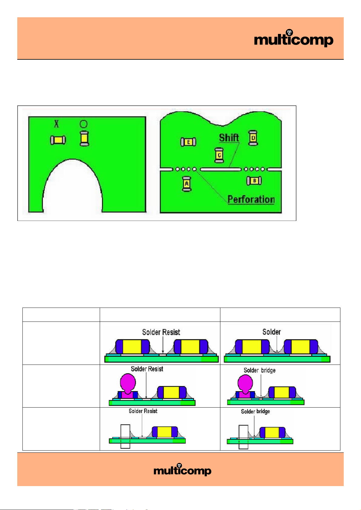
When placing / mounting the capacitors / components near an area which is apt to bend or a grid groove on the PC board. It is
advisable to have both electrodes subjected to uniform stresses, or to position the component electrodes at right angles to the grid
groove or bending line.
Figure 3 Component Layout
Uneven mounting density
O: Proper X: Improper
Probability at which the chip capacitor is broken by the stress on PC board break
A > B = C >D > E
Mounting Density and Spaces
Placements in too narrow spaces between components may cause “ Solder Bridges” during soldering. The minimum space between
components shall be 0.5mm in view of the positioning tolerances of the mounting machines and the dimensional tolerances of the
components and PC boards.
Applications of Solder Resist
Application of Solder Resist are effective to prevent solder bridges and to control amounts of solder on PC boards ( As shown in
Table 2).
Recommended Application Examples Examples of Solder Bridges
Narrow Spacing
between Chip
Components
Radial Components
are directly
connected to
Chip Components
Common lands are
close to Chip
Components
Page 11
Nickel Barrier
Multilayer Ceramic Capacitors
Page 11 27/04/06 V1.0
Precautions for Assembly
Adhesives for Mounting
(1) Selection of adhesives
a. The viscosity of an adhesive for mountings shall be such that the adhesive dose not flow off on the land during its curing.
b. If the adhesive is too low in its viscosity, mounted components may be out of alignment after or during soldering.
c. The adhesives shall not be corrosive or chemically active to the mounted components and the PC boards.
d. The amount of adhesive shall be such that the adhesive does not flow off or be out of alignment.
e. Adhesives for mountings can be cured by ultraviolet or infrared radiation. In order to prevent the terminal electrodes of the
Capacitors the curing shall be done at conditions of 180°C maximum, for 2 minutes maximum.
Chip Mounting consideration
In mounting the Capacitors / components on a printed circuit board, any bending and expanding force against them shall be kept
minimum to prevent them from being damaged or cracked.
Following precautions and recommendation shall be observed carefully in the process:
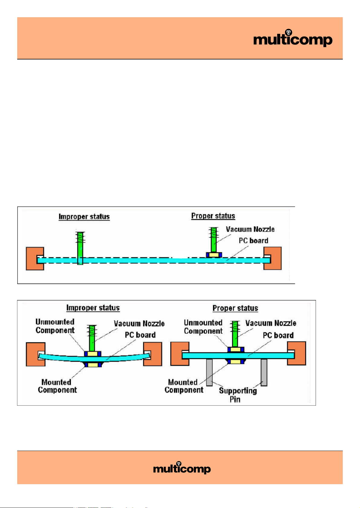
(1) Maximum stroke of the vacuum nozzle shall be adjusted so that the pushing force to the printed circuit board shall be limited to a
static of 1 to 3 N (100 to 300 gf) (See Figure4).
(2) Maximum stroke of the nozzle shall be adjusted so that the maximum bending of printed circuit board dose not exceeded 0.5mm
(See Figure 4)
Figure 4
(3) The printed circuit board shall be supported by means of adequate supporting pins as shown in Fig.5-(b)
Figure 5
Page 12
Nickel Barrier
Multilayer Ceramic Capacitors
Page 12 27/04/06 V1.0
Soldering Flux and Solder
(1) Solder Flux:
a. The content of halogen in the soldering shall be 0.2 wt% or less.
b. Rosin-based and non-activated soldering flux is recommended.
(2) Water soluble type Soldering Flux:
In case of water soluble type soldering flux being applied, the flux residue on the surface of PC boards may have influences on the
reliability of the components and cause deterioration and failures of them.
(3) Solder:
An eutectic solder (Sn63:Pb37) is recommended.
Soldering
Since a multilayer ceramic chip capacitor comes into direct contact with melted solder during soldering. It is exposed to potentially
damaging mechanical stress caused by the sudden temperature change. The capacitor may also be subject to silver migration, and
to contamination by the flux. Because of these factors, soldering technique is critical. Adhere to the following guidelines.
Hand soldering
In hand soldering of the Capacitors, large temperature gradient between preheated the capacitors and the tip of soldering iron may
cause electrical failures and mechanical damages such as cracking of breaking of the devices. The soldering shall be carefully
controlled and carried out so that the temperature gradient is kept minimum with following recommended
conditions for hand soldering.
Recommended Soldering Conditions:
(1) Solder:
φ1mm Thread eutectic solder (Sn63:Pb37) with soldering flux *in the core.
*Rosin-based, and mom-activated flux is recommended.
(2) Preheating:
The capacitors shall be preheated so that “Temperature Gradient” between the devices and the tip of soldering iron is 150°C or
below.
(3) Soldering iron:
Rated Power of 20W Max with 3mm soldering tip in diameter.
Temperature of soldering iron tip: 300°C maximum.
(The required amount of solder shall be melted in advance on the soldering tip.)
(4)Cooling:
After soldering, the Capacitors shall cooled gradually at room ambient temperature.
Flow Soldering
In flow soldering process, abnormal and thermal and mechanical stresses, caused by “Temperature Gradient” between the mounted
Capacitors, resulting in failures and damages of the capacitors. So it is essential that the soldering process shall controlled to the
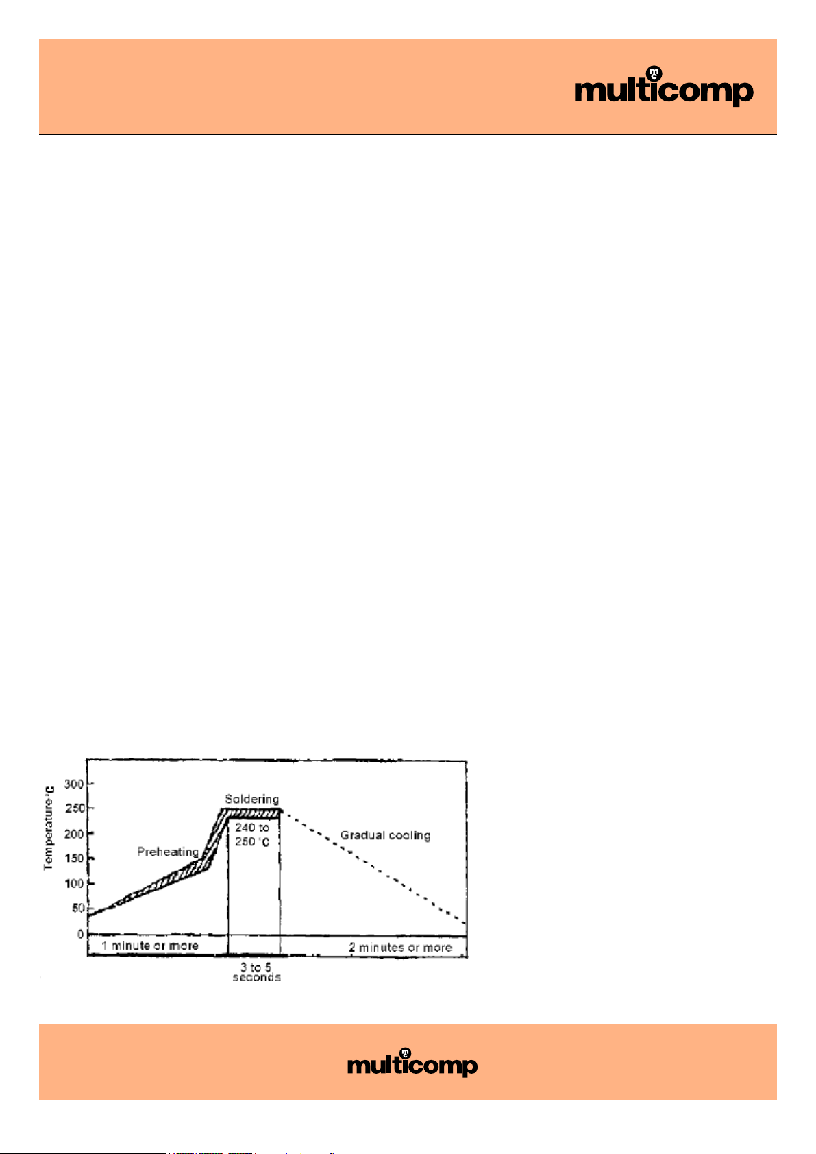
following recommended conditions and precautions. (See Figure 6)
Figure 6 Recommended Soldering Temperature Time Profile (Flow soldering)
Page 13
Nickel Barrier
Multilayer Ceramic Capacitors
Page 13 27/04/06 V1.0
(1) Application of Flux:
The soldering flux(3.3) shall applied to the mounted Capacitors thinly and uniformly by forming method.
(2) Preheating:
The mounted Capacitors / Components shall be preheated sufficiently so that the “ Temperature Gradient” between the Capacitors /
Components and the melted solder shall be 150°C or below.
(3) Immersion to Soldering Bath:
The Capacitors shall be immersed into a soldering bath of 240 to 250°C for 3 to 5 seconds.
(4)Cooling:
The Capacitors shall be cooled gradually to room ambient temperature with the cooling temperature rates of 8°C/s maximum from
250°C to 170°C and 4°C/s maximum from 170°C to 130°C.
(5) Flux Cleaning:
When the Capacitors are immersed into cleaning solvent, it shall be confirmed that the surface temperature of devices do not exceed
100°C (See 3.5).
Reflow soldering.
I n reflow soldering process, the mounted Capacitors / Components are generally heated and Soldering by a thermal conduction
system such as an “Infrared radiation and hot blast soldering system” or a “Vapour Phase Soldering System (VPS)”, Large
temperature gradients such as a rapid heating and cooling in the process may cause electrical and mechanical damages if the
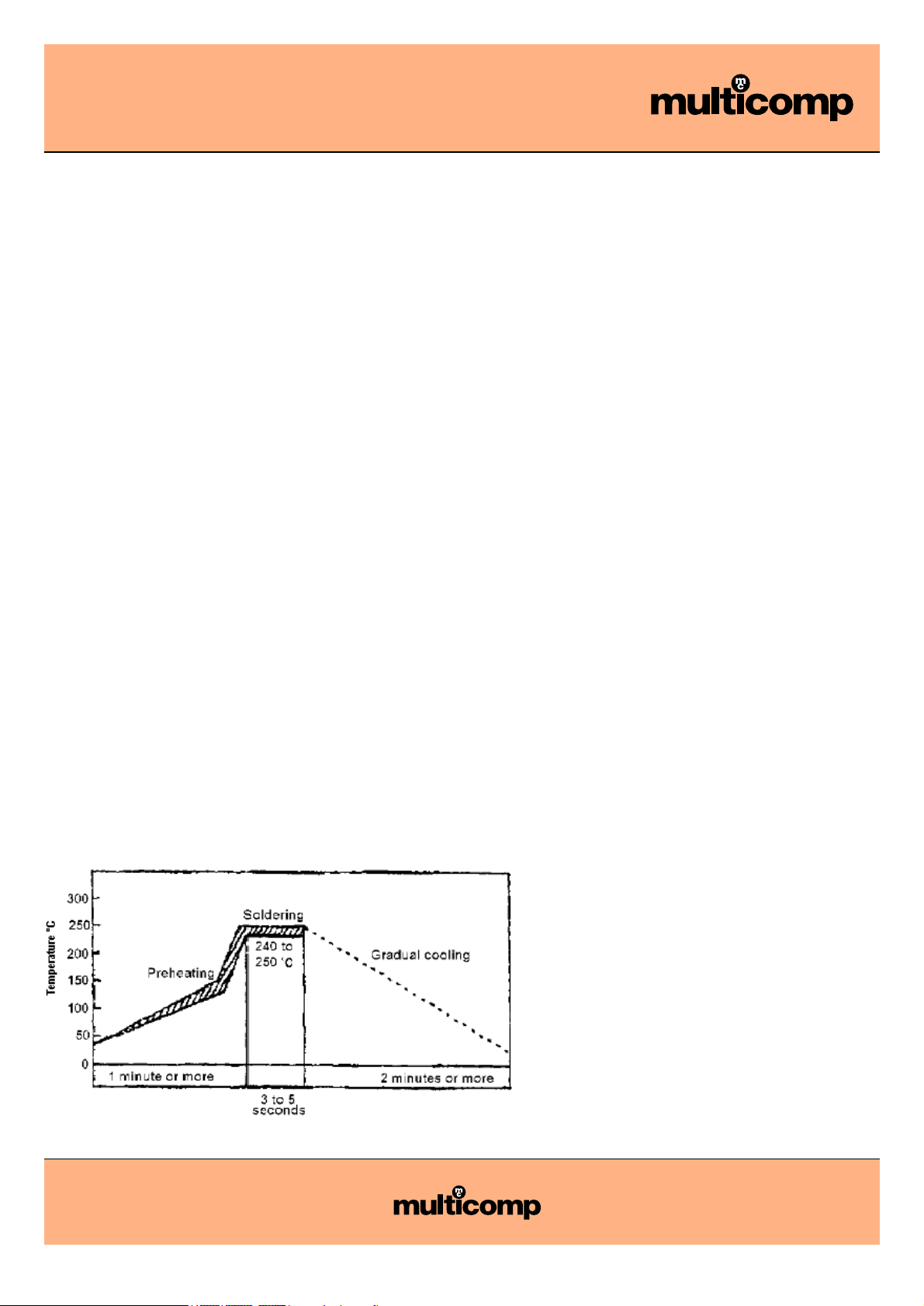
device. It is essential that the soldering process shall be controlled by following recommended conditions and precaution. (See
Figure7)
For Tin-Lead (Sn/Pb) Termination component:
(1) Preheating 1.
The mounted Capacitors / Components shall be preheated sufficiently, for 60 to 90 seconds so that the surface temperature of them
to be 140 to 150°C.
(2) Preheating 2.
After “Preheating 1”, the mounted Capacitors / Components shall be the elevated temperature of 150 to 200°C for 2 to 6 Seconds.
(3) Soldering:
The mounted Capacitors / Components shall be heated under the specified heating conditions (200 to 240 to 200°C for total 20 to 40
seconds, See Figure7 ) and shall be soldered at the maximum temperature of 240°C for 10 seconds of less.
(4)Cooling:
After the soldering, the mounted Capacitors / Components shall be gradually cooled to room ambient temperature for preventing
mechanical damages such as cracking of the devices.
(5) Flux Cleaning:
When the mounted Capacitors / Components are immersed into cleaning solvent, it shall be confirmed the surfaces temperatures of
them do not exceeding 100°C.
Note: If the mounted Capacitors / Components are partially heated in the soldering process, the devices may be separated form the
printed circuit board by the surface tension of partially melted solder, and stand up like a “Tomb Stone”.
Figure 7 Recommended Soldering Temperature Time Profile for Tin-Lead component (Reflow Soldering)
Page 14
Nickel Barrier
Multilayer Ceramic Capacitors
Page 14 27/04/06 V1.0
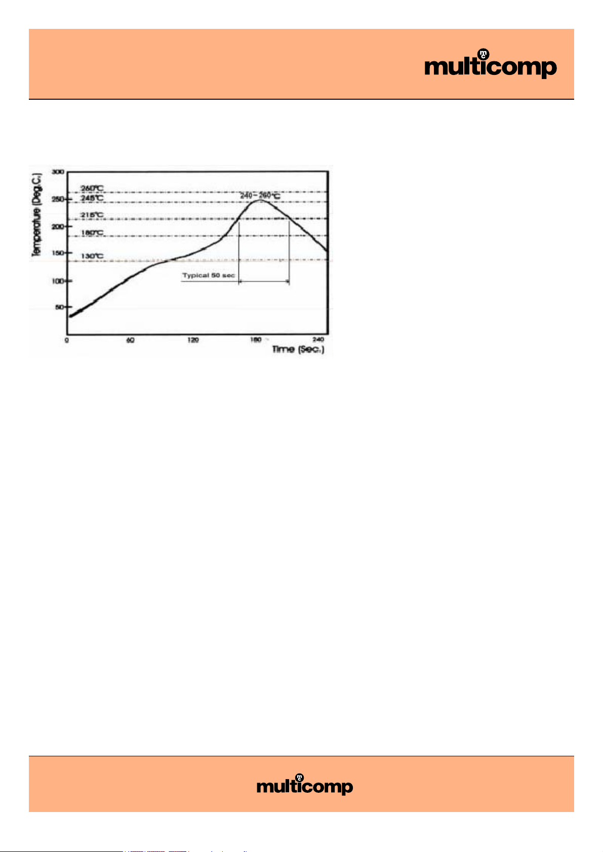
For Lead-free (Pure Tin plating termination) Termination component
Essentially, the soldering temperature for Lead-free component is a little higher than that for Tin-Lead component, but need to take
consideration of the thermal effect for all other components mounting on board at the same time. The below picture is a
recommended soldering profile for Lead-free component
Figure 8 Recommended Soldering Temperature Time Profile for Lead-free component (Reflow Soldering)
Post soldering Cleaning
(1)Residues of corrosive soldering fluxes on the PC board after cleaning may greatly have influences on the electrical characteristics
and the reliability, (such as humidity resistance) of the Capacitors, which have been mounted on the board. It shall be confirmed that
the characteristic and reliability at the devices are no effected by applied cleaning conditions.
(2) Solubility of alternative cleaning solvent such as alcohol etc., is inferior to that of Freon cleaning solvent in the flux cleaning. So in
case of alternative cleaning solvents, fresh cleaning solvent shall be used, and sufficient rinsing and drying shall carried out.
(3) When an ultrasonic cleaning is applied to the mounted Capacitors on PC board, following conditions energy and the
recommended for preventing failures or damages of the devices due to the large vibration energy and the resonant caused by the
ultrasonic waves.
Frequency :29KHz maximum.
Radiated Power :20 W/litre maximum.
Period :5 minutes maximum.
Process Inspection
When the mounted printed circuit are inspected with measuring terminal pins, abnormal and excess mechanical stresses shall not be
applied to the PC board mounted components, to prevent failure or damages of the devices.
(1) The mounted PC board shall be supported a same adequate supporting pins prevent their banding.
(2) It shall be confirmed that the measuring pin have the right tip in shape, equal in height and are set in the tight positions.
(3) The amount of adhesive shall be such that the adhesive dose flow off or be out of alignment.
Protective Coating
When the surface of a printed board on which the Capacitors has been mounted is coated with Resin to protect against moisture and
dust, it shall be confirmed that the protective coat dose not have influences on reliability of the capacitors in the actual equipment.
(1) Coating materials, such as being corrosive and chemically active, shall not be applied to the capacitors and other components.
(2) Coating materials with a large expansively shall not be applied to the Capacitors for preventing failures or damages (such as
cracking) of the devices in the curing process.
Page 15
Nickel Barrier
Multilayer Ceramic Capacitors
Page 15 27/04/06 V1.0
Dividing / Breaking of PC Boards
(1) Abnormal and excessive mechanical stresses, such as bending or expanding force on the components on the printed circuit
board, shall be kept minimum in the dividing / breaking.
(2) Dividing / Breaking of the PC board shall be done carefully at moderate speed using a Jig boards from mechanical damages.
Long Term Storage
The Capacitors shall not be stored under severe conditions of high temperatures and high humidity. Store them under 40°C
maximum and 75%RH maximum Use them within 6 months and check the solderability before use.
Part Number Table
Type Voltage (V) Temperature Characteristics Code Part Number
0603
10 F
N0603F474ZCT
N0603F474ZNT
16
R
B0603R104KCT
B0603R104KNT
25
T0603R223KCT
T0603R473KCT
T0603R223KNT
T0603R473KNT
F
T0603F104ZCT
T0603F104ZNT
50
C
U0603C220JCT
U0603C101JCT
U0603C221JCT
U0603C102JCT
U0603C100JNT
U0603C220JNT
U0603C470JNT
U0603C101JNT
U0603C221JNT
U0603C331JNT
U0603C471JNT
U0603C102JNT
R
U0603R102KCT
U0603R103KCT
U0603R471KNT
U0603R102KNT
U0603R222KNT
U0603R332KNT
U0603R472KNT
U0603R103KNT
F
U0603F103ZNT
U0603F473ZNT
Page 16
Nickel Barrier
Multilayer Ceramic Capacitors
Page 16 27/04/06 V1.0
Part Number Table
Type Voltage (V) Temperature Characteristics Code Part Number
0805
10
R
N0805R105KCT
N0805R105KNT
16
B0805R224KCT
B0805R334KCT
B0805R474KCT
B0805R224KNT
B0805R334KNT
B0805R474KNT
25 F
T0805F105ZCT
T0805F105ZNT
50
C
U0805C102JCT
U0805C222JCT
U0805C102JNT
U0805C222JNT
R
U0805R102KCT
U0805R103KCT
U0805R223KCT
U0805R473KCT
U0805R104KCT
U0805R102KNT
U0805R222KNT
U0805R472KNT
U0805R103KNT
U0805R223KNT
U0805R473KNT
U0805R104KNT
F
U0805F104ZCT
U0805F104ZNT
100 C
A0805C100JCT
A0805C220JCT
A0805C330JCT
A0805C470JCT
A0805C101JCT
A0805C221JCT
A0805C471JCT
A0805C100JNT
A0805C220JNT
A0805C330JNT
Page 17
Nickel Barrier
Multilayer Ceramic Capacitors
Page 17 27/04/06 V1.0
Part Number Table
Type Voltage (V) Temperature Characteristics Code Part Number
0805 100 C
A0805C470JNT
A0805C101JNT
A0805C221JNT
A0805C331JNT
A0805C471JNT
1206
10
R
N1206R225KCT
N1206R225KNT
16
B1206R105KCT
B1206R105KNT
F
B1206F225ZCT
B1206F225ZNT
25
C
T1206C472JCT
T1206C103JCT
T1206C472JNT
T1206C103JNT
R
T1206R334KCT
T1206R474KCT
T1206R334KNT
T1206R474KNT
50
U1206R103KCT
U1206R104KCT
U1206R102KNT
U1206R222KNT
U1206R332KNT
U1206R472KNT
U1206R103KNT
U1206R223KNT
U1206R333KNT
U1206R473KNT
U1206R104KNT
F
B1206F475ZCT
B1206F475ZNT
100 C
A1206C100JCT
A1206C220JCT
A1206C101JCT
A1206C221JCT
A1206C331JCT
Page 18
Nickel Barrier
Multilayer Ceramic Capacitors
Page 18 27/04/06 V1.0
Part Number Table
Type Voltage (V) Temperature Characteristics Code Part Number
1206 100 C
A1206C471JCT
A1206C102JCT
A1206C100JNT
A1206C220JNT
A1206C330JNT
A1206C470JNT
A1206C101JNT
A1206C221JNT
A1206C331JNT
A1206C471JNT
A1206C102JNT
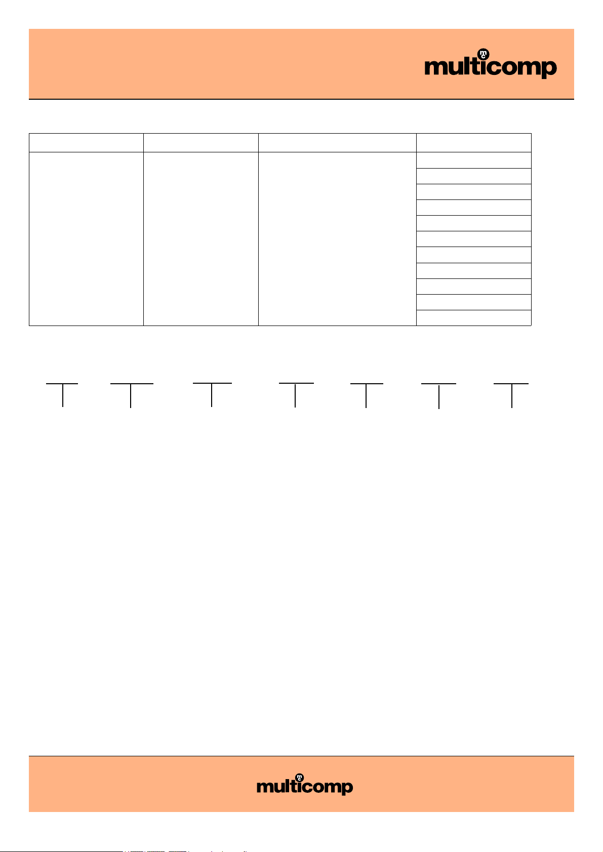
Part Number Explanation
U 0805 C 102
J N T
Rated
Voltage
Part
Dimension
Temperature
Characteristics
Code
Capacitance
Code
Tolerance
Code
Termination
Code
Packaging
Code
Rated Voltage : A, B, T and U.
Part Dimension : 0603, 0805 and 1206.
Temperature Characteristics Code : C, R and F.
Capacitance Code : 100, 101, 102, 103 and 472.
Tolerance Code : J, K and Z.
Termination Code : Termination Type.
Packaging Code : Packaging Type.
Page 19

For enquiries from all other markets
Nickel Barrier
Multilayer Ceramic Capacitors
Page 19 27/04/06 V1.0
Notes:
International Sales Offices:
AUSTRALIA – Farnell InOne
Tel No: ++ 61 2 9645 8888
Fax No: ++ 61 2 9644 7898
FRANCE – Farnell InOne
Tel No: ++ 33 474 68 99 99
Fax No: ++ 33 474 68 99 90
NORWAY
– Farnell InOne
Tel No: ++ 45 44 53 66 66
Fax No: ++ 45 44 53 66 02
AUSTRIA – Farnell InOne
Tel No: ++ 43 662 2180 680
Fax No: ++ 43 662 2180 670
GERMANY – Farnell InOne
Tel No: ++ 49 89 61 39 39 39
Fax No: ++ 49 89 613 59 01
PORTUGAL – Farnell InOne
Tel No: ++ 34 93 475 8804
Fax No: ++ 34 93 474 5288
ESTONIA
– Farnell InOne
Tel No: ++ 358 9 560 7780
Fax No: ++ 358 9 345 5411
NETHERLANDS
– Farnell InOne
Tel No: ++ 31 30 241 7373
Fax No: ++ 31 30 241 7333
UK – Farnell InOne
Tel No: ++ 44 8701 200 200
Fax No: ++ 44 8701 200 201
SINGAPORE
–
Farnell-Newark InOne
Tel No: ++ 65 6788 0200
Fax No: ++ 65 6788 0300
HONG KONG
–
Farnell-Newark InOne
Tel No: ++ 852 2268 9888
Fax No: ++ 852 2268 9899
BELGIUM – Farnell InOne
Tel No: ++ 32 3 475 2810
Fax No: ++ 32 3 227 3648
BRAZIL – Farnell-Newark InOne
Tel No: ++ 55 11 4066 9400
Fax No: ++ 55 11 4066 9410
IRELAND – Farnell InOne
Tel No: ++ 353 1 830 9277
Fax No: ++ 353 1 830 9016
SPAIN – Farnell InOne
Tel No: ++ 34 93 475 8805
Fax No: ++ 34 93 474 5107
CHINA – Farnell-Newark InOne
Tel No: ++86 10 6238 5152
Fax No: ++86 10 6238 5022
ITALY – Farnell InOne
Tel No: ++ 39 02 93 995 200
Fax No: ++ 39 02 93 995 300
SWEDEN – Farnell InOne
Tel No: ++ 46 8 730 50 00
Fax No: ++ 46 8 83 52 62
MALAYSIA –
Farnell-Newark InOne
Tel No: ++ 60 3 7873 8000
Fax No: ++ 60 3 7873 7000
SWITZERLAND
– Farnell InOne
Tel No: ++ 41 1 204 64 64
Fax No: ++ 41 1 204 64 54
DENMARK – Farnell InOne
Tel No: ++ 45 44 53 66 44
Fax No: ++ 45 44 53 66 06
UK – CPC
++ 44 8701 202 530
++ 44 8701 202 531
UK – BuckHickman InOne
++ 44 8450 510 150
++ 44 8450 510 130
NEW ZEALAND
– Farnell InOne
Tel No: ++ 64 9 357 0646
Fax No: ++ 64 9 357 0656
EXPORT
– Farnell InOne
Tel No: ++ 44 8701 200 208
Fax No: ++ 44 8701 200 209
export
FINLAND – Farnell InOne
Tel No: ++ 358 9 560 7780
Fax No: ++ 358 9 345 5411
Disclaimer This data sheet and its contents (the "Information") belong to the Premier Farnell Group (the "Group") or are licensed to it. No licence is granted for the use of it other than for information purposes
in connection with the products to which it relates. No licence of any intellectual property rights is granted. The Information is subject to change without notice and replaces all data sheets previously supplied.
The Information supplied is believed to be accurate but the Group assumes no responsibility for its accuracy or completeness, any error in or omission from it or for any use made of it. Users of this data
sheet should check for themselves the Information and the suitability of the products for their purpose and not make any assumptions based on information included or omitted. Liability for loss or damage
resulting from any reliance on the Information or use of it (including liability resulting from negligence or where the Group was aware of the possibility of such loss or damage arising) is excluded.
This will not operate to limit or restrict the Group's liability for death or personal injury resulting from its negligence. Multicomp is the registered trademark of the Group. © Premier Farnell plc 2004.
http://www.farnellinone.com
http://www.buckhickmaninone.com
http://www.cpc.co.uk
 Loading...