

Page 1
Philips Semiconductors Product specification
NE8392CCoaxial transceiver interface for Ethernet/Thin Ethernet
1
1995 May 1 853-1693 15180
DESCRIPTION
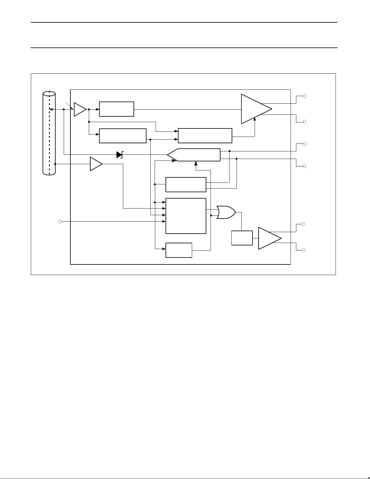
The NE8392C Coaxial Transceiver Interface (CTI) is a bipolar
coaxial line driver/receiver for Ethernet (10base5) and Thin Ethernet
(10base2) local area networks. The CTI is connected between the
coaxial cable and the Data Terminal Equipment (DTE) and consists
of a receiver, transmitter, receive-mode collision detector, heartbeat
generator and jabber timer (see Block Diagram). The transmitter
output connects directly to a doubly terminated 50Ω cable, while the
receiver output, collision detector output and transmitter input are
connected to the DTE through isolation transformers. Isolation
between the CTI and the DTE is an IEEE 802.3 requirement that
can be met on signal lines by using a set of pulse transformers
normally available in a standard 16-pin DIP. Power isolation for the
CTI is achieved using DC-to-DC conversion through a power
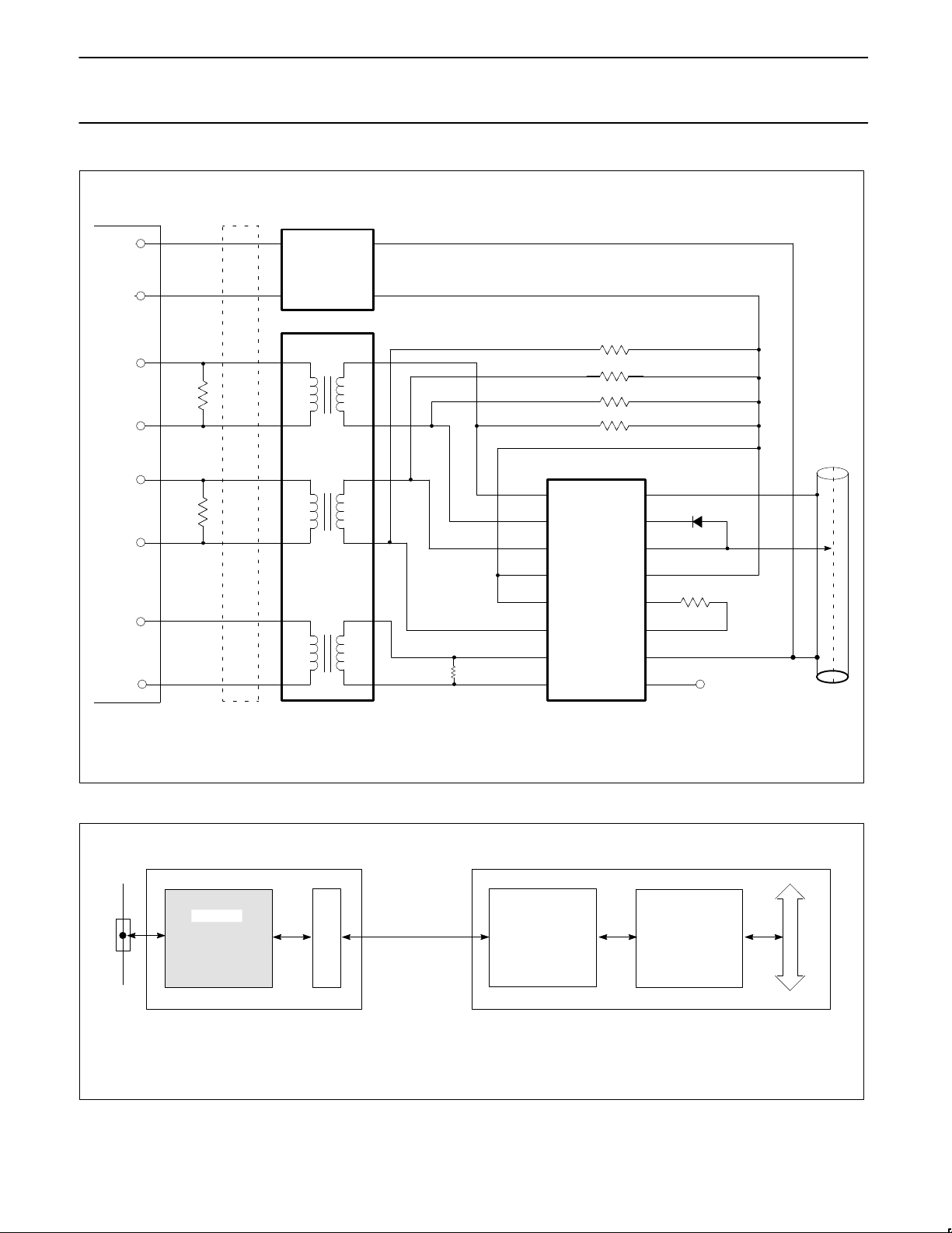
transformer (see Figure 1, Connection Diagram).
During transmission the jabber timer is initiated to disable the CTI
transmitter in the event of a longer than legal length data packet.
Receive-mode collision detection circuitry monitors the signals on
the coaxial cable to determine the presence of colliding packets and
signals the DTE in the event of a collision. At the end of every
transmission the heartbeat generator creates a pseudo collision for
a short time to ensure that the collision circuitry is functioning
correctly. The heartbeat function can be disabled for repeater
applications.
The CTI is normally part of a three chip set that implements a
complete Ethernet/ Thin Ethernet network interface for a DTE (see
Figure 2, Interface Diagram). The other chips are a Serial Network
Interface (SNI) and a Network Interface Controller (NIC). The SNI
provides Manchester Encoding and Decoding while the NIC handles
the media access protocol and buffer management tasks.
FEATURES
•Compatible with Ethernet II IEEE 802.3 10base5 and 10base2,
and ISO 8802/3 interface specifications
•100% drop-in compatible with industry standard 8392 sockets
•Integrates all transceiver electronics except signal and power
isolation
•Only one external resistor required for setting coaxial signaling
current
•Jabber timer function integrated on chip
•Heartbeat generator can be externally disabled for operation as
IEEE 802.3 compatible repeaters
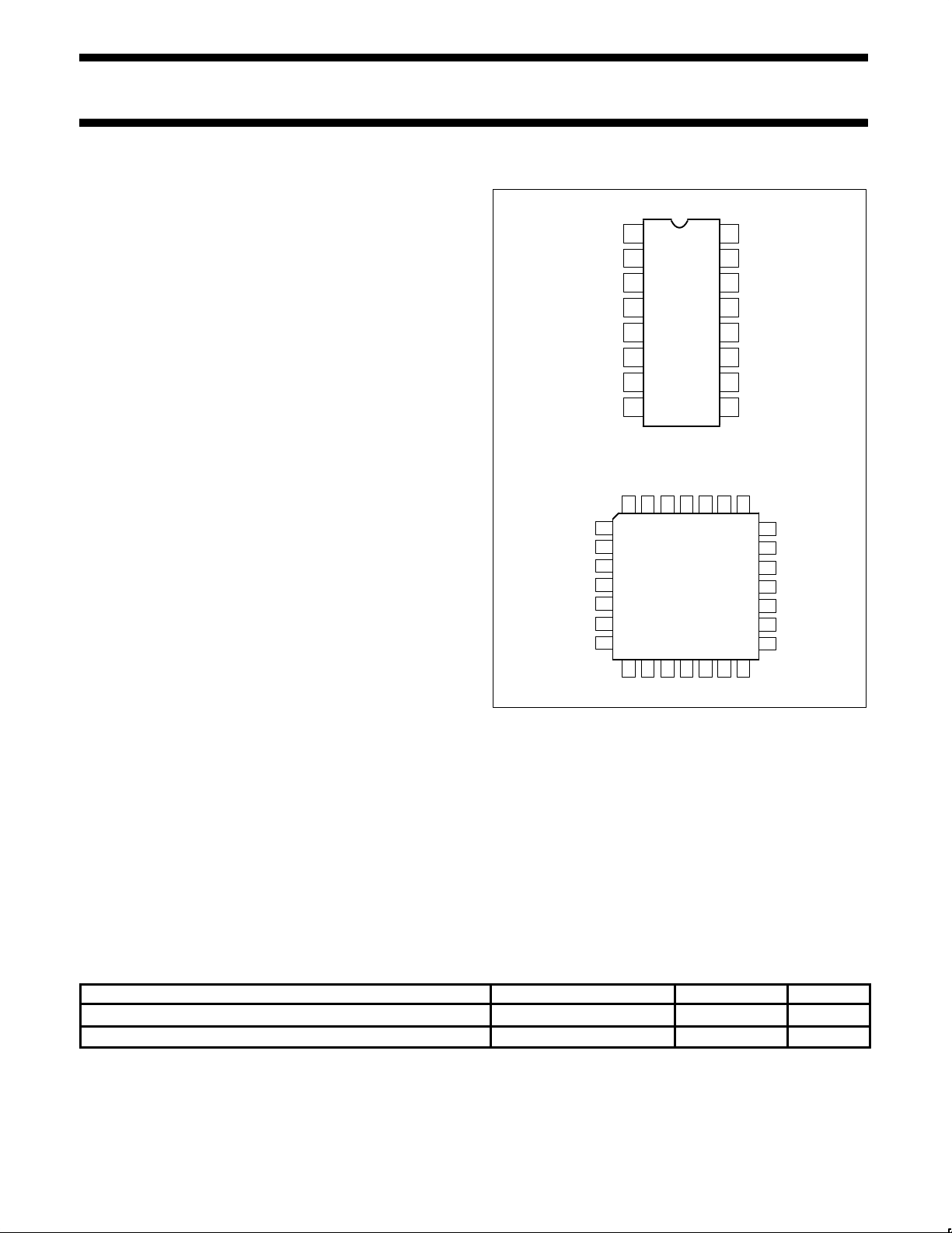
PIN CONFIGURATION
CD+ 1
CD– 2
RX+ 3
V
EE
4
V
EE
5
RX– 6
TX+ 7
TX– 8
16 CDS
15 TXO
14 RXI
13 V
EE
12 RR–
11 RR+
10 GND
9 HBE
N PACKAGE
1234
5
6
7
8
9
10
11
12 13 14 15 16 17 18
19
20
21
22
23
24
25
262728
V
EE
V
EE
V
EE
V
EE
V
EE
V
EE
V
EE
V
EE
V
EE
V
EE
V
EE
V
EE
V
EE
RR–
RX+
CD–
CD+
CDS
TXO
N/C
RXI
RX–
TX+
TX–
HBE
GND
GND
RR+
A PACKAGE
SD00283
•On-chip precision voltage reference for receive mode collision
detection
•Squelch circuitry on all signal inputs rejects noise
•Full ESD protection
•Standard 16-pin DIP and 28-pin PLCC packages
•Power-on reset prevents glitches on coaxial cable during power
up.
•Also available in advanced low-power BiCMOS technology. (See
selection chart and data sheets for the NE83C92, NE83Q92 or
NE83Q93 for appropriate optimal usages)
ORDERING INFORMATION
DESCRIPTION TEMPERATURE RANGE ORDER CODE DWG #
16-Pin Plastic Dual In-Line Package (DIP)
0 to +70°C
NE8392CN SOT28-4
28-Pin Plastic Lead Chip Carrier (PLCC)
0 to +70°C
NE8392CA SOT261-3
Page 2
Philips Semiconductors Product specification
NE8392CCoaxial transceiver interface for Ethernet/Thin Ethernet
1995 May 1
2
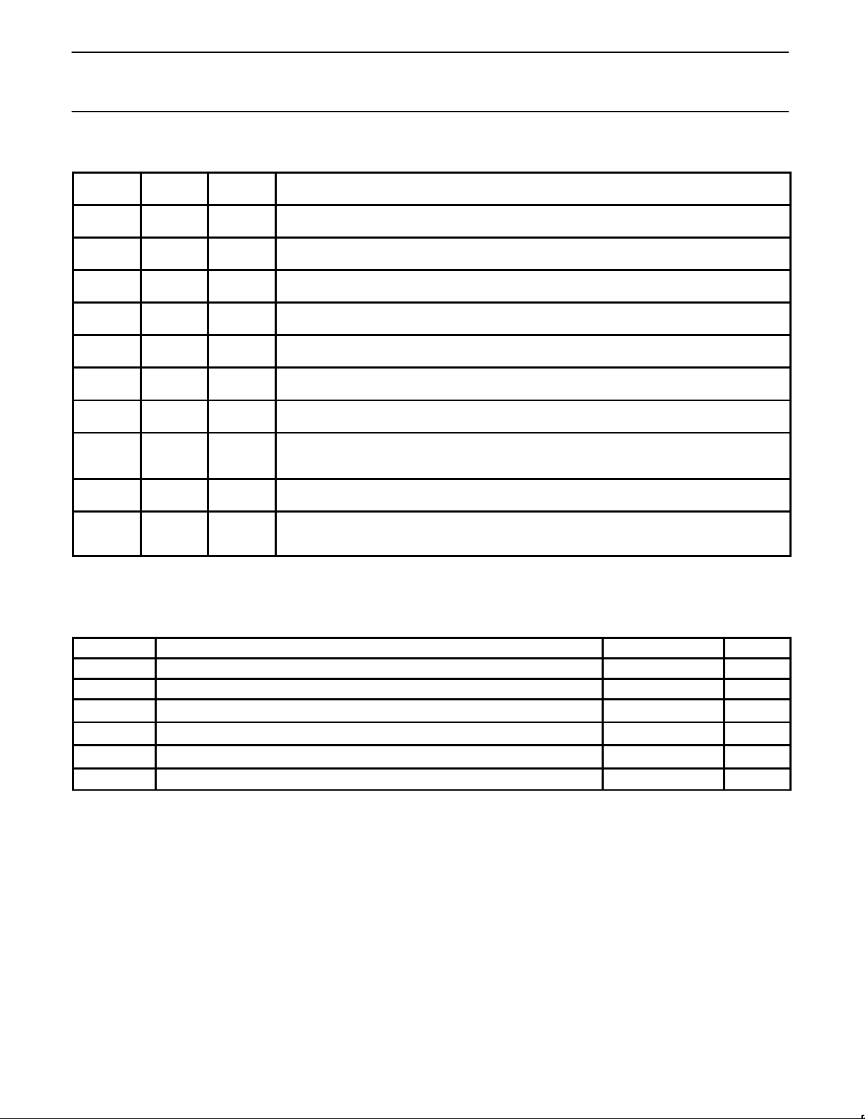
PIN DESCRIPTIONS
PIN NO.
N PKG
PIN NO.
PLCC
SYMBOL DESCRIPTION
1
2
2
3
CD+
CD–
Collision Outputs. Balanced differential line driver outputs which send a 10MHz oscillation signal to
the DTE in the event of a collision, jabber interrupt or heartbeat test.
3
6
4
12
RX+
RX–
Receiver Outputs. Balanced differential line driver outputs which send the received signal to the
DTE.
7
8
13
14
TX+
TX–
Transmitter Inputs. Balanced differential line receiver inputs which accept the transmission signal
from the DTE and apply it to the coaxial cable at TXO once it meets Tx squelch threshold.
9 15 HBE
Heartbeat Enable. The heartbeat function is disabled when this pin is connected to VEE and enabled
when connected to GND or left floating.
11
12
18
19
RR+
RR–
External Resistor. A 1kΩ (1%) resistor connected between these pins establishes the signaling
current at TXO. RR– is internally connected to V
EE
.
14 26 RXI
Receiver Input. This pin is connected directly to the coaxial cable. Received signals are equalized,
amplified, and sent to the DTE through the RX+ pins once it meets Rx squelch threshold.
15 28 TXO
Transmitter Output. This pin is connected directly (Thin Ethernet) or through an external isolating
diode (Ethernet) to the coaxial cable.
16 1 CDS
Collision Detect Sense. Ground sense connection for the collision detection circuitry. This pin
should be directly connected to the coaxial cable shield to prevent ground drops affecting the
collision threshold voltage.
10
16
17
GND Positive Supply Pin.
4
5
13
5 to 11
20 to 25
V
EE
Negative supply pins. These pins also serve as a low thermal resistance path for extracting heat
from the die. They should, therefore, be connected to a large metal area on the PC board.
NOTE:
1. The IEEE 802.3 name for CD is CI; for RX is DI; for TX is DO.
ABSOLUTE MAXIMUM RATINGS
SYMBOL PARAMETER RATING UNIT
V
EE
Supply voltage
1
–12 V
V
IN
Voltage at any input
1
0 to –12 V
T
STG
Storage temperature range –65 to +150
°C
T
SOLD
Lead soldering temperature (10sec.) +300
°C
T
J
Recommended max junction temperature
2
+130
°C
θ
JA
Thermal impedance (N and A packages) 60
°C/W
NOTE:
1. 100% measured in production.
2. The junction temperature is calculated from the following expression:
T
J
= TA + θ
JA
[VEE (0.08 + n x 0.05/100) + 8(VEE –2) / R]
where
T
A
= Ambient temperature in °C.
θ
JA
= Thermal resistance of package.
V
EE
= Normal operating supply voltage in volts.
n = Percentage transmitter duty cycle.
R = Pull down resistors on the RX and CD pins in Ω.
The N package is specially designed to have a low θ
JA
by directly connecting the four center Pins 4, 5, 12, and 13 to the die attachment area.
These four pins then provide a conductive heat flow path from the die to the PCB where they should be soldered to a large area V
EE
track. For
the A package, Pins 5 to 11 and 19 to 25 should similarly be soldered to a large area V
EE
and rack.
Page 3
Philips Semiconductors Product specification
NE8392CCoaxial transceiver interface for Ethernet/Thin Ethernet
1995 May 1
3
BLOCK DIAGRAM
RECEIVER
AC–DC SQUELCH
TRANSMITTER
TRANSMITTER
SQUELCH
COLLISION
COMPARATOR
&
HEARTBEAT
GENERATOR
JABBER
TIMER
RECEIVER
EQUALIZER
4–POLE BESSEL
LOW PASS FILTER
SENSE
BUFFER
10MHz
OSC
LINE
DRIVER
COAX
CABLE
BUFFER
LINE
DRIVER
HEARTBEAT ENABLE
COLLISION
PAIR
(CD+, CD–)
TRANSMIT
PAIR
(TX+, TX–)
RECEIVE
PAIR
(RX+, RX–)
DTE
INTERFACE
RXI
TXO
CDS
SD00274
Page 4
Philips Semiconductors Product specification
NE8392CCoaxial transceiver interface for Ethernet/Thin Ethernet
1995 May 1
4
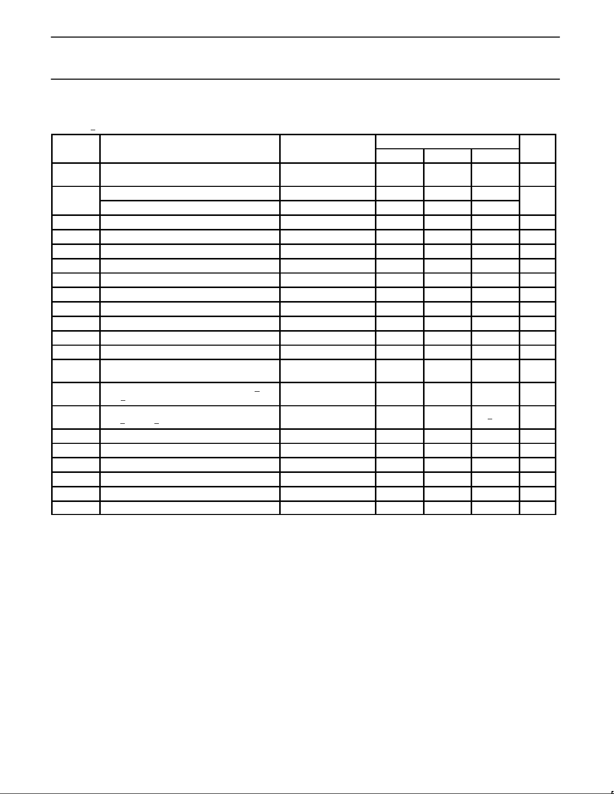
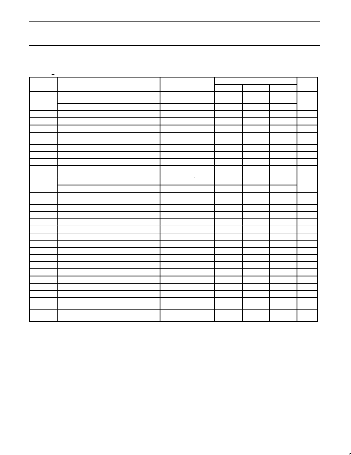
ELECTRICAL CHARACTERISTICS
VEE = –9V +5%; TA = 0°C to +70°C unless otherwise specified
1,2
. No external isolation
LIMITS
SYMBOL
PARAMETER
TEST CONDITIONS
MIN TYP MAX
UNIT
V
POR
Power–on reset voltage. Transmitter disabled
for |V
EE
| < |V
POR
|
–6.5 V
Supply current non–transmitting –80 –130
I
EE
Supply current transmitting –125 –180
mA
I
RXI
Receive input bias current V
RXI
= 0V –2 +25 µA
I
CDS
Cable sense input bias current V
CDS
= 0V +2 +6 µA
V
IH
HBE input HIGH voltage V
EE
+1.4 V
V
IL
HBE input LOW voltage V
EE
+0.4 V
I
IH
HBE input HIGH current V
HBE
= 0V 250 500 µA
I
IL
HBE input LOW current V
HBE
= V
EE
–500 –1000 µA
I
TDC
Transmit output DC current level
3
–37 –41 –45 mA
I
TAC
Transmit output AC current level
3
±28 ±I
TDC
mA
I
TX10
Transmit current V
TXO
= –10V –250 +250 µA
V
TCOM
Transmitter output voltage compliance
4
–3.7 V
V
CD
Collision threshold
5
Measured by applying
DC voltage at RXI
–1450 –1530 –1580 mV
V
OD
Differential output voltage – non idle at RX+ and
CD+
6
±600 ±1200 mV
V
OB
Differential output voltage imbalance – idle at
RX+
and CD+
7
+40 mV
V
OC
Output common mode voltage at RX± and CD± –1.5 –2 –2.5 V
V
RS
Receiver squelch threshold V
RXI
average DC –130 –250 –370 mV
V
TS
Transmitter squelch threshold (V
TX+
– V
TX–
) peak –175 –225 –300 mV
R
RXI
Shunt resistance at RXI non–transmitting 100 kΩ
C
RXI
Input capacitance at RXI 2 pF
R
TXO
Shunt resistance at TXO transmitting 10 kΩ
NOTES:
1. Currents flowing into device pins are positive. All voltages are referenced to ground unless otherwise specified. For ease of interpretation,
the parameter limit that appears in the MAX column is the largest value of the parameter, irrespective of sign. Similarly, the value in the MIN
column is the smallest value of the parameter, irrespective of sign.
2. All typicals are for V
EE
= –9V and TA = 27°C.
3. I
TDC
is measured as (V
MAX
+ V
MIN
)/(2 x 25) where V
MAX
and V
MIN
are the max and min voltages at TXO with a 25Ω load between TXO and
GND. I
TAC
is measured as (V
MAX
– V
MIN
)/(2 x 25).
4. The TXO pin shall continue to sink at least I
TDC
min when the idle (no signal) voltage on this pin is –3.7V .
5. Collision threshold for an AC signal is within 10% of V
CD
.
6. Measured on secondary side of isolation transformer (see Connection Diagram, Figure 1). The transformer has a 1:1 turns ratio with an
inductance between 30 and 100µH at 5MHz.
7. Measured as the voltage difference between the RX pins or the CD pins with the transformer removed.
Page 5
Philips Semiconductors Product specification
NE8392CCoaxial transceiver interface for Ethernet/Thin Ethernet
1995 May 1
5
TIMING CHARACTERISTICS
V
EE
= –9V +5%; TA = 0 to 70°C, unless otherwise specified1. No external isolation diode on TXO.
LIMITS
SYMBOL
PARAMETER
TEST CONDITIONS
MIN TYP MAX
UNIT
RON
Receiver start up delay RXI to RX± (Figure 3)
First received bit on RX±
V
RXI
= –2V peak 5
t
RON
First validly timed bit on RX± t
RON
+2
bits
t
RD
Receiver prop. delay RXI to RX± V
RXI
= –2V peak 35 50 ns
t
RR
Differential output rise time on RX± and CD±
2,3
5 ns
t
RF
Differential output fall time on RX± and CD±
2,3
5 ns
t
OS
Differential output settling time on RX± and CD±
to V
OB
= 40mV2 (see Figure 4)
1 µs
t
RJ
Receiver and cable total jitter ±3 ns
t
RHI
Receiver high to idle time Measured to +210mV 150 850 ns
t
RM
Rise and fall time matching on RX± and CD± tRF – t
RR
0.4 ns
Transmitter start–up delay TX± to TXO
(Figure 5)
TX
± = –1V peak
t
TST
First transmitted bit on TXO
VTX± = –1V peak
1 2
bits
First validly timed bit t
TST
+ 2
t
TD
Transmitter prop delay TX± to TXO
(see Figure 5)
VTX± = 1V peak 35 50 ns
t
TR
Transmitter rise time 10% to 90% (see Figure 5) 25 ns
t
TF
Transmitter fall time 10% to 90% (see Figure 5) 25 ns
t
TM
tTF – tTR mismatch ±2 ns
t
TS
Transmitter added skew
4
±2 ns
t
TON
Transmitter turn on pulse width (see Figure 5) VTX± = 1V peak 10 40 ns
t
TOFF
Transmitter turn off pulse width (see Figure 5) VTX± = 1V peak 150 250 340 ns
t
CON
Collision turn on delay (see Figure 6) 0V to –2V step at RXI 13 bits
t
COFF
Collision turn off delay (see Figure 6) –2V to 0V step at RXI 16 bits
t
CHI
Collision high to idle time (see Figure 6) Measured to +210mV 150 850 ns
f
CD
Collision frequency (see Figure 6) 8.0 10 12.5 MHz
t
CP
Collision signal pulse width (see Figure 6) 35 70 ns
t
HON
Heartbeat turn on delay (see Figure 7) 0.6 1.6 µs
t
HW
Heartbeat test duration (see Figure 7) 0.5 1.5 µs
t
JA
Jabber activation delay measured from TX± to
CD± (see Figure 8)
20 60 ms
t
JR
Jabber reset delay measured from TX± to CD±
(see Figure 8)
250 750 ms
NOTES:
1. All typicals are for V
EE
= –9V and TA = 27°C.
2. Measured on secondary side of isolation transformer (see Figure 1, Connection Diagram). The transformer has a 1:1 turn ratio with an
inductance between 30 and 100µH at 5MHz.
3. The rise and fall times are measured as the time required for the differential voltage to change from –225mV to +225mV , or +225mV to
–225mV, respectively.
4. Difference in propagation delay between rising and falling edges at TXO.
FUNCTIONAL DESCRIPTION
The NE8392C contains four main functional blocks (see Block
Diagram). These are:
a. The receiver which takes data from the coaxial cable and sends
it to the DTE.
b. The transmitter which receives data from the DTE and sends it
onto the coaxial cable.
c. The collision detection and heartbeat generation circuitry which
indicates to the DTE any collision on the coaxial cable and tests
for collision circuitry functionality at the end of every
transmission.
d. The jabber timer which disables the transmitter in the event of a
longer than legal length data packet.
Receiver Functions
The receiver consists of an input buffer, a cable equalizer, a 4-pole
Bessel low pass filter, a squelch circuit and a differential line driver.
The buffer provides high input resistance and low input capacitance
to minimize loading and reflections on the coaxial cable.
t
V
bits
Page 6

Philips Semiconductors Product specification
NE8392CCoaxial transceiver interface for Ethernet/Thin Ethernet
1995 May 1
6
The equalizer is a high pass filter that compensates for the low pass
effect of the coaxial cable and results in a flatband response over all
signal frequencies to minimize signal distortion.
The 4-pole Bessel low pass filter extracts the average DC voltage
level on the coaxial cable for use by the receiver squelch and
collision detection circuits.
The receiver squelch circuit prevents noise on the coaxial cable
from falsely triggering the receiver in the absence of a true signal.
At the beginning of a packet, the receiver turns on when the DC
level from the low pass filter is lower than the DC squelch threshold.
For normal signal levels this will take less than 500ns, or 5 bits.
However, at the end of a packet, a fast receiver turn off is needed to
reject both dribble bits on the coaxial cable and spurious responses
due to settling of the on-chip bandpass filter. This is accomplished
by an AC timing circuit that disables the receiver if the signal level
on the coaxial cable remains high for typically 250ns and only
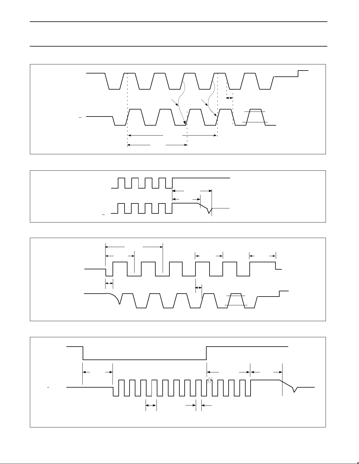
enables the receiver again after approximately 1µs. Figures 3 and 4
illustrate receiver timing.
The differential line driver provides typically ±
900mV signals to the
DTE with less than 7ns rise and fall times. When in idle state (no
received signal) its outputs provide <20mV differential voltage offset
to minimize DC standing current in the isolation transformer. The
line driver outputs are emitter followers and, for Ethernet
applications where they drive a 78Ω
transmission line, require a
500Ω pull-down resistor to VEE. For Thin Ethernet applications
where the AUI cable is not used, the pull-down resistor can be
increased to 1.5kΩ to save power consumption.
Transmitter Functions
The transmitter has differential inputs and an open collector current
driver output. The differential input common mode voltage is
established by the CTI and should not be altered by external
circuitry. Controlled rise and fall times of 25ns (+
5ns) minimize
higher harmonic components in the transmitted spectrum, while
matching of these rise and fall times to typically 2ns minimizes
signal jitter. The drive current levels of the CTI are set by an on-chip
bandgap voltage reference and an external 1% resistor. An on-chip
isolation diode is provided to reduce the transmitter’s coaxial cable
load capacitance. For Thin Ethernet applications, no further external
isolation diode is required, since the NE8392C meets the capacitive
loading specifications. For Ethernet applications a further external
diode should be added to reduce loading capacitance.
The transmitter squelch circuit ensures that the transmitter can only
be enabled by negative-going differential signals of typically greater
than 225mV in magnitude and 15ns in duration. The transmitter will
be disabled at the end of a packet if there are no negative going
signals of greater than 225mV for more than typically 250ns. Figure
5 illustrates transmitter timing.
Collision Functions
The collision detection scheme implemented in the NE8392C is
receive mode detection, which detects a collision between any two
stations on the network with certainty at all times, irrespective of
whether or not the local DTE is producing one of the colliding
signals. This is the only detection scheme allowed by the IEEE
802.3 standard for both repeater and non-repeater nodes.
The collision circuitry consists of the 4-pole Bessel low pass filter, a
comparator, a precision voltage reference that sets up the collision
threshold, a heartbeat generator, a 10MHz oscillator, and a
differential line driver .
The collision comparator monitors the DC level at the output of the
low pass filter and enables the line driver if it is more negative than
the collision threshold. A collision condition is indicated to the DTE
by a 10MHz oscillation signal at the CD outputs and typically occurs
within 700ns of the onset of the collision. The collision signal begins
with a negative-going pulse and ends with a continuous high-to-idle
state longer than 170ns. Figure 6 illustrates collision timing.
At the end of every transmission, the heartbeat generator creates a
pseudo collision to ensure that the collision circuitry is properly
functioning. This pseudo collision consists of a 1µs burst of 10MHz
oscillation at the line driver outputs approximately 1µs after the end
of the transmission. The heartbeat function can be disabled
externally by connecting the HBE (heartbeat enable) to V
EE
. This
allows the CTI to be used in repeater applications. Figure 7
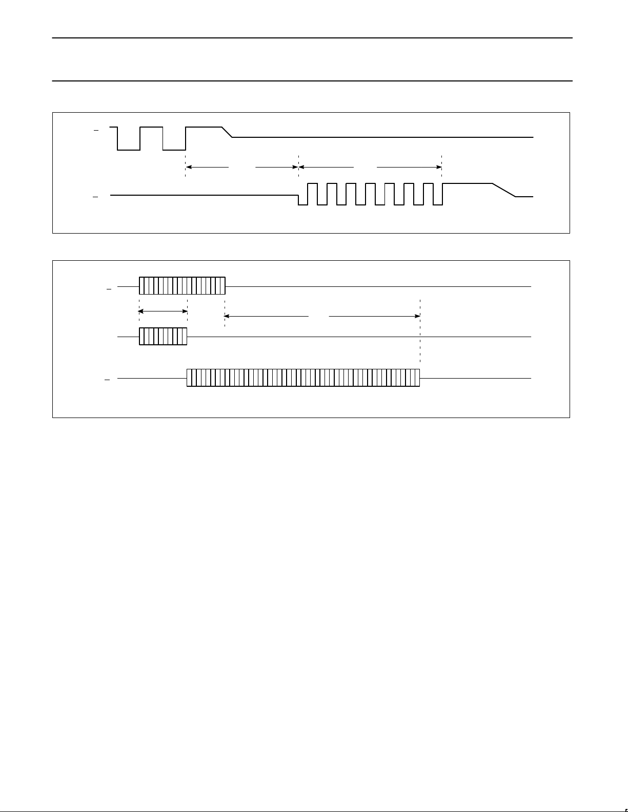
illustrates heartbeat timing.
As with the receiver outputs, the collision outputs also require a pull
down resistor to V
EE
and maintain <20mV differential voltage offset
in the idle state to minimize DC standing current in the isolation
transformers.
Jabber Functions
The jabber timer monitors the transmitter and inhibits transmission if
it is active for longer than typically 30ms. The jabber circuit then
enables the collision outputs for the remainder of the data packet
and for typically 450ns (unjab time) after it has ended. At this point
the transmitter becomes uninhibited. Figure 8 illustrates jabber
timing.
Detection of Coaxial Cable Faults
In the NE8392C there is no internal loopback path from the TX
inputs to the RX outputs. This means that, when the local DTE is
transmitting, the signal will only be present at the receiver outputs
RX+ and RX– if it appears on the coaxial cable and is larger than
the receiver squelch threshold V
RS
. If a short circuit fault condition
occurs at the cable connector to the CTI, then no signal will appear
at the receiver outputs. An intelligent DTE can, therefore, detect this
fault. If the fault is an open circuit, then a continuous collision signal
will be sent to the DTE, provided the average DC voltage at the RXI
pin is greater than the typical collision threshold of –1.53V .
If a short or open circuit occurs elsewhere on the coaxial cable, the
resulting reflections can result in an impedance at the CTI of any
value between a short circuit and 50Ω, depending on the distance of
the CTI from the fault. The upper limit of 50Ω results from the fact
that the coaxial cable is terminated in 50Ω at both ends. Faults on
the cable itself are, therefore, not guaranteed to be detected by
simply monitoring the RX and CD pins when in the transmit mode,
and more sophisticated schemes may be necessary.
Page 7
Philips Semiconductors Product specification
NE8392CCoaxial transceiver interface for Ethernet/Thin Ethernet
1995 May 1
7
CD+
CD–
RX+
V
EE1
V
EE2
RX–
TX+
TX–
HBE
GND
RR+
V
EE3
RXI
TXO
CDS
RR–
500Ω
500Ω
500Ω
500Ω
+
9V (ISOLATED)
–
DC TO DC
CONVERTER
78Ω
TRANSMIT
PAIR
RECEIVE
PAIR
COLLISION
PAIR
12 TO 15V DC
1K 1%
(NOTE 2)
NOTES:
1. T1 is a 1:1 pulse transformer, with an inductance of 30 to 100µH.
2. IN916 or equivalent for Ethernet, not required for Thin Ethernet.
3. 78Ω resistors not required if AUI cable not present.
4. Resistor value can be higher to reduce current consumption if AUI cable is not used.
78Ω
78Ω
NE8392C
CTI
1
2
3
4
5
6
7
8
16
15
14
13
12
11
10
9
1
2
4
5
7
8
16
15
13
12
10
9
T1 (NOTE 1)
COAX
DTE
AUI
CABLE
SD00289
(NOTE 4)
(NOTE 3)
SERIAL
NETWORK
INTERFACE
NETWORK
INTERFACE
CONTROLLER
I
S
O
L
A
T
I
O
N
DTE
COAX
B
U
S
NE8392C
COAX
TRANSCEIVER
INTERFACE
MAU
(OPTIONAL)
(AUI CABLE)
MAU = Medium Attachment Unit
AUI Cable = Attachment Unit Interface Cable (not used in Thin Ethernet applications)
SD00284
Figure 2. Interface Diagram for Ethernet/Thin Ethernet Local Area Network
Figure 1. Connection Diagram
Page 8
Philips Semiconductors Product specification
NE8392CCoaxial transceiver interface for Ethernet/Thin Ethernet
1995 May 1
8
10%
t
RD
t
RR
90%
t
RF
t
RON
+2
t
RON
PHASE VIOLATION
ALLOWED
VALID
TIMING
RXI
RX
+
1 2 3 4 5 6 7 8 9 10 11
1 2 3 4 5 6 7 8 9 10 11
SD00277
Figure 3. Receiver Timing
t
OS
RXI
RX
+
t
RHI
SD00279
10%
90%
t
TF
t
TR
t
TD
t
TON
t
TST
+2
t
TST
t
TOFF
TX+
TXO
100ns
1 2 3 4 5 6 7 8 9 10 11
1 2 3 4 5 6 7 8 9 10 11
SD00278
Figure 5. Transmitter Timing
t
CON
t
CP
RXI
CD+
t
COFF
t
CHI
1/F
CD
–2V
0V
SD00280
Figure 6. Collision Timing
Figure 4. Receiver End–of–Packet Timing
Page 9
Philips Semiconductors Product specification
NE8392CCoaxial transceiver interface for Ethernet/Thin Ethernet
1995 May 1
9
TX+
CD+
t
HON
t
HW
SD00281
TX+
CD+
t
JA
t
JR
TXO
SD00282
Figure 7. Heartbeat Timing
Figure 8. Jabber Timing
 Loading...