

Page 1

Philips Semiconductors Product specification
NE5900Call progress decoder
DESCRIPTION
The NE5900 call progress decoder (CPD) is a low cost, low power
CMOS integrated circuit designed to interface with a
microprocessor-controlled smart telephone capable of making
preprogrammed telephone calls. The call progress decoder
information to permit microprocessor decisions whether to initiate,
continue, or terminate calls. A tri-state, 3-bit output code indicates
the presence of dial tone, audible ring-back, busy signal, or re-order
tones.
A front-end bandpass filter is accomplished with switched
capacitors. The bandshaped signal is detected and the cadence is
measured prior to output decoding. In addition to the three data bits,
a buffered bandpass output and envelope output are available. All
logic inputs and outputs can interface with LSTTL, CMOS and
NMOS.
Circuit features include low power consumption and easy
application. Few and inexpensive external components are
required. A typical application requires a 3.58MHz crystal or clock,
470kΩ resistor, and two bypass capacitors. The NE5900 is ef fective
where traditional call progress tones, PBX tones, and precision call
progress tones must be correctly interpreted with a single circuit.
FEATURES
•Fully decoded tri-state call progress status output
•Works with traditional, precision, or PBX call progress tones
•Low power consumption
•Low cost 3.58MHz crystal or clock
•No calibration or adjustment
•Interfaces with LSTLL, CMOS, NMOS
•Easy application
PIN CONFIGURATION
D1 and N Packages
INPUT
1
V
2
REF
XTAL2
3
4
5
6
7
8
0V
TOP VIEW
EXT CLOCK IN/XTAL1
TEST IN
CLEAR IN
COUNT IN PROGRESS
NOTE:
1. SOL — Released in large SO package only.
Figure 1. Pin Configuration
APPLICATIONS
•Modems
•PBXs
•Security equipment
•Auto dialers
•Answering machines
•Remote diagnostics
•Pay telephones
5V
16
ANALOG OUT
15
TRI-STATE ENABLE
14
ENVELOPE
13
BIT 1
12
BIT 2
11
10
BIT 3
9
DATA VALID
SR01142
ORDERING INFORMATION
DESCRIPTION TEMPERATURE RANGE ORDER CODE DWG #
16-Pin Plastic Small Outline (SOL) Package
16-Pin Plastic Dual In-Line (DIP) Package
0 to +70°C
0 to +70°C
NE5900DK SOT162-1
NE5900N SOT38-4
1986 May 8 853-0842 83667
1
Page 2

Philips Semiconductors Product specification
NE5900Call progress decoder
BLOCK DIAGRAM
ANALOG OUT 0V 5V
V
REF
INPUT
EXT CLOCK
IN/XTAL1
XTAL2
FILTER
TIMING
10kΩ
DETECTOR
DECODER
TESTINCLEARINCOUNT IN
PROGRESS
10kΩ
DATA
VALID
TRI-STATE
TRI-STATE
ENABLE
ENVELOPE
BIT 1
BIT 2
BIT 3
Figure 2. NE5900 Block Diagram
ABSOLUTE MAXIMUM RATINGS
SYMBOL PARAMETER RATING UNITS
V
DD
V
IN
V
IN
V
OUT
T
STG
T
A
T
SOLD
T
JMAX
NOTE:
1. Includes Pin 3 — Ext Clock In
Supply voltage 9 V
Logic control input voltages -0.3 to +16 V
All other input voltages
1
-0.3 to VCC + 0.3 V
Output voltages -0.3 to VCC + 0.3 V
Storage temperature range -65 to +150 °C
Operating temperature range 0 to +70 °C
Lead soldering temperature (10s) +300 °C
Junction temperature +150 °C
SR01143
1986 May 8
2
Page 3

Philips Semiconductors Product specification
SYMBOL
PARAMETER
TEST CONDITIONS
UNITS
NE5900Call progress decoder
DC ELECTRICAL CHARACTERISTICS
VCC = +3.3V , TA = 25°C; unless otherwise stated.
LIMITS
MIN TYP MAX
Pin 16
DD
DD
= V
= V
REF
REF
Pin 14 = V
Pin 5, 6 = 0V
DD
Output Pin 13 = V
Output Pin 13 = 0V
Pin 1 frequency, 0dB max.,
= V
DC
Output Pin 13 = 0V
REF
Pin 1 frequency, 0dB max.,
= V
DC
Output Pin 13 = 0V
REF
DD
I
= 1.6mA
SINK
Pins 7, 9, 10, 11, 12, 13
I
Pins 7, 9, 10, 11, 12, 13
V
Pins 10, 11, 12, 13,
SOURCE
= VDD or 0V
OUT
= 0.5mA
Pin 14 = 0V
Input Pin 1, 460Hz – 20dB,
= V
V
DC
Output Pin 15,
REF
= 1MΩ
R
LOAD
enced to 460Hz
= V
DC
to response of Pin 13
REF
DD
on Pin 1)
4.5 5.0 5.5 V
-39 -35 dB
-50 dB
180 Hz
800 Hz
-1.0 1.0 µA
DD
0 0.4 V
VDD – 0.4 V
DD
-3.0 3.0 µA
6.5 8.5 10.5 dB
-1.0 1.0 dBmo
38 ms
1
1
V
V
V
Power supply voltage
DD
Quiescent current As above with no output loads 2.0 4.0 mA
Input threshold
Signal rejection
Low frequency2 rejection
High frequency2 rejection
V
V
V
V
V
V
I
Logic 1 level Pins 6, 14 2.0 15 V
IH
Logic 0 level Pins 6, 14 0 0.8 V
IL
I
Logic 1 input current Pins 3, 6, 14 = V
IH
I
Logic 0 input current Pins 3, 6, 14 = 0V -1.0 1.0 µA
IL
Logic 1 input voltage Pin 3 External Clock In/XTAL VDD – 1 V
IH
Logic 0 input voltage Pin 3 External Clock In/XTAL 0 1.0 V
IL
Logic 0 output voltage
OL
Logic 1 output voltage
OH
Tri-state leakage
OZ
Filter output gain
Filter frequency response
Input impedance Pin 1, frequency = 460MHz 1 MΩ
V
R
Reference voltage Pin 2, VDD = 5V 2.4 2.5 2.6 V
REF
Reference resistance Pin 2 5 Ω
REF
Envelope response time
NOTE:
1. 0dB = 0.775V
2. By design; not tested.
RMS
Pin 1 level, frequency = 460Hz,
V
Pin 1 level, frequency = 300Hz,
V
V
V
As above from 300Hz to 630Hz, refer-
Time from removal or application of
460Hz – 20dB (V
The NE5900 uses the signal in the call progress tone passband and
the cadence of interrupt rate of the signal to determine which call
progress tone is present.
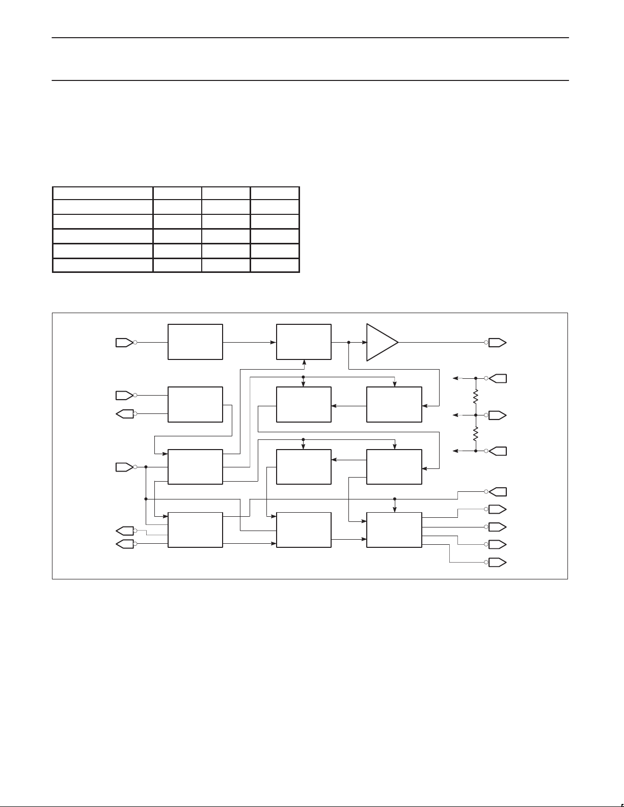
Figure 3 shows a detailed block diagram of the NE5900.
The signal input from the phone line is coupled through a 470kΩ
resistor which, together with two internal capacitors and an internal
resistor, form an anti-aliasing filter. This passive low pass filter
strongly rejects AM radio interference. Insertion loss is typically
1.5dB at 460Hz. The 470kΩ resistor also provides protection from
the transients. The input (Pin 1) DC voltage can be derived from
V
(Pin 2) or allowed to self-bias through a series coupling
REF
capacitor (10nF minimum).
Following this is a switched capacitor bandpass filter which accepts
call progress tones and inhibits tones not in the call progress band
of 300Hz to 630Hz. The bandpass limits are determined by the
1986 May 8
input clock frequency of 3.58MHz. An on-board inverter between
Pins 3 and 4 can be used either as a crystal oscillator or as a buffer
for an external 3.58MHz clock signal. The switched capacitor filters
provide typical rejection of greater than 40dB for frequencies below
120Hz and above 1.6kHz.
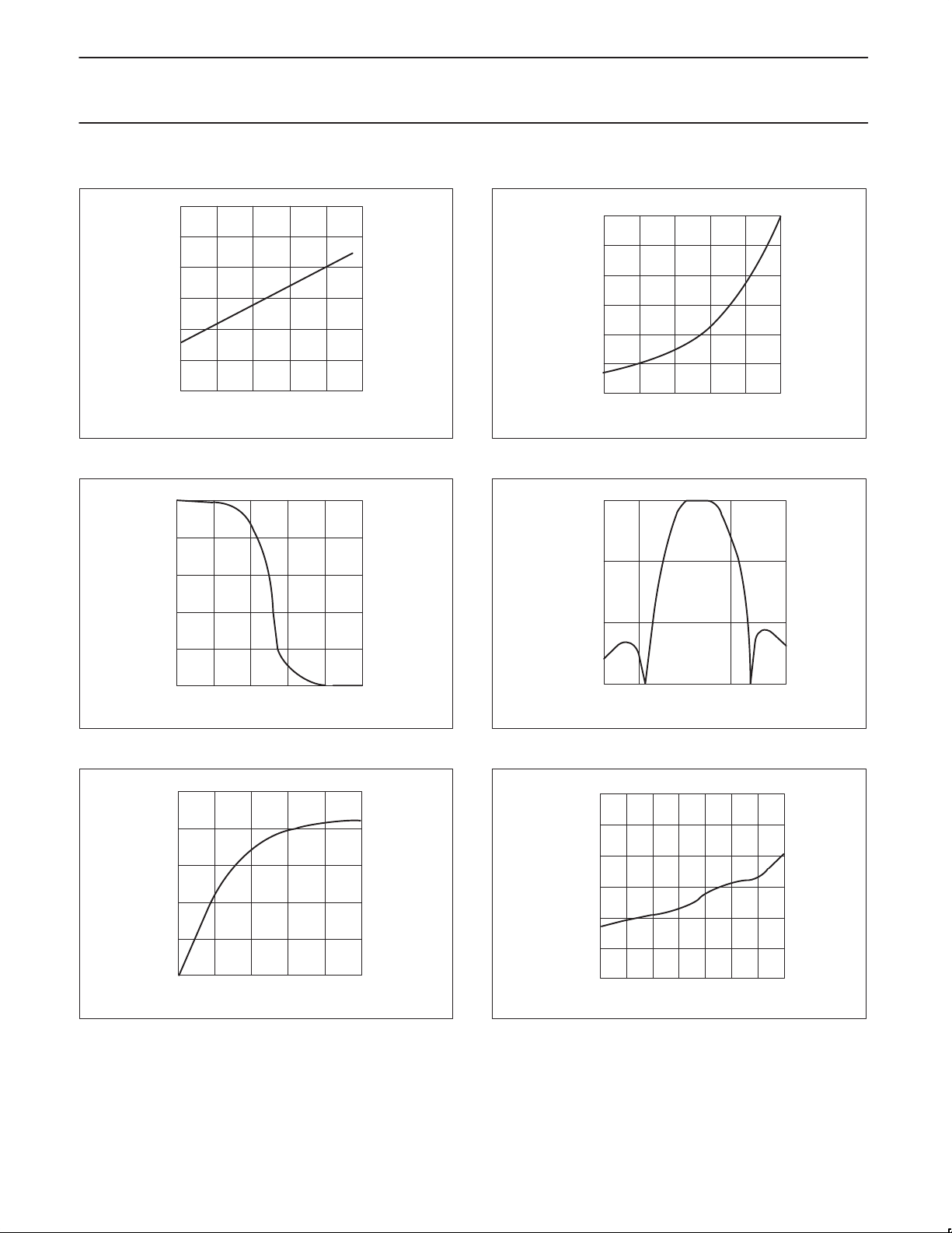
The decoder responds to signals between 300Hz and 630Hz with a
threshold of -39dB typical (0dB = 0.775V
respond to any signal below -50dB or to tones up to 0dB which are
). The decoder will not
RMS
below 180Hz or above 800Hz. Dropouts of 20ms or bursts of only
20ms duration are ignored. A gap of 40ms or a valid tone of 40ms is
detected.
The buffered output of the switched capacitor filter is available at the
analog output, Pin 15. A logic output representing the detected
envelope of this signal is available at the envelope output, Pin 13.
3
Page 4
Philips Semiconductors Product specification
NE5900Call progress decoder
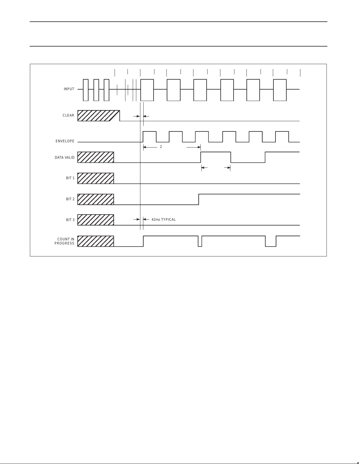
At the start of an in-band tone (envelope output goes high), a 2.3
second interval is timed out. Transitions of the envelope during this
interval are counted to determine the signal present. At 2.3
seconds, the three bits of data representing this decision are stored
in the latch and appear at the outputs. A data valid signal goes high
at this time, signaling that the data bits, Pins 10 – 12, can be read.
The output code is as follows:
Pin 12 Pin 11 Pin 10
Dial Tone 0 0 0
Ringing Signal 1 0 0
Busy Signal 0 1 0
Re-order Tone 0 0 1
Overflow 1 1 1
The overflow condition occurs in the event that too many transitions
occur during the 2.3 second interval. This can result from noise,
voice, or other line disturbances not normally present during the
INPUT
EXT CLOCK
IN/XTAL1
IN/XTAL2
ANTI-ALIAS
FILTER
3.58MHz
OSCILLATOR
SC BANDPASS
FILTER
LOWPASS
FILTER
post-dialing interval. Note that the end of dial tone in interpreted as
a valid ringing signal.
The clear input resets all internal registers and the output latch, and
is to be set low after the completion of dialing. The clear input
should be pulsed high for proper operation. Recommended pulse
width is between 0.2µs and 20ms. If clear is held high when
envelope is high, a false output pulse (Pin 13) can result when clear
is returned low.
For applications where dialing is done by a person rather than by a
microprocessor, an uncertainty exists about the number of digits to
be dialed (local vs long distance). In such situations it is possible to
clear the NE5900 by application of the DTMF signal or dial pulses to
the clear pin (Pin 6). When dialing is complete, the device is cleared
and ready to respond to the next call progress unit.
Enable is held at 5V to enable Pins 10, 11, 12 and 13. When enable
is brought low, data valid is also set low. Enable must remain high
while the data is also set low. Enable must remain high while the
data is being read. The test pin is for production test only and must
be kept low in all user applications.
BUFFER
5V
R1
DIGITAL
DETECTOR
10kΩ
R2 10kΩ
V
REF
CLEAR
COUNT IN
PROGRESS
DATA VALID
IN
CLOCK
DIVIDERS
2.3 SECOND
TIMER
Figure 3. Detailed Block Diagram CPD
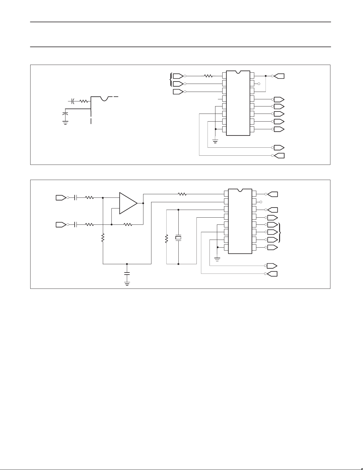
Figure 4 shows a typical application of the call progress decoder.
In this application only one external component is needed an no
microprocessor activity other than clear is required.
Figure 5 shows the recommended direct interface to the telephone
line. Bus connection is possible by utilizing tri-state, and internal
timing is accomplished with a 3.58MHz crystal.
DECODER
LOGIC
DECODER
LATCHES
0V
ANALOG
DETECTOR
TRI-STATE
ENABLE
ENVELOPE
TRI-STATE
BUFFERS
BIT 1
BIT 2
BIT 3
SR01144
The designer can utilize the input signal, clock, bus, or
microprocessor interface which best serves the application. Figure
6 gives a typical timing diagram for the application of Figures 4 and
5.
1986 May 8
4
Page 5
Philips Semiconductors Product specification
NE5900Call progress decoder
10nF1470kΩ
10nF
IN1
IN2
CAPACITIVE
C1
10nF
C2
10nF
2
OPTIONAL
INPUT
R1
100kΩ
R2
100kΩ
R3
100kΩ
+
A
–
100kΩ
V
R4
TO EAR-PIECE
3.58MHz IN
Figure 4. Typical Application
R5
470kΩ
R6
10MΩ
3.58MHz
470kΩ
1
2
3
4
NE5900
5
6
7
8
1
2
3
4
5
6
7
8
NE5900
16
15
14
13
12
11
10
9
16
15
14
13
12
11
10
9
5V
ENVELOPE
BIT 1
BIT 2
BIT 3
INTERRUPT
START
CLEAR
5V
ENABLE
ENVELOPE
DECODED
OUTPUTS TO
PROCESSOR
INTERRUPT
SR01145
C3
1µF
Figure 5. Typical Two-Wire Application
START
CLEAR
SR01146
1986 May 8
5
Page 6
Philips Semiconductors Product specification
NE5900Call progress decoder
INPUT
CLEAR
ENVELOPE
DATA VALID
BIT 1
BIT 2
BIT 3
COUNT IN
PROGRESS
38ms TYPICAL
2.27 SECONDS
1.1 SECONDS
42ms TYPICAL
SR01147
Figure 6.
1986 May 8
6
Page 7
Philips Semiconductors Product specification
NE5900Call progress decoder
TYPICAL PERFORMANCE CHARACTERISTICS
3.0
2.5
2.0
1.5
1.0
0.5
SUPPLY CURRENT (mA) (Pin 16)
0.0
3.0 3.5 4.0 4.5 5.0 5.5
SUPPLY VOLTAGE (VDD) (Pin 16)
Figure 7. Power Supply Current vs V
5
4
3
2
OUTPUT VOLTAGE (Pin 4)
1
DD
SR01148
3.0
-2.5
-5.0
-7.5
-10.0
-12.5
OUTPUT CURRENT (mA) (Pin 13)
-15.0
012345
OUTPUT VOLTAGE (Pin 13)
SR01151
Figure 10. Output Voltage Current Curve Digital Output High
0
-20
-40
0
0
2
1
INPUT VOLTAGE (Pin 3)
345
Figure 8. Voltage Transfer Curve
50
40
30
20
10
OUTPUT CURRENT SINK (mA) (Pin 13)
0
0
234
1
OUTPUT VOLTAGE (Pin 13)
Figure 9. Digital Output Low
5
SR01149
SR01150
LEVEL RELATIVE TO 460Hz (dBV) (Pin 15)
-60
100 1000
FREQUENCY (40 TO 4000Hz)
Figure 11. Filter Frequency Response
-20
-25
-30
-35
Pin 1 LEVEL (dB)
-40
-45
-50
350 400 450 500 550 600 650
300
FREQUENCY (Hz)
Figure 12. Typical Threshold
SR01152
SR01153
1986 May 8
7
 Loading...