

Page 1

Philips Semiconductors Linear Products Product specification
NE587LED decoder/driver
530
August 31, 1994 853-1095 13721
DESCRIPTION
The NE587 is a latch/decoder/driver for 7-segment common anode
LED displays. The NE587 has a programmable current output up to
50mA which is essentially independent of output voltage, power
supply voltage, and temperature. The data (BCD) inputs and LE
(latch enable) input are low-loading so that they are compatible with
any data bus system. The 7-segment decoding is implemented with
a ROM so that alternative fonts can be made available.
FEATURES
•Latched BCD inputs
•Low loading bus-compatible inputs
•Ripple-blanking on leading- and/or trailing-edge zeros
APPLICATIONS
•Digital panel motors
•Measuring instruments
•Test equipment
•Digital clocks
•Digital bus monitoring
PIN CONFIGURATIONS
1
2
3
4
5
6
7
8
9
10
11
12
18
17
16
15
14
13
1
2
3
4
5
6
7
8
9
10
11
12
13
14
20
19
18
17
16
15
D
1
D
2
LE
BI/RBO
DIG GND
RBI
I
P
D
3
D
0
V
CC
f
g
a
POWER GND
b
e
c
d
D
1
D
2
LE
BI/RBO
DIG GND
RBI
I
P
D
3
D
0
V
CC
f
g
a
POWER GND
b
e
NC
d
NC
c
N Package
D1 Package
NOTE:
1. SOL and non-standard pinout.
ORDERING INFORMATION
DESCRIPTION TEMPERATURE RANGE ORDER CODE DWG #
20-Pin Plastic Small Outline Large (SOL) Package 0 to +70°C NE587D
1
0172D
18-Pin Plastic Dual In-Line Package (DIP) 0 to +70°C NE587N 0407A
NOTES:
1. SOL and non-standard pinout
ABSOLUTE MAXIMUM RATINGS
TA=25°C unless otherwise specified.
SYMBOL
PARAMETER RATING UNIT
V
CC
Supply voltage -0.5 to +7 V
V
IN
Input voltage
(D
0-D3
, LE, RBI)
-0.5 to +15 V
V
OUT
Output voltage
(a-g, RBO)
-0.5 to +7 V
P
D
Power dissipation (25°C)
1
1000 mW
T
A
Ambient temperature range 0 to 70 °C
T
J
Junction temperature 150 °C
T
STG
Storage temperature range -65 to +150 °C
T
SOLD
Soldering temperature (10sec max) 300 °C
NOTES:
1. Derate power dissipation as indicated
N package—95°C/W above 55°C
Page 2
Philips Semiconductors Linear Products Product specification
NE587LED decoder/driver
August 31, 1994
531
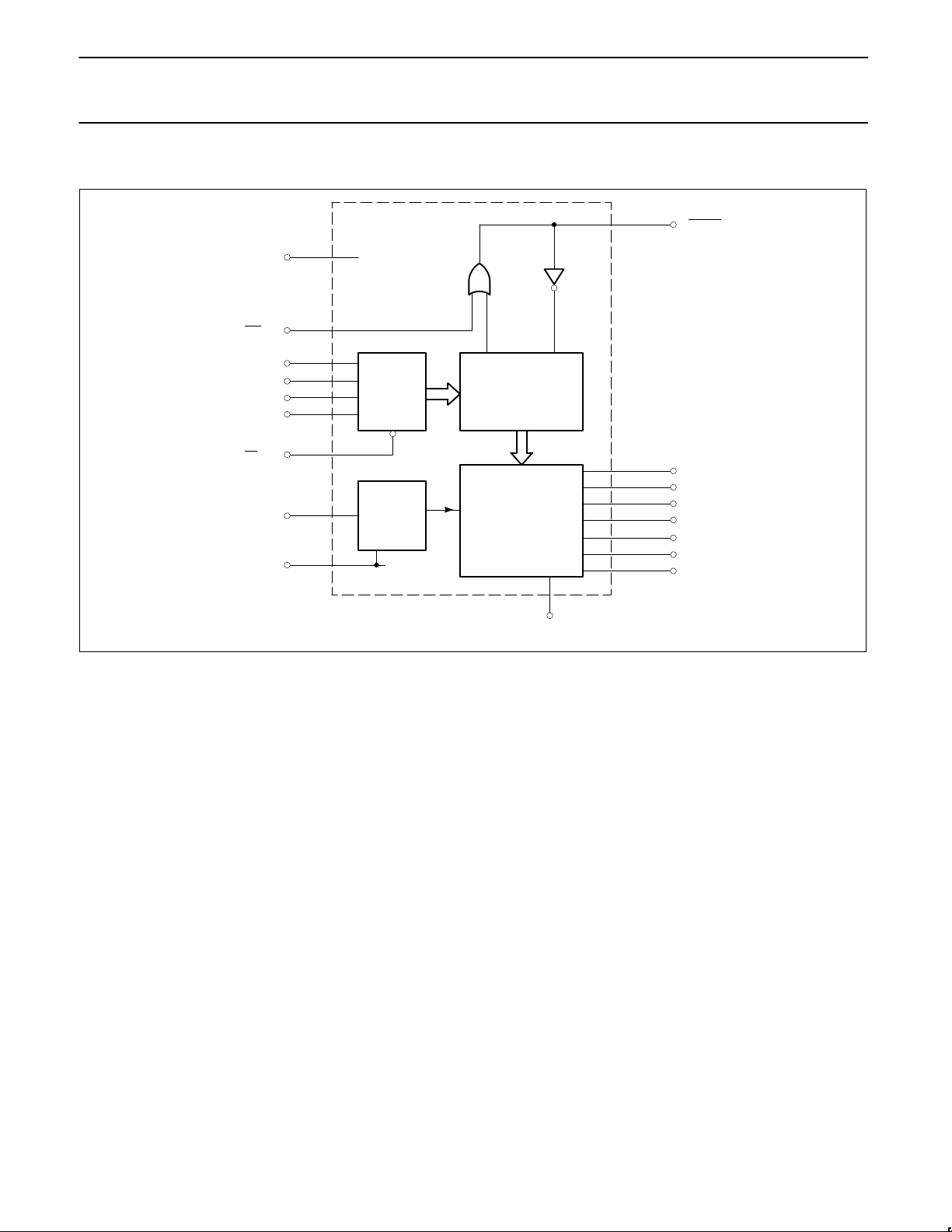
BLOCK DIAGRAM
..
..
D
1
D
2
LE
BI/RBO
GND
RBI
I
P
D
3
D
0
V
CC
f
g
a
POWER GND (10)
b
e
d
c
(18)
(5)
(7)
(1)
(2)
(6)
(3)
(8)
(9)
(4)
(15)
(14)
(13)
(12)
(11)
(17)
(16)
DATA
LATCHES
BCD TO
7-SEGMENT
DECODER
SEGMENT
CURRENT
DRIVER
BANDGAP
REFERENCE
Page 3
Philips Semiconductors Linear Products Product specification
NE587LED decoder/driver
August 31, 1994
532
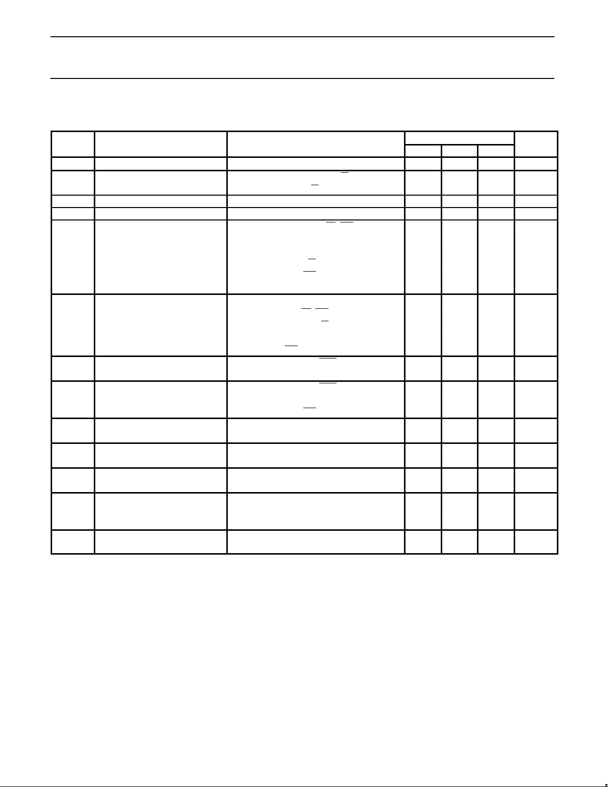
DC ELECTRICAL CHARACTERISTICS
VCC=4.75 to 5.25V, 0°C < T
A
< 70°C. Typical values are at VCC=5V, TA=25°C, RP=1kΩ (±1%), unless otherwise specified.
LIMITS
SYMBOL
PARAMETER
TEST CONDITIONS
Min Typ Max
UNIT
V
CC
Operating supply voltage 4.75 5.00 5.25 V
V
IH
Input high voltage All inputs except BI 2.0 15 V
BI 2.0 5.5
V
IL
Input low voltage 0.8 V
V
IC
Input clamp voltage IIN=-12mA, TA=25°C -1.5 V
Inputs D0-D3, LE, RBI µA
VIN=2.4V 1.0 10
I
IH
Input high current VIN=15V 15 15
Input BI (Pin 4) 10 100 µA
RBI=H
VIN=VCC=5.25V
VIN=0.4V, Inputs D0-D
3
-5
I
IL
Input low current LE, RBI -200 µA
Input BI
VCC=5.25V -0.7 mA
RBI=H, VIN=0.4V
V
OL
Output low voltage Output RBO 0.2 0.5 V
I
OUT
=3.0mA
Output RBO
V
OH
Output high voltage I
OUT
=-50µA 3.5 4.5 V
RBI=H
I
OUT
Output segment Outputs “a” through “g” 20 25 30 mA
“ON” current V
OUT
=2.0V
∆I
OUT
Output current ratio With reference to “b” segment 0.90 1.00 1.10
(all outputs ON) V
OUT
=2.0V
Output segment Outputs “a” through “g”
I
OFF
“OFF” current V
OUT
=5.0V 20 250 µA
VCC=5.25V
I
CCO
Supply current All outputs “ON” 33 55 mA
V
OUT
>1V
VCC=5.25V
I
CCI
Supply current All outputs blanked 50 70 mA
NOTES:
NE587 Programming:
The NE587 output current can be programmed, provided a program resistor, R
P
, be connected between IP (Pin 8) and Ground (Pin 9). The
voltage at I
P
(Pin 8) is constant (≈1.3V). Thus, a current through RP is IP ≈ 1.3V/RP, as shown in Figure 5. IO/IP is 20 in the 15 to 50mA output
current range.
Page 4
Philips Semiconductors Linear Products Product specification
NE587LED decoder/driver
August 31, 1994
533
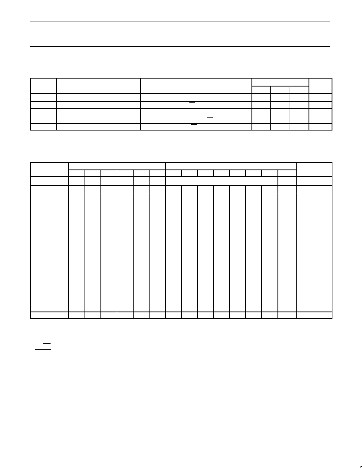
AC ELECTRICAL CHARACTERISTICS
VCC=5V, TA=25°C, RL=130Ω, CL=30pF including probe capacity.
LIMITS
SYMBOL
PARAMETER
TEST CONDITIONS
Min Typ Max
UNIT
t
DAV
Propagation delay (Figure 2) From data to output 135 ns
t
DAV
Propagation delay (Figure 3) From LE to output 135 ns
t
W
Latch enable pulse width (Figure 4) 30 ns
t
S
Latch enable setup time (Figure 4) From data to LE 20 ns
t
H
Latch enable hold time (Figure 4) From LE to data 0 ns
NOTES:
t
DAV
= (tHL+tLH)
TRUTH TABLE
BINARY
INPUTS OUTPUTS
BINARY
INPUT
LE RBI D
3
D
2
D
1
D
0
a b c d e f g RBO
DISPLAY
- H * X X X X
STABLE ** STABLE
0 L L L L L L H H H H H H H L
BLANK
0 L H L L L L L L L L L L H H 0
1 L X L L L H H L L H H H H H 1
2 L X L L H L L L H L L H L H 2
3 L X L L H H L L L L H H L H 3
4 L X L H L L H L L H H L L H 4
5 L X L H L H L H L L H L L H 5
6 L X L H H L L H L L L L L H 6
7 L X L H H H L L L H H H H H 7
8 L X H L L L L L L L L L L H 8
9 L X H L L H L L L L H L L H 9
10 L X H L H L H H H H H H L H 11 L X H L H H L H H L L L L H E
12 L X H H L L H L L H L L L H H
13 L X H H L H H H H L L L H H L
14 L X H H H L L L H H L L L H P
15 L X H H H H H H H H H H H H Blank
**BI X X X X X X H H H H H H H L** Blank
NOTES:
H=HIGH voltage level, output is “OFF”
L=LOW voltage level, output is “ON”
X=Don’t care
* The RBI
will blank the display only if a binary zero is stored in the latches.
** RBO/BI
used as an input overrides all other input conditions.
NE587 PROGRAMMING
587 output current can be programmed by using a programming
resistor, RP, connected between RP (Pin 8) and GND (Pin 9). The
voltage at RP (Pin 8) is constant (
K = 1.3V). A partial schematic of
the voltage reference used in the NE587 is shown in Figure 1.
Output current to program current ratio, I
O/IP
, is 20 in the 15mA to
50mA range. Note that I
P
must be derived from a resistor (RP), and
not from a high-impedance source such as an I
OUT
DAC used to
control display brightness.
POWER DISSIPATION CONSIDERATIONS
LED displays are power-hungry devices, and inevitably, somewhat
inefficient in their use of the power supply necessary to drive them.
Duty cycle control does afford one way of improving display
efficiency, provided that the LEDs are not driven too far into
saturation; but the improvement is marginal. Operation at higher
peak currents has the added advantage of giving much better
matching of light output, both from segment-to-segment and
digit-to-digit.
Page 5
Philips Semiconductors Linear Products Product specification
NE587LED decoder/driver
August 31, 1994
534
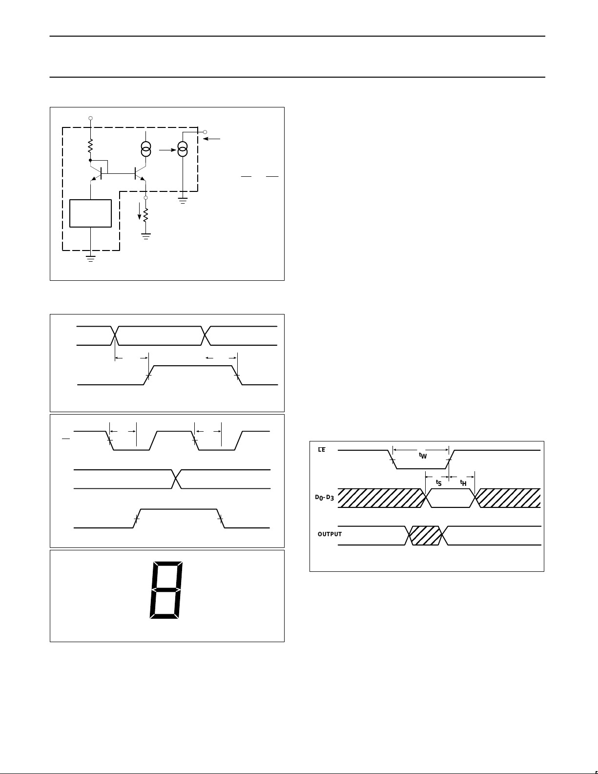
Figure 1.
I
P
V
rP
R
P
1.3V
R
P
R
P
I
P
I
O
V
CC
1:20
PIN 8
BAND GAP
REFERENCE
TIMING DIAGRAMS
Figure 2. tP Data to Output
LE = L
D0–D
3
OUTPUT
t
PLH
t
PHL
Figure 3. tP Latch Enable to Output
t
PLH
t
PHL
LE
D0–D
3
OUTPUT
Segment Identification
a
b
c
d
e
f
g
An output current of 10 to 50mA was chosen so that it would be
suitable for multiplexed operation of large-size LED digits. When
designing a display system, particular care must be taken to
minimize power dissipation within the IC display driver. Since the
output is a constant-current source, all the remaining supply voltage,
which is not dropped across the LED (and the digit driver, if used),
will appear across the output. Thus, the power dissipation will go up
sharply if the display power supply voltage rises. Clearly, then, it is
good design practice to keep the display supply voltage as low as
possible, consistent with proper operation of the supply output
current sources. Inserting a resistor or diode in series with the
display supply is a good way of reducing the power dissipation
within the integrated circuit segment driver, although, of course, total
system power remains the same.
Power dissipation may be calculated as follows. Referring to Figure
6, the two system power supplies are V
CC
and VS. In many cases,
these will be the same voltage. Necessary parameters are:
V
CC
Supply voltage to driver
V
S
Supply voltage to display
I
CC
Quiescent supply current of driver
I
SEG
LED segment current
V
F
LED segment forward voltage at I
SEG
K
DC
% Duty cycle
V
F
, the forward LED drop, depends upon the type of LED material
(hence the color) and the forward current. The actual forward
voltage drops should be obtained from the LED display
manufacturer’s literature for the peak segment current selected;
however, approximate voltages at nominal rated currents are:
Red 1.6 to 2.0V
Orange 2.0 to 2.5V
Yellow 2.2 to 3.5V
Green 2.5 to 3.5V
Figure 4. Setup and Hold Times
LE
D0–D
3
OUTPUT
t
W
t
S
t
H
Page 6
Philips Semiconductors Linear Products Product specification
NE587LED decoder/driver
August 31, 1994
535
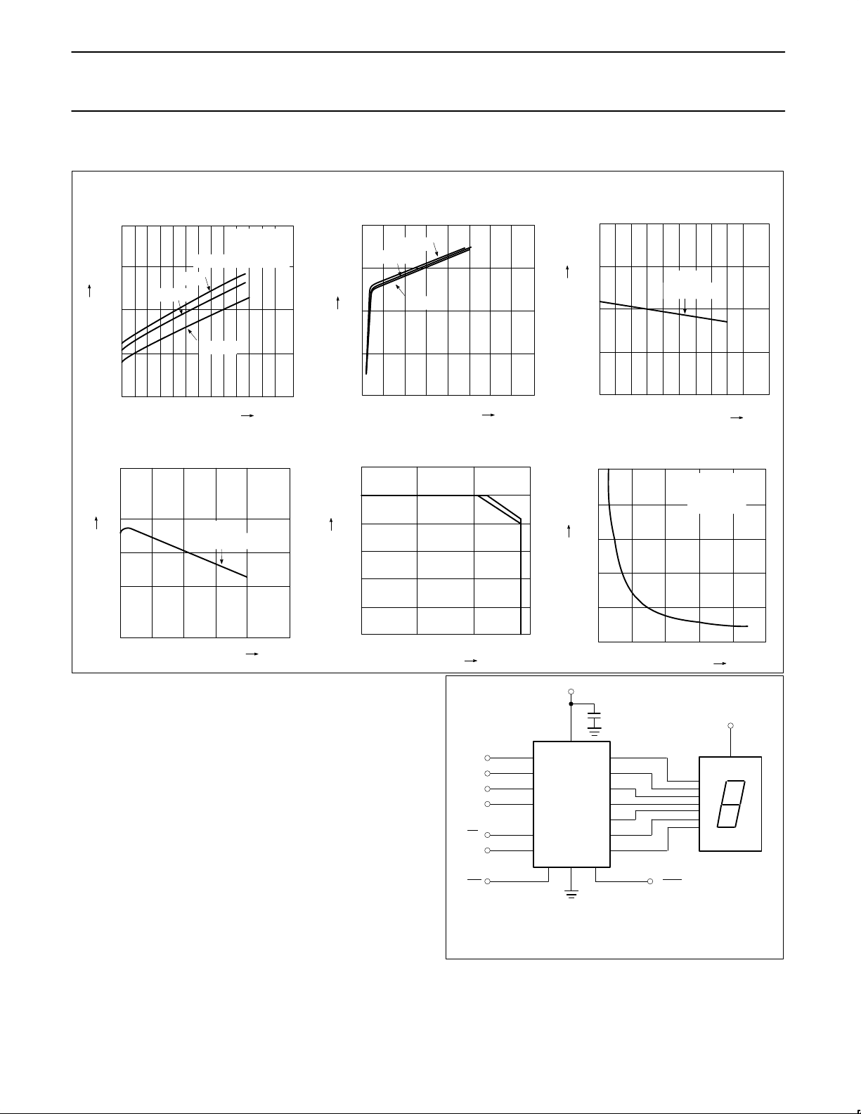
TYPICAL PERFORMANCE CURVES
I
OUT
(mA)
Supply Current vs Supply Voltage
Output Current vs Output Voltage
R
P
= 1kΩ
Normalized Output Current vs
Temperature VCC = 5.0V
Normalized Output Current vs Supply
Voltage V
O
= 2V, TA = 25°C
Maximum Power Dissipation vs
Temperature
Output Current vs Program Resistor
40.0
35.0
30.0
25.0
20.0
4.0 4.4 4.8 5.2 5.6 6.0 6.4
V
CC
(VOLTS)
I
CC
(mA)
RP = 1kΩ
V
OUT
= 2V
ALL OUTPUTS “ON”
(0°C)
(25°C)
(70°C)
40.0
30.0
20.0
10.0
I
OUT
0 1.0 2.0 3.0 4.0 5.0
V
OUT
(VOLTS)
(70°C)
(0°C)
(25°C)
RP = 1kΩ
(%)
I
OUT
TEMP (°C)
110.0
105.0
100.0
95.0
90.0
10 20 30 40 50 60 70 80
105
102
100
98
95
4.0 4.5 5.0 5.5 6.0
(%)
NE587
RP = 1kΩ
NE587
VCC (VOLTS)
1000
800
600
400
200
0
0 25 50 75
T
A
(°C)
(mW)
P
D
50.0
40.0
30.0
20.0
10.0
0.0
0 2.0 4.0 6.0 8.0 10.0
VCC = 5.0V
V
OUT
= 2V
TA = (25°C)
RP (kΩ)
(mA)
I
OUT
These voltages are all for single-diode displays. Some early red
displays had 2 series LEDs per segment; hence the forward voltage
drop was around 3.5V.
Thus, a maximum power dissipation calculation when all segments
are on, is:
P
D
+ VCCx ICC) (VS* VF) x 7 x I
SEG
x KDCmW
Assuming V
S
= V
CC
= 5.25V
V
F
= 2.0V
K
DC
= 100%
P
D MAX
= 5.25 × 50 + 3.25 × 7 × 30mW = 945mW
However, the average power dissipation will be considerably less
than this. Assuming 5 segments are on (the average for all output
code combinations), then
P
D MAX
= 5.0 × 30 + 3.00 × 5 × 25mW = 525mW
Operating temperature range limitations can be deduced from the
power dissipation graph. (See Typical Performance Characteristics.)
Figure 5. Driving a Single Digit
V
S
V
CC
D
3
D
2
D
1
D
0
I
P
Decoupling capacitor on VCC should be 0.01µF ceramic.
LE
RBI RBO
0.01µF
NOTE:
NE587
a
b
c
d
e
f
g
Page 7
Philips Semiconductors Linear Products Product specification
NE587LED decoder/driver
August 31, 1994
536
However, a major portion of this power dissipation (P
D MAX
) is
because the current source output is operating with 3.25V across it.
In practice, the outputs operate satisfactorily down to 0.5V , and so
the extra voltage may be dropped external to the integrated circuit.
Suppose the worst-case V
CC/VS
supply is 4.75 to 5.25V, and that
the maximum V
E
for the LED display is 2.25V. Only 2.75V is
required to keep the display active, and hence 2.0V may be dropped
externally with a resistor from V
CC
to VS. The value of this resistor is
calculated by:
R
S
+
2.0
7 x I
SEG
[ 10 (
1
2
W rating)
assuming worst case I
SEG
of 30mA.
Hence now
P
D MAX
= V
CC
× I
CC
+
(V
S
- V
V
- R
X
× 7 × I
SEG
) × 7 × I
SEG
× K
DC
= 5.25 × 50 + 1.25 × 7 × 30mW
= 525mW
and
P
D av
= 5.0 × 30 + 1.25 × 5 × 25 = 306 mW.
If a diode (or 2) is used to reduce voltage to the display, then the
voltage appearing across the display driver will be independent of
the number of “ON” segments and will be equal to
V
S
- V
F
- nVd, VD≈ 0.8V
Where n is the number of diodes used, power dissipation can be
calculated in a similar manner.
In a multiplexed display system, the voltage drop across the digit
driver must also be considered in computing device power
dissipation. It may even be an advantage to use a digit driver which
drops an appreciable voltage, rather than the saturating PNP
transistors shown in Figure 9. For example a Darlington PNP or
NPN emitter-follower may be preferable. Figure 8 shows the NE591
as the digit driver in a multiplexed display system. The NE591 output
drops about 1.8V which means that the power dissipation is evenly
distributed between the two integrated circuits.
Where V
S
and VCC are two different supplies, the VS supply may be
optimized for minimum system power dissipation and/or cost.
Clearly, good regulation in the V
S
supply is totally unnecessary, and
so this supply can be made much cheaper than the regulated 5V
supply used in the rest of the system. In fact, a simple unsmoothed
full-wave rectified sine wave works extremely well if a slight loss in
brightness can be tolerated. A transformer voltage of about
3-4.5V
RMS
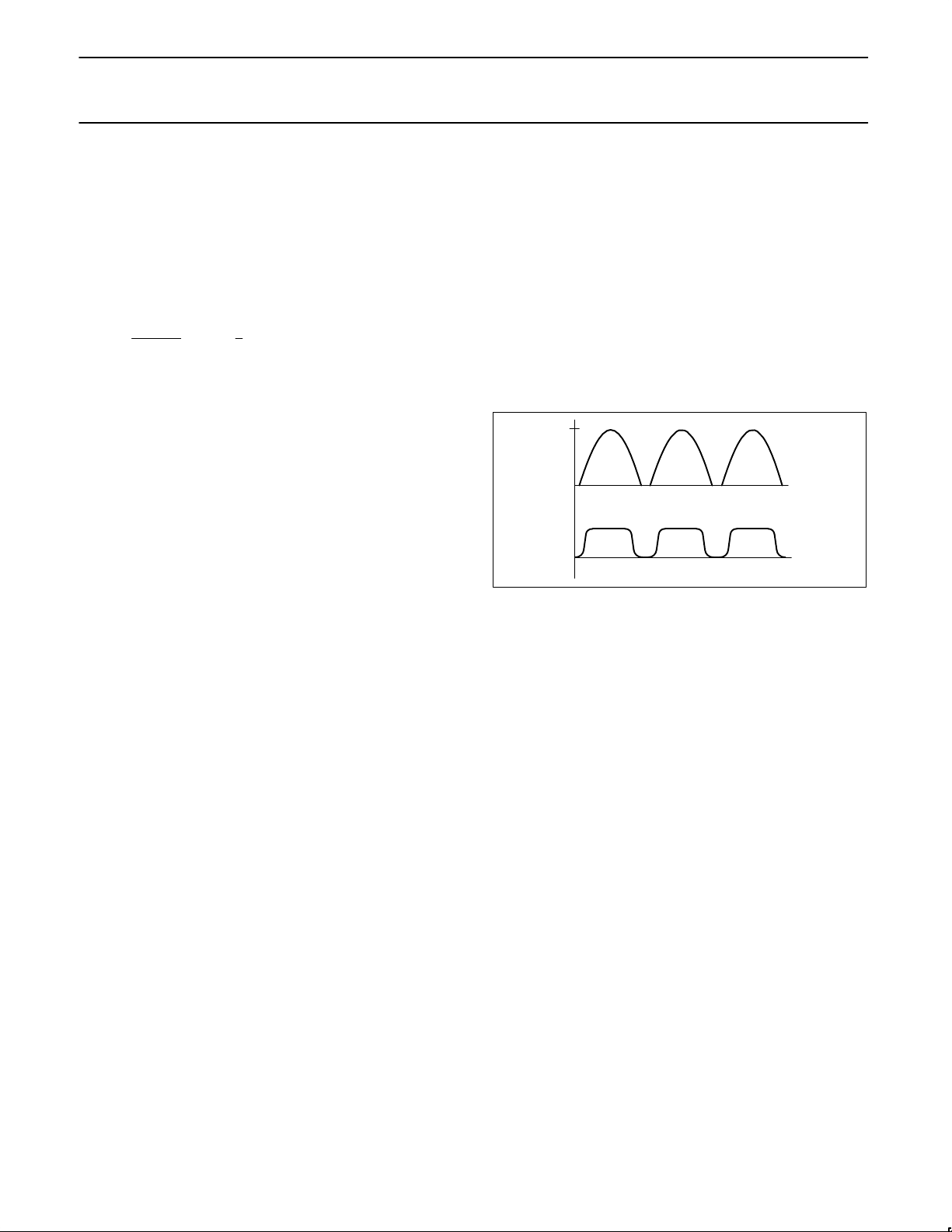
works well in most LED display systems. Waveforms are
shown below:
V
S
I
SEG
The duty cycle for this system depends upon VS, VF and the output
characteristics of the display driver.
With
V
S
= 4.9V peak
V
F
= 2.0V
The duty cycle is approximately 60%.
Page 8
Philips Semiconductors Linear Products Product specification
NE587LED decoder/driver
August 31, 1994
537
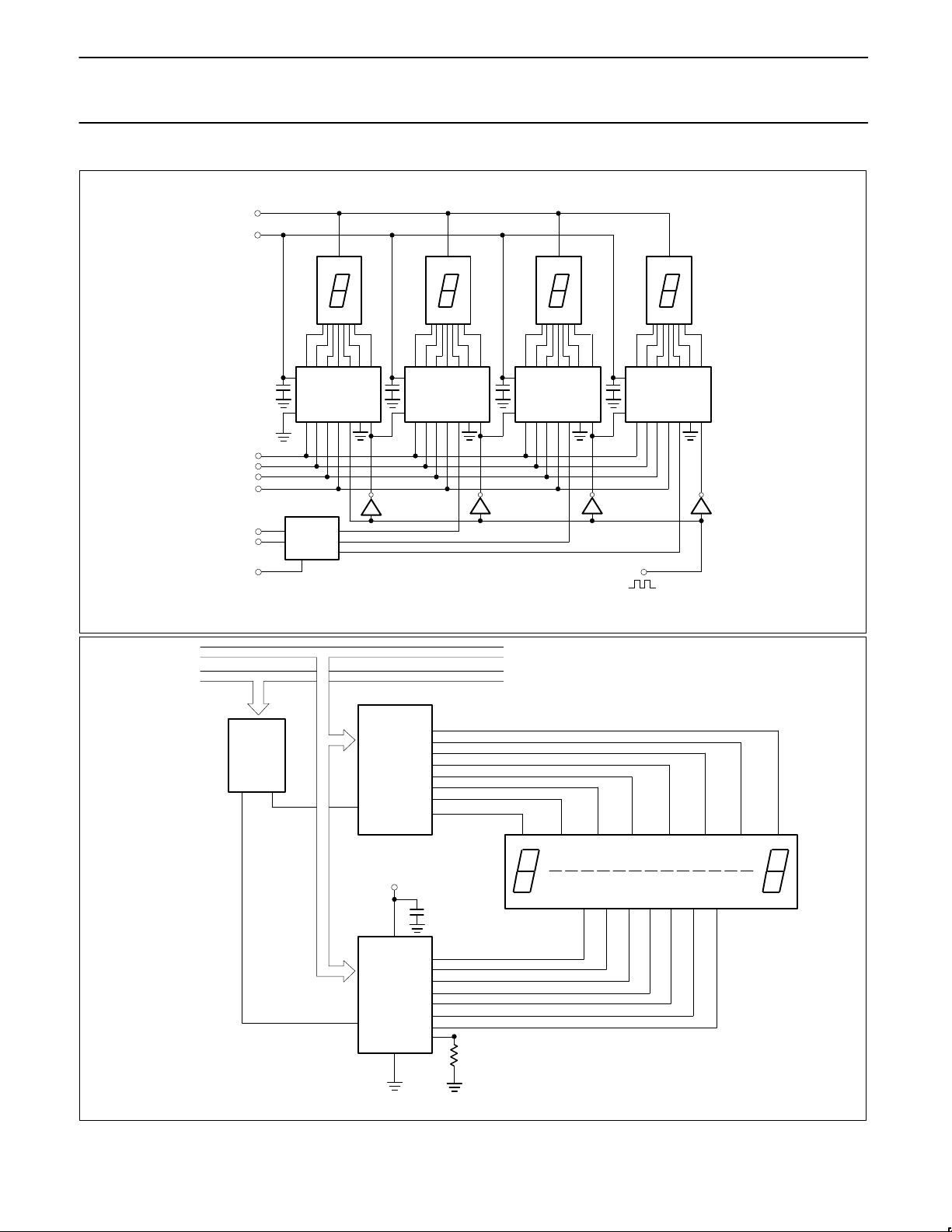
Figure 6. 4-Digit Display with Brightness Control and Leading-Edge Ripple Blanking
V
S
V
CC
D
3
D
2
D
1
D
0
A
0
A
1
LE
BRIGHTNESS CONTROL
NE587
DIGIT
DECODE
NE587 NE587 NE587
Figure 7. Interfacing 8-Digit LED Display with µP Bus
NE587
V
CC
D
0
NE591
ADDRESS
DECODE
DATA BUS
ADDRESS BUS
a b c d e f g
D
1D2D3
D4D5D6D
7
R
P
.01µF
Page 9
Philips Semiconductors Linear Products Product specification
NE587LED decoder/driver
August 31, 1994
538
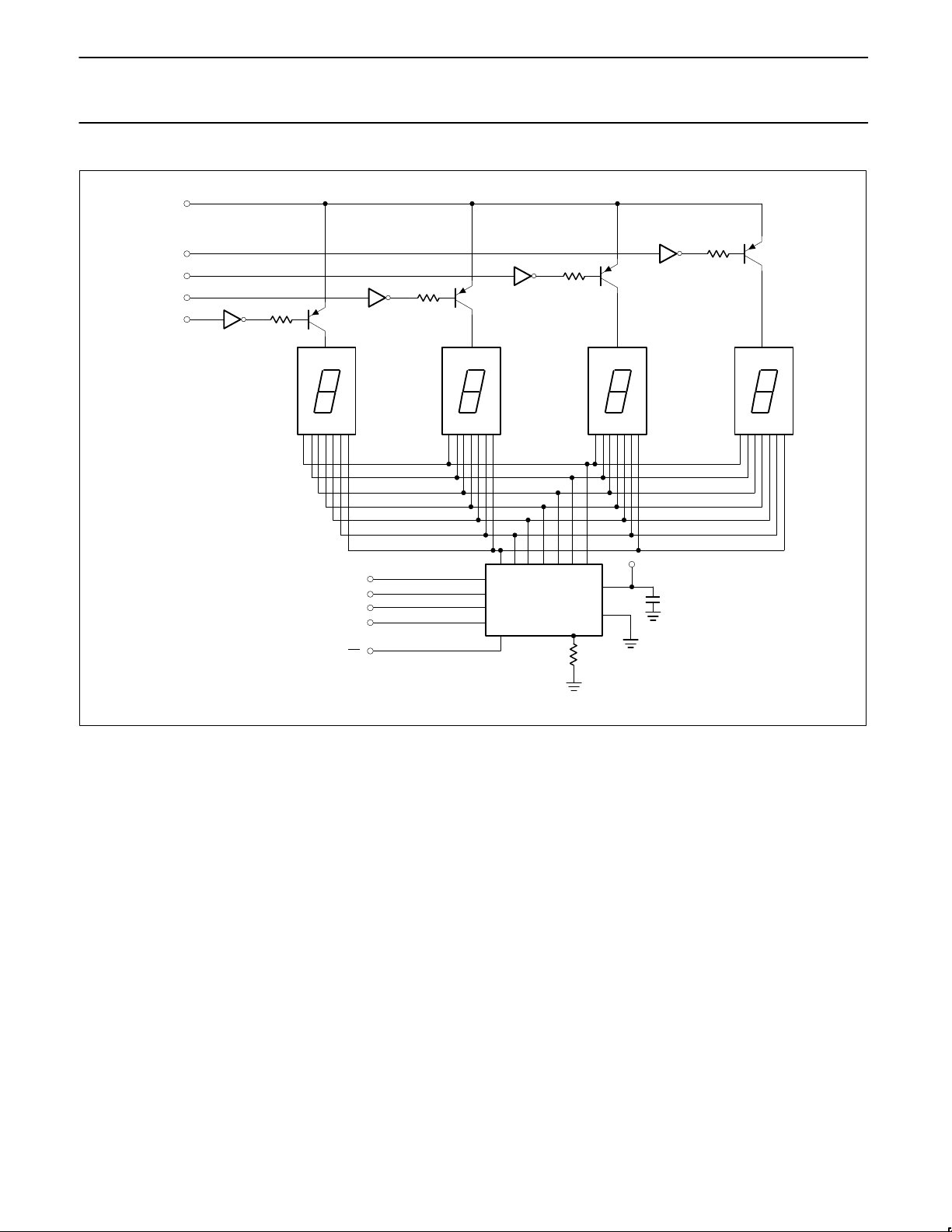
Figure 8. Interfacing 4-Digit Multiplexed LED Display
V
S
DIGIT 1
DIGIT 2
DIGIT 3
DIGIT 4
NE587
V
CC
R
P
D
3
D
2
D
1
D
0
LE
 Loading...