

Page 1

Philips Semiconductors Product specification
NE5592Video amplifier
DESCRIPTION
The NE5592 is a dual monolithic, two-stage, differential output,
wideband video amplifier. It offers a fixed gain of 400 without
external components and an adjustable gain from 400 to 0 with one
external resistor. The input stage has been designed so that with the
addition of a few external reactive elements between the gain select
terminals, the circuit can function as a high-pass, low-pass, or
band-pass filter. This feature makes the circuit ideal for use as a
video or pulse amplifier in communications, magnetic memories,
display, video recorder systems, and floppy disk head amplifiers.
FEATURES
•110MHz unity gain bandwidth
•Adjustable gain from 0 to 400
•Adjustable pass band
•No frequency compensation required
•Wave shaping with minimal external components
PIN CONFIGURA TION
D, N Packages
1
IN A
1
2
IN A
2
3
G
A
4
G
A
5
V
EE
OUT B
OUT B
6
1
78
2
Figure 1. Pin Configuration
APPLICATIONS
•Floppy disk head amplifier
•Video amplifier
•Pulse amplifier in communications
•Magnetic memory
•Video recorder systems
14
OUT A
2
13
A
B
OUT A
1
12
V
CC
11
G
B
10
G
B
9
IN B
2
IN B
1
SL00582
ORDERING INFORMATION
DESCRIPTION TEMPERATURE RANGE ORDER CODE DWG #
14-Pin Plastic Dual In-Line Package (DIP) 0 to 70°C NE5592N SOT27-1
14-Pin Small Outline (SO) package 0 to 70°C NE5592D SOT108-1
EQUIVALENT CIRCUIT
+V
INPUT 1
R
Q
1
G
Q7AQ
R
1
R
R
4
7A
2
INPUT 2
Q
2
R
6
7B
R
7B
R
8
Q
4
G
R
1
R
15
Figure 2. Equivalent Circuit
R
R
9
10
Q
6
Q
5
Q
3
R
11
R
12
Q
9
R
16
Q
10
R
13
OUTPUT 1
OUTPUT 2
Q
11
R
14
–V
SL00583
1987 Oct 20 853-0888 91020
2
Page 2

Philips Semiconductors Product specification
SYMBOL
PARAMETER
TEST CONDITIONS
UNITS
NE5592Video amplifier
ABSOLUTE MAXIMUM RATINGS
TA=25°C, unless otherwise specified.
SYMBOL
V
CC
V
IN
V
CM
I
OUT
T
A
T
STG
P
D MAX
Supply voltage ±8 V
Differential input voltage ±5 V
Common mode Input voltage ±6 V
Output current 10 mA
Operating temperature range
NE5592
Storage temperature range -65 to +150 °C
Maximum power dissipation,
TA=25°C (still air)
D package 1.03 W
N package 1.48 W
NOTES:
1. Derate above 25°C at the following rates:
D package 8.3mW/°C
N package 11.9mW/°C
PARAMETER RATING UNIT
0 to +70 °C
1
DC ELECTRICAL CHARACTERISTICS
TA=+25°C, VSS=±6V, VCM=0, unless otherwise specified. Recommended operating supply voltage is V
connected together.
A
R
C
I
OS
I
BIAS
VOL
IN
IN
Differential voltage gain RL=2kΩ, V
OUT
=3V
P-P
Input resistance 3 14 kΩ
Input capacitance 2.5 pF
Input offset current 0.3 3 µA
Input bias current 5 20 µA
Input noise voltage BW 1kHz to 10MHz 4 nV/√Hz
V
IN
CMRR Common-mode rejection ratio
Input voltage range ±1.0 V
VCM± 1V, f<100kHz
V
± 1V, f=5MHz
CM
PSRR Supply voltage rejection ratio ∆VS= ± 0.5V 50 85 dB
V
=1V
; f=100kHz
P-P
=1kΩ
L
RL=∞
R
=∞
L
RL=∞ 35 44 mA
V
V
V
R
I
OS
CM
OUT
CC
OUT
Channel separation
OUT
(output referenced) R
Output offset voltage
gain select pins open
Output common-mode voltage RL=∞ 2.4 3.1 3.4 V
Output differential voltage swing RL=2kΩ 3.0 4.0 V
Output resistance 20 Ω
Power supply current
(total for both sides)
= ±6.0V , and gain select pins are
S
LIMITS
Min Typ Max
400 480 600 V/V
60 93
87
65 70 dB
0.5
0.25
1.5
0.75
dB
dB
V
V
1987 Oct 20
3
Page 3
Philips Semiconductors Product specification
SYMBOL
PARAMETER
TEST CONDITIONS
UNITS
SYMBOL
PARAMETER
TEST CONDITIONS
UNITS
NE5592Video amplifier
DC ELECTRICAL CHARACTERISTICS
VSS=±6V, VCM=0, 0°C ≤ T
≤ 70°C, unless otherwise specified. Recommended operating supply voltage is V
A
connected together.
A
VOL
R
IN
I
OS
I
BIAS
V
IN
CMRR Common-mode rejection ratio
Differential voltage gain RL=2kΩ, V
OUT
=3V
P-P
Input resistance 1 11 kΩ
Input offset current 5 µA
Input bias current 30 µA
Input voltage range ±1.0 V
VCM± 1V, f<100kHz
R
=φ
S
PSRR Supply voltage rejection ratio ∆VS= ± 0.5V 50 dB
V
=1V
Channel separation
V
OS
Output offset voltage
OUT
(output referenced) R
gain select pins connected
; f=100kHz
P-P
=1kΩ
L
RL=∞ 1.5 V
together
gain select pins open RL=∞ 1.0 V
V
I
OUT
CC
Output differential voltage swing RL=2kΩ 2.8 V
Power supply current
(total for both sides) RL=∞ 47 mA
= ±6.0V , and gain select pins are
S
LIMITS
Min Typ Max
350 430 600 V/V
55 dB
70 dB
AC ELECTRICAL CHARACTERISTICS
TA=+25°C VSS=±6V, VCM=0, unless otherwise specified. Recommended operating supply voltage VS=±6.0V. Gain select pins connected
together.
LIMITS
Min Typ Max
BW Bandwidth V
t
R
t
PD
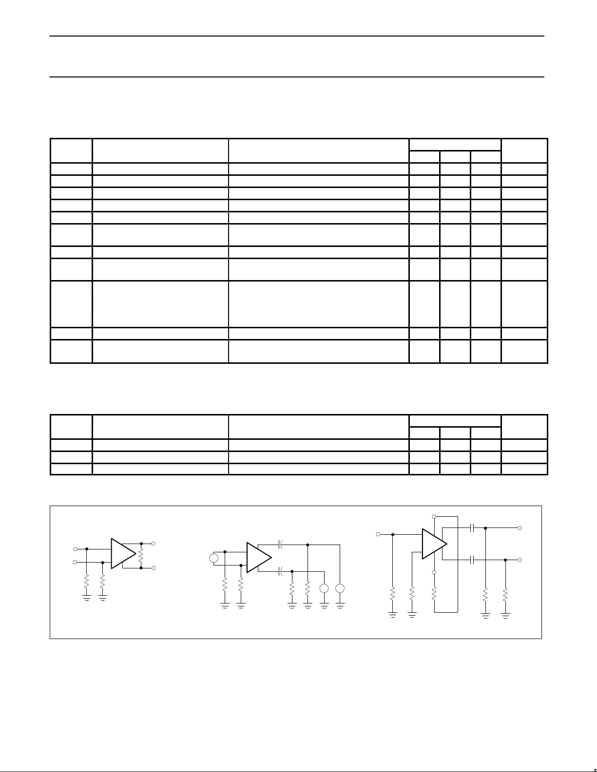
TEST CIRCUITS T
V
Rise time 15 20 ns
Propagation delay V
=25°C unless otherwise specified.
A
0.2µF
IN
5592
51 51
V
R
OUT
L
e
in
51 51
5592
0.2µF
Figure 3. Test Circuits
OUT
OUT
1k 1k
=1V
=1V
P-P
P-P
2,9
1,8
e
OUT
e
OUT
4,10
51 51 1k
V
25 MHz
7.5 12 ns
3,11
13,6
5592
= ±6V TA = 25°C
S
0.2µF
14,7
R
adj
0.2µF
1k
SL00584
1987 Oct 20
4
Page 4
Philips Semiconductors Product specification
NE5592Video amplifier
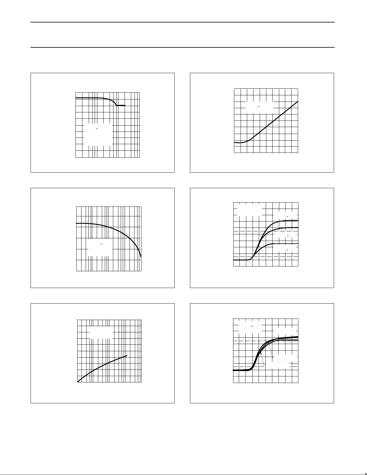
TYPICAL PERFORMANCE CHARACTERISTICS
Common-Mode Rejection Ratio as a Function of Frequency
100
90
80
70
60
50
Vs = + 6V
COMMON MODE REJECTION RATIO —dB
40
30
20
10
0
T
R
V
5
10
FREQUENCY — Hz
= 25oC
A
= 0
S
= 2V p-p
IN
6
10
7
10
8
10
SL00585
Figure 4.
Output Voltage Swing as a Function of Frequency
6
5
p-p
4
3
2
OUTPUT VOLTAGE—V
1
Vs = + 6V
= 1kΩ
R
L
TA = 25oC
Differential Overdrive Recovery Time
50
45
40
35
30
25
20
15
10
5
OVERDRIVE RECOVERY TIME—ns
0
Vs = + 6V
= 25oC
T
A
0 40 80 120 160 200
DIFFERENTIAL INPUT VOLTAGE—mV
Figure 7.
Pulse Response as a Function of Supply Voltage
RL = 1kΩ
1.6
1.4
1.2
0.8
0.6
0.4
OUTPUT VOLTAGE—V
0.2
= 25oC
T
A
1
0
Vs = + 8V
Vs = + 6V
Vs = + 3V
SL00588
0
10410
5
6
10
FREQUENCY — Hz
10710
8
Figure 5.
Channel Separation as a Function of Frequency
0
–10
–20
–30
–40
–50
–60
–70
CHANNEL SEPARATON—dB
–80
–90
10510
RL = 1kΩ
= 25oC
T
A
6
7
10
FREQUENCY — Hz
8
10
9
10
Figure 6.
SL00586
SL00587
–15–10 –5 0 5 10 15 20 25 30 35
TIME—nS
Figure 8.
Pulse Response as a Function of Temperature
1.6
Vs = + 6V
1.4
1.2
1
0.8
0.6
0.4
0.2
0
OUTPUT VOLTAGE—V
–0.2
–0.4
= 1kΩ
R
L
–15–10 –5 0 5 10 15 20 25 30 35
TIME—nS
TA = 0oC
TA = 25oC
TA = 70oC
Figure 9.
SL00589
SL00590
1987 Oct 20
5
Page 5
Philips Semiconductors Product specification
NE5592Video amplifier
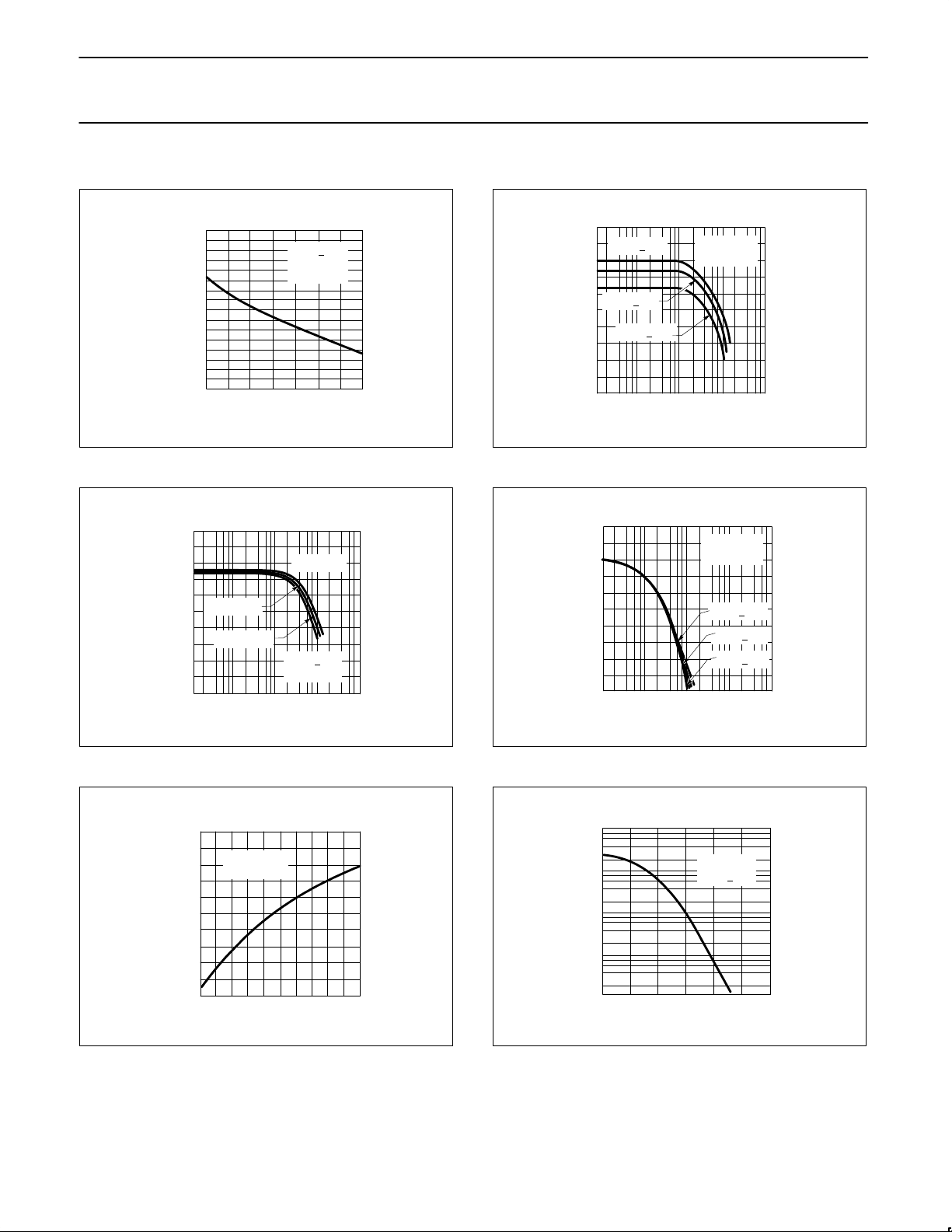
TYPICAL PERFORMANCE CHARACTERISTICS (Continued)
Voltage Gain as a Function of Temperature
1.6
30 40
Vs = + 6V
= 1kΩ
R
L
f = 1MHz
50
60
70
1.2
0.8
0.4
0
–0.4
–0.8
–1.2
RELATIVE VOLTAGE GAIN—dB
–1.6
0
20
10
TEMPERATURE: °C
Figure 10.
Gain vs Frequency as a Function of Temperature
60
7
10
TA = 0oC
Vs = + 6V
= 1kΩ
R
L
10
8
9
10
50
40
TA = 25oC
30
TA = 70oC
VOLTAGE GAIN—dB
20
10
10510
6
FREQUENCY — Hz
Figure 11.
SL00591
SL00592
Gain vs Frequency as a Function of Supply Voltage
60
VS = +8V
50
40
VS = +6V
30
VS = +3V
VOLTAGE GAIN—dB
20
10
5
10
10610710
fFREQUENCY—Hz
TA = 25oC
= 1kΩ
R
L
8
9
10
SL00594
Figure 13.
Phase vs Frequency as a Function of Supply Voltage
7
TA = 25oC
= 1kΩ
R
L
VS = +8V
VS = +6V
VS = +3V
8
10
9
10
SL00595
0
30
60
90
120
150
180
PHASE SHIFT – DEGREES
210
240
5
10610
10
fFREQUENCY—Hz
Figure 14.
Voltage Gain as a Function of Supply Voltage
1987 Oct 20
4
3
F = 100kHz
2
1
0
–1
–2
–3
VOLTAGE GAIN—dB
–4
–5
–6
= 25oC
T
A
345678
SUPPLY VOLTAGE—V
Figure 12.
SL00593
Voltage Gain as a Function of R
3
10
R
ADJ
4
10
– OHMS
TA = 25oC
R
L
2
10
10
VOLTAGE GAIN
1
–
10
1
11010210
= +6V
3
ADJ
10510
6
SL00596
Figure 15.
6
Page 6
Philips Semiconductors Product specification
NE5592Video amplifier
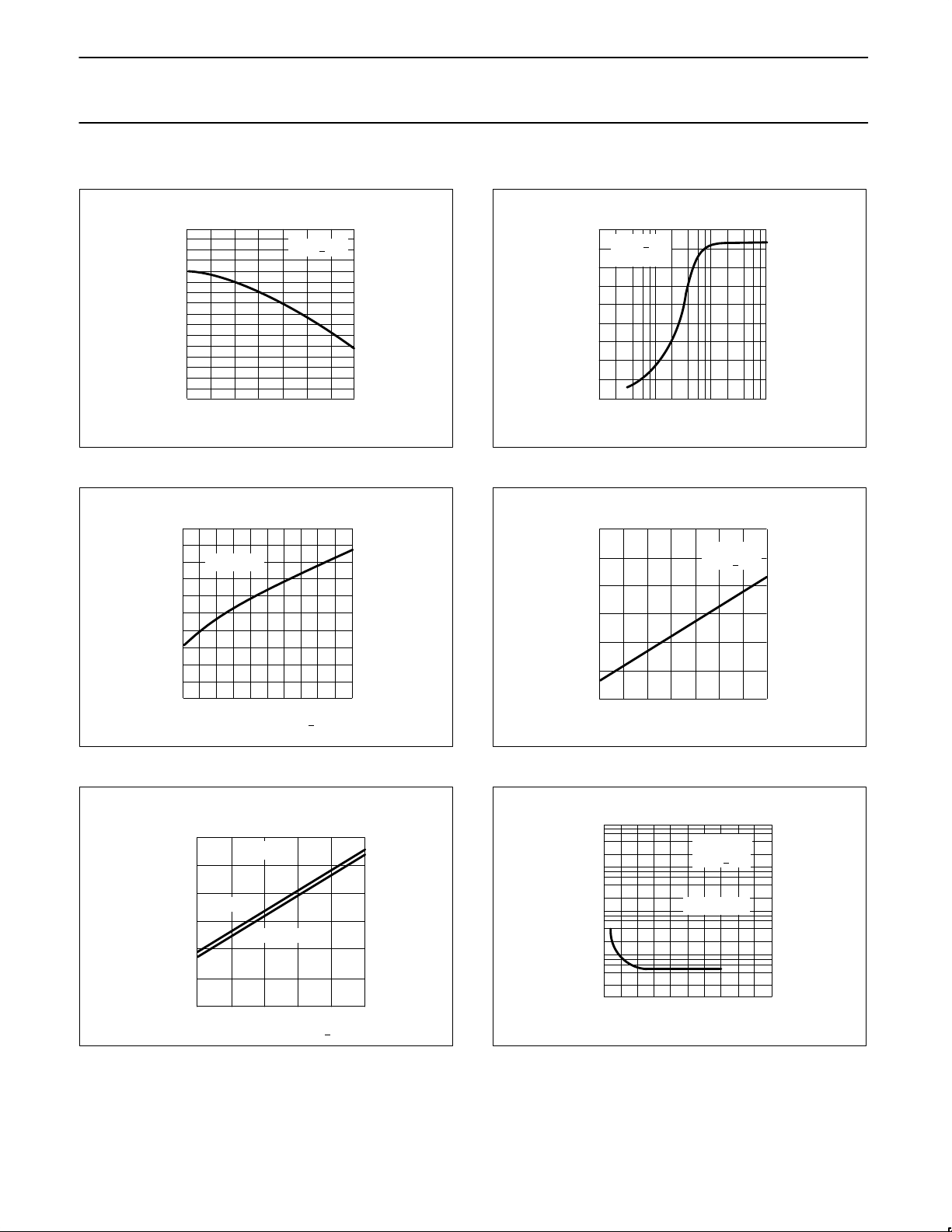
TYPICAL PERFORMANCE CHARACTERISTICS (Continued)
Supply Current as a Function of Temperature
35
VS = +6V
34
33
SUPPLY CURRENT—mA
32
010203040506070
TEMPERATURE –
o
C
Figure 16.
Supply Current as a Function of Supply Voltage
50
40
TA = 25oC
30
20
SUPPLY CURRENT—mA
10
SL00597
Output Voltage Swing as a Function of Load Resistance
VS = +6V
4
p–p
TA = 2oC
3
2
1
OUTPUT VOLTAGE SWING-V
0
5
10
6
10
LOAD RESISTANCE – OHMS
7
10
8
10
SL00600
Figure 19.
Input Resistance as a Function of Temperature
25
Ω
20
15
INPUT RESISTANCE – k
GAIN 1
= +6V
V
S
0
3456 78
SUPPLY VOLTAGE – +
V
Figure 17.
Output Voltage Swing and Sink Current as a
Function of Supply Voltage
6
P
5
4
3
2
1
OUTPUT SINK CURRENT-mA
OUTPUT VOLTAGE SWING—V
0
T
= 25oC
A
VOLTAGE
CURRENT
3456 78
SUPPLY VOLTAGE – +V
Figure 18.
SL00598
SL00599
10
010 203040 506070
TEMPERATURE – oC
Figure 20.
Input Noise Voltage as a Function of Frequency
____
√
1000
100
10
INPUT NOISE VOLTAGE – nV/ Hz
1
1
2
10
TA = 25oC
VS = +6V
RS = 100Ω
6
4
10
10
FREQUENCY – Hz
10810
10
Figure 21.
SL00601
SL00602
1987 Oct 20
7
 Loading...