

Page 1
Philips Semiconductors RF Communications Products Product specification
NE/SE5539High frequency operational amplifier
229
April 15, 1992 853-0814 06456
DESCRIPTION
The NE/SE5539 is a very wide bandwidth, high slew rate, monolithic
operational amplifier for use in video amplifiers, RF amplifiers, and
extremely high slew rate amplifiers.
Emitter-follower inputs provide a true differential input impedance
device. Proper external compensation will allow design operation
over a wide range of closed-loop gains, both inverting and
non-inverting, to meet specific design requirements.
FEATURES
•Bandwidth
– Unity gain - 350MHz
– Full power - 48MHz
– GBW - 1.2GHz at 17dB
•Slew rate: 600/Vµs
•A
VOL
: 52dB typical
•Low noise - 4nV√Hz typical
•MIL-STD processing available
APPLICATIONS
•High speed datacom
•Video monitors & TV
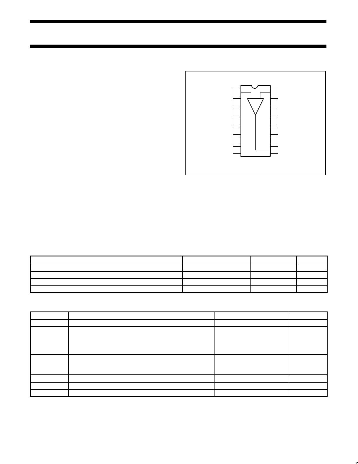
PIN CONFIGURATION
+ INPUT
NC
-V
SUPPLY
- INPUT
NC
NC
NC
V
OS
ADJ
/
A
V
ADJ
GROUND
+V
NC
OUTPUT
D, F, N Packages
NC
1
2
3
4
5
6
7
14
13
12
11
10
9
8
Top View
FREQUENCY
COMPENS.
+ –
•Satellite communications
•Image processing
•RF instrumentation & oscillators
•Magnetic storage
•Military communications
ORDERING INFORMATION
DESCRIPTION TEMPERATURE RANGE ORDER CODE DWG #
14-Pin Plastic Dual In-Line Package (DIP) 0 to +70°C NE5539N 0405B
14-Pin Plastic Small Outline (SO) package 0 to +70°C NE5539D 0175D
14-Pin Ceramic Dual In-Line Package 0 to +70°C NE5539F 0581B
14-Pin Ceramic Dual In-Line Package -55 to +125°C SE5539F 0581B
ABSOLUTE MAXIMUM RATINGS
1
SYMBOL
PARAMETER RATING UNITS
V
CC
Supply voltage ±12 V
P
DMAX
Maximum power dissipation,
T
A
= 25°C (still-air)
2
F package
N package
D package
1.17
1.45
0.99
W
W
W
T
A
Operating temperature range
NE
SE
0 to 70
-55 to +125
°C
°C
T
STG
Storage temperature range -65 to +150 °C
T
J
Max junction temperature 150 °C
T
SOLD
Lead soldering temperature (10sec max) +300 °C
NOTES:
1. Differential input voltage should not exceed 0.25V to prevent excesive input bias current and common-mode voltage 2.5V. These voltage
limits may be exceeded if current is limited to less than 10mA.
2. Derate above 25°C, at the following rates:
F package at 9.3mW/°C
N package at 11.6mW/°C
D package at 7.9mW/°C
Page 2
Philips Semiconductors RF Communications Products Product specification
NE/SE5539High frequency operational amplifier
April 15, 1992
230
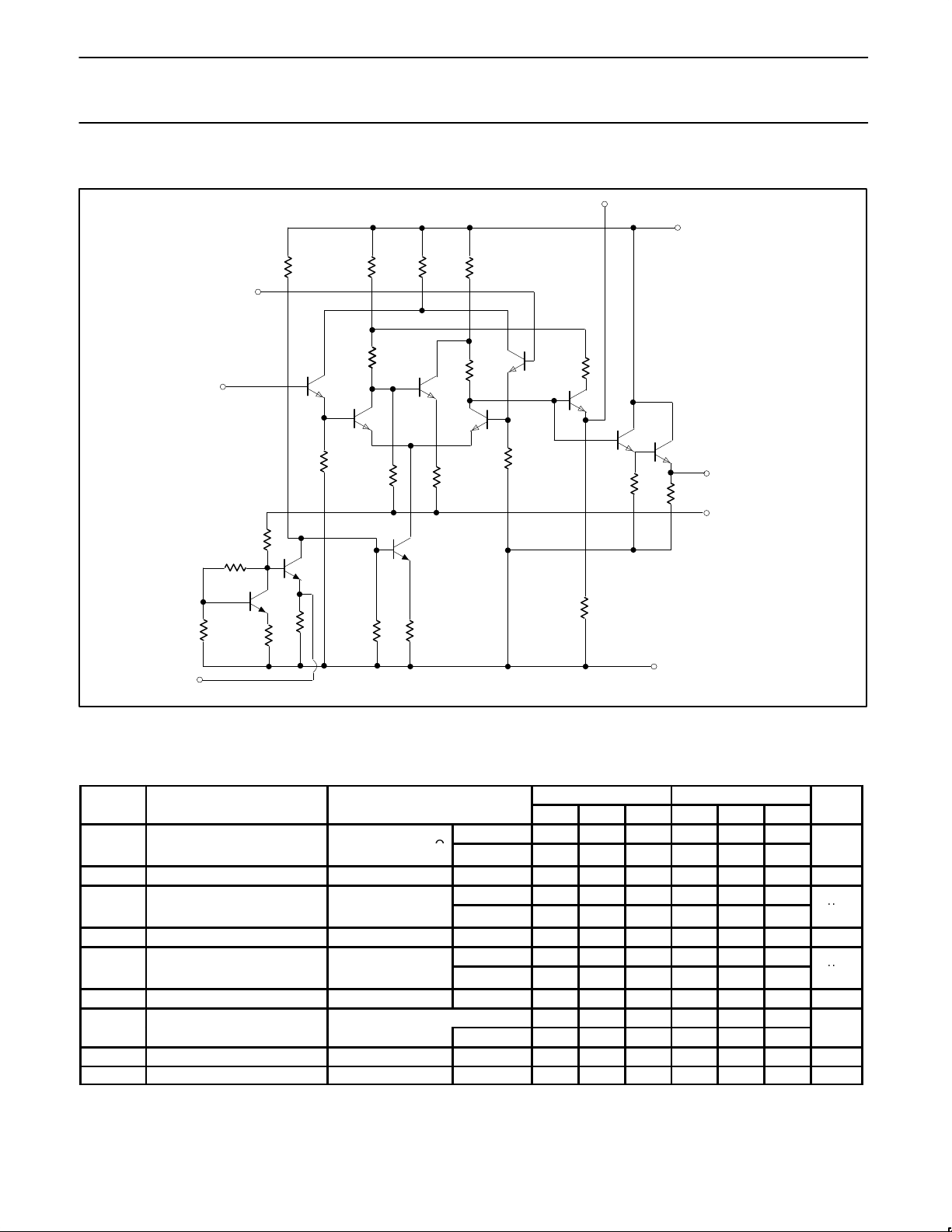
EQUIVALENT CIRCUIT
(–) 14
INVERTING INPUT
(+) 1
NON–INVERTING
INPUT
5
(3) –V
CC
(7) GRD
(8) OUTPUT
(10) +V
CC
(12) FREQUENCY COMP.
2.2k
R
18
R
19
R
3
R
5
R
2
R
6
R
8
Q
1
Q
2
Q
4
Q
3
Q
6
Q
5
Q
7
Q
8
R
20
R
1
R
4
R
21
R
9
R
10
R
7
R
17
R
16
Q
9
Q
10
R
13
R
11
R
12
R
14
R
15
Q
11
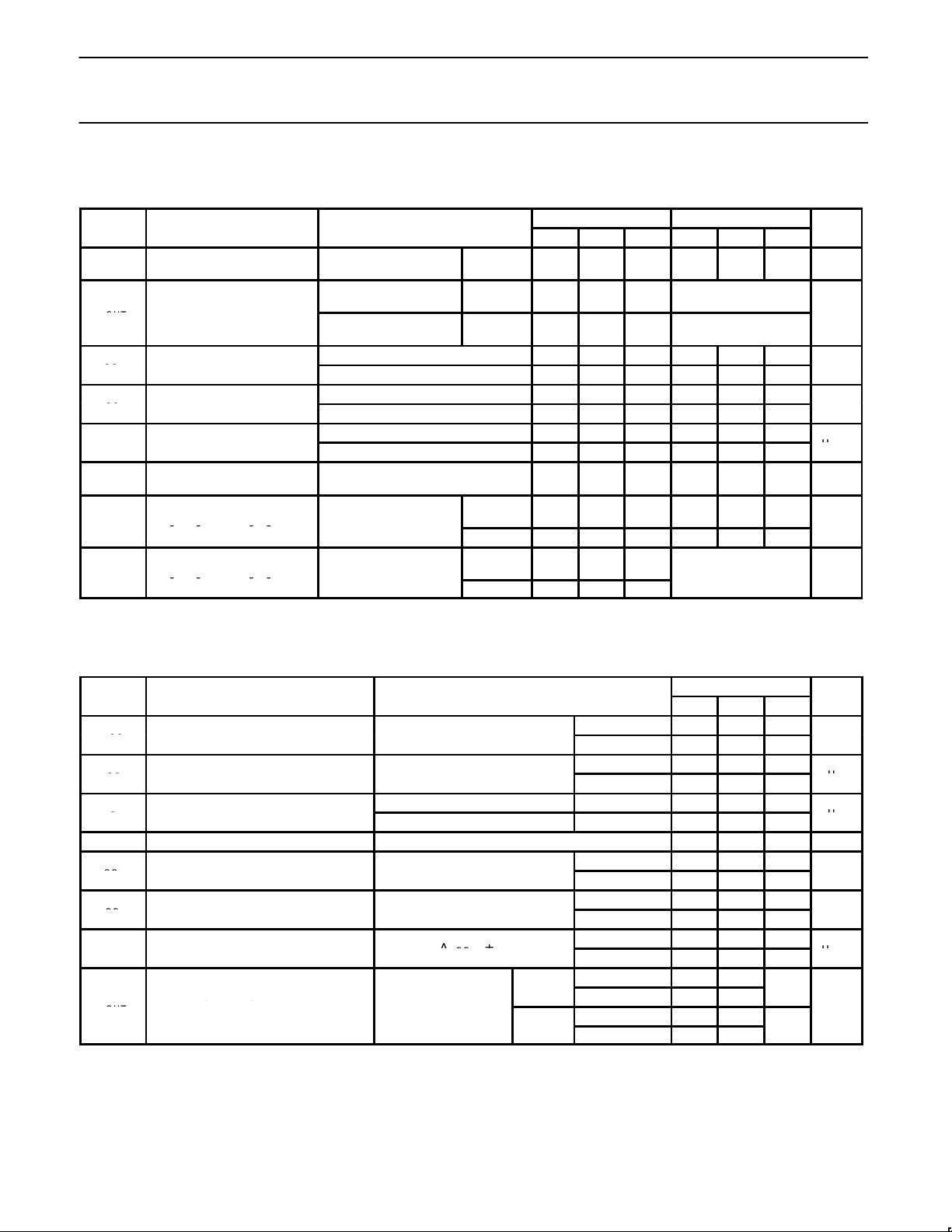
DC ELECTRICAL CHARACTERISTICS
VCC = ±8V, TA = 25°C; unless otherwise specified.
SE5539 NE5539
SYMBOL
PARAMETER
TEST CONDITIONS
MIN TYP MAX MIN TYP MAX
UNITS
Over temp 2 5
VOSInput offset voltage
VO = 0V, RS = 100Ω
TA = 25°C
2 3 2.5 5
mV
∆VOS/∆T 5 5 µV/°C
Over temp 0.1 3
IOSInput offset current
TA = 25°C
0.1 1 2
µA
∆IOS/∆T 0.5 0.5 nA/°C
Over temp 6 25
IBInput bias current
TA = 25°C
5 13 5 20
µA
∆IB/∆T 10 10 nA/°C
F = 1kHz, RS = 100Ω, VCM ±1.7V 70 80 70 80
CMRR
Common mode rejection ratio
Over temp 70 80
dB
R
IN
Input impedance 100 100 kΩ
R
OUT
Output impedance 10 10 Ω
Page 3
Philips Semiconductors RF Communications Products Product specification
NE/SE5539High frequency operational amplifier
April 15, 1992
231
DC ELECTRICAL CHARACTERISTICS (Continued)
VCC = ±8V, TA = 25°C; unless otherwise specified.
SE5539 NE5539
SYMBOL
PARAMETER
TEST CONDITIONS
MIN TYP MAX MIN TYP MAX
UNITS
V
OUT
Output voltage swing
RL = 150Ω to GND and
470Ω to -V
CC
+Swing
-Swing
+2.3
-1.7
+2.7
-2.2
V
RL = 25Ω to GND
Over temp
+Swing
-Swing
+2.3
-1.5
+3.0
-2.1
V
OUT
Output voltage swing
RL = 25Ω to GND
T
A
= 25°C
+Swing
-Swing
+2.5
-2.0
+3.1
-2.7
V
VO = 0, R1 = ∞, Over temp 14 18
I
CC+
Positive supply current
VO = 0, R1 = ∞, TA = 25°C 14 17 14 18
mA
VO = 0, R1 = ∞, Over temp 11 15
I
CC-
Negative supply current
VO = 0, R1 = ∞, TA = 25°C 11 14 11 15
mA
∆VCC = ±1V, Over temp 300 1000
PSRR
Power supply rejection ratio
∆VCC = ±1V, TA = 25°C 200 1000
µV/V
A
VOL
Large signal voltage gain
VO = +2.3V, -1.7V, RL = 150Ω to
GND, 470Ω to -V
CC
47 52 57 dB
VOL
VO = +2.3V, -1.7V
Over
temp
A
VOL
Large signal voltage gain
RL = 2Ω to GND TA = 25°C 47 52 57
dB
VOL
VO = +2.5V, -2.0V
Over
temp
46 60
A
VOL
Large signal voltage gain
RL = 2Ω to GND TA = 25°C 48 53 58
dB
DC ELECTRICAL CHARACTERISTICS
VCC = ±6V, TA = 25°C; unless otherwise specified.
SE5539
SYMBOL
PARAMETER
TEST CONDITIONS
MIN TYP MAX
UNITS
Over temp 2 5
VOSInput offset voltage
TA = 25°C 2 3
mV
Over temp 0.1 3
IOSInput offset current
TA = 25°C 0.1 1
µA
Over temp 5 20
IBInput bias current
TA = 25°C 4 10
µA
CMRR Common-mode rejection ratio VCM = ±1.3V, RS = 100Ω 70 85 dB
Over temp 11 14
I
CC+
Positive supply current
TA = 25°C 11 13
mA
Over temp 8 11
I
CC-
Negative supply current
TA = 25°CmA 8 10
mA
Over temp 300 1000
PSRR
Power supply rejection ratio
∆VCC = ±1V
TA = 25°C
µV/V
Over +Swing +1.4 +2.0
RL = 150Ω to GND temp –Swing –1.1 –1.7
V
OUT
Output voltage swing
and 390Ω to –V
CC
TA = +Swing +1.5 +2.0
V
25°C –Swing –1.4 –1.8
A
A
Large signal voltage gain
Large signal voltage gain
dB
dB
Page 4

Philips Semiconductors RF Communications Products Product specification
NE/SE5539High frequency operational amplifier
April 15, 1992
232
AC ELECTRICAL CHARACTERISTICS
VCC = ±8V, RL = 150Ω to GND and 470Ω to -VCC, unless otherwise specified.
SE5539 NE5539
SYMBOL
PARAMETER
TEST CONDITIONS
MIN TYP MAX MIN TYP MAX
UNITS
BW Gain bandwidth product ACL = 7, VO = 0.1 V
P-P
1200 1200 MHz
Small signal bandwidth ACL = 2, RL = 150Ω
1
110 110 MHz
t
S
Settling time ACL = 2, RL = 150Ω
1
15 15 ns
SR Slew rate ACL = 2, RL = 150Ω
1
600 600 V/µs
t
PD
Propagation delay ACL = 2, RL = 150Ω
1
7 7 ns
Full power response ACL = 2, RL = 150Ω
1
48 48 MHz
Full power response AV = 7, RL = 150Ω
1
20 20 MHz
Input noise voltage RS = 50Ω, 1MHz 4 4 nV/√Hz
Input noise current 1MHz 6 6 pA/√Hz
NOTES:
1. External compensation.
AC ELECTRICAL CHARACTERISTICS
VCC = ±6V, RL = 150Ω to GND and 390Ω to -VCC, unless otherwise specified.
SE5539
SYMBOL
PARAMETER
TEST CONDITIONS
MIN TYP MAX
UNITS
Gain bandwidth product ACL = 7 700
BW
Small signal bandwidth ACL = 2
1
120
MHz
t
S
Settling time ACL = 2
1
23 ns
SR Slew rate ACL = 2
1
330 V/µs
t
PD
Propagation delay ACL = 2
1
4.5 ns
Full power response ACL = 2
1
20 MHz
NOTES:
1. External compensation.
TYPICAL PERFORMANCE CURVES
NE5539 Open-Loop Phase NE5539 Open-Loop Gain
0
90
180
270
360
1 MHz 10MHz 100MHz 1GHz
FREQUENCY (Hz)
PHASE (DEG)
60
50
40
30
20
10
0
1 MHz 10MHz 100MHz 1GHz
FREQUENCY (Hz)
GAIN (dB)
Page 5

Philips Semiconductors RF Communications Products Product specification
NE/SE5539High frequency operational amplifier
April 15, 1992
233
TYPICAL PERFORMANCE CURVES (Continued)
dB BELOW REF
Power Bandwidth (SE) Power Bandwidth (NE)
SE5539 Open-Loop Gain vs Frequency Power Bandwidth
SE5539 Open-Loop Phase vs Frequency Gain Bandwidth Product vs Frequency
5
4
3
2
1
GAIN (—2)
V
CC
= +8V
R
L
= 2kΩ
3dB B.W
1 MHz 10MHz 100MHz 300Mhz
p–p OUTPUT (V)
FREQUENCY (Hz)
3dB B.W.
1 MHz 10MHz 100MHz 300Mhz
FREQUENCY (Hz)
p–p OUTPUT (V)
4
3
2
1
0
VCC = +6V
R
L
= 150kΩ
GAIN (—2)
1 MHz 10MHz 100MHz 300Mhz
FREQUENCY (Hz)
VCC = +6V
R
L
= 126Ω
0
o
50
40
30
20
10
GAIN (dB)
22
20
18
16
14
12
1MHz 10MHz 100MHz
FREQUENCY (Hz)
GAIN (dB)
3dB BANDWIDTH
3dB BANDWIDTH
AV = X7.5
AV = X10
VCC = ±6V
RL = 150Ω
300MHz
1MHz 10MHz 100MHz
FREQUENCY (Hz)
300MHz
GAIN (–7)
RL = 150Ω
REF
3.04V
P-P
–2
–4
–6
–8
–10
–12
1MHz 10MHz 100MHz
FREQUENCY (Hz)
300MHz
VCC = ±6V
RL = 126Ω
PHASE (DEG)
0°
45°
90°
135°
180°
NOTE:
Indicates typical
distribution –55°C ≤ T
A
≤ 125°C
Page 6

Philips Semiconductors RF Communications Products Product specification
NE/SE5539High frequency operational amplifier
April 15, 1992
234
CIRCUIT LAYOUT CONSIDERATIONS
As may be expected for an ultra-high frequency, wide-gain
bandwidth amplifier, the physical circuit is extremely critical.
Bread-boarding is not recommended. A double-sided copper-clad
printed circuit board will result in more favorable system operation.
An example utilizing a 28dB non-inverting amp is shown in Figure 1.
R5 = 20k TRIMPOT (CERMET)
R
F
= 1.5k (28dB GAIN)
R
6
= 470Ω 5% CARBON
RFC 3T # 26 BUSS WIRE ON
FERROXCUBE VK 200 09/3B CORE
BYPASS CAPACITORS
1nF CERAMIC
(MEPCO OR EQUIV.)
Component Side
(Component Layout)
Bottom Plane
Copper
1
R
5
R
1
R
2
V
IN
R
6
C
C
R
F
R
5
—V
RFC
R
4
RFC
X
X
X
X
X X
X
X
X X
X
X
(1)
+V
OPTIONAL
OFFSET
ADJ.
+V –V
R
5
R
4
R
1
75
R
F
+V
RFC
–14
10
8
3
7
NE5539
1nF
1nF
R
3
75
V
OUT
75
Ω
TERM
470
R
6
RFC
1nF
1nF
—V
V
IN
R
2
+1
75
Figure 1. 28dB Non-Inverting Amp Sample PC Layout
R1 = 75Ω 5% CARBON
R
2
= 75Ω 5% CARBON
R
3
= 75Ω 5% CARBON
R
4
= 36K 5% CARBON
Top Plane Copper
1
(Component Side)
Page 7

Philips Semiconductors RF Communications Products Product specification
NE/SE5539High frequency operational amplifier
April 15, 1992
235
NE5539 COLOR VIDEO AMPLIFIER
The NE5539 wideband operational amplifier is easily adapted for
use as a color video amplifier. A typical circuit is shown in Figure 2
along with vector-scope1 photographs showing the amplifier
differential gain and phase response to a standard five-step
modulated staircase linearity signal (Figures 3, 4 and 5). As can be
seen in Figure 4, the gain varies less than 0.5% from the bottom to
the top of the staircase. The maximum differential phase shown in
Figure 5 is approximately +0.1°.
The amplifier circuit was optimized for a 75Ω input and output
termionation impedance with a gain of approximately 10 (20dB).
NOTE:
1. The input signal was 200mV and the output 2V . V
CC
was ±8V.
7
75
750
—V
22nF
14
—
10
8
3
1
+
75
V
IN
—V
22nF
470
75
—V
Z
O
= 75Ω
1
6dB LOSS—1
75
Figure 2. NE5539 Video Amplifier
Figure 3. Input Signal Figure 4. Differential Gain <0.5%
NOTE:
Instruments used for these measurements were Tektronix 146 NTSC test signal generator, 520A NTSC vectorscope, and 1480 waveform
monitor.
Page 8

Philips Semiconductors RF Communications Products Product specification
NE/SE5539High frequency operational amplifier
April 15, 1992
236
Figure 5. Differential Gain +0.1
o
ZIN = 500
Ω
820
220
2–10pF
+
1
+2V
–8V
470
8
NE5539
118
87
Z
O
= 50
Ω
14
1K
2K
C
LEAD
≈ 1.5pF
Figure 6. Non-Inverting Follower
–
Figure 7. Inverting Follower
+
1
+8V
–8V
470
8
NE5539
118
87
14
3.3pF
1K
320
2–20pF
50
1K
–
 Loading...