

Page 1

RF COMMUNICATIONS PRODUCTS
NE/SE5539
High frequency operational amplifier
Product specification April 15, 1992
IC11
Philips Semiconductors
Page 2
Philips Semiconductors Product specification
NE/SE5539High frequency operational amplifier
DESCRIPTION
The NE/SE5539 is a very wide bandwidth, high slew rate, monolithic
operational amplifier for use in video amplifiers, RF amplifiers, and
extremely high slew rate amplifiers.
Emitter-follower inputs provide a true differential input impedance
device. Proper external compensation will allow design operation
over a wide range of closed-loop gains, both inverting and
non-inverting, to meet specific design requirements.
FEA TURES
•Bandwidth
– Unity gain - 350MHz
– Full power - 48MHz
– GBW - 1.2GHz at 17dB
•Slew rate: 600/Vµs
•A
: 52dB typical
VOL
•Low noise - 4nV√Hz typical
•MIL-STD processing available
APPLICA TIONS
•High speed datacom
•Video monitors & TV
PIN CONFIGURA TION
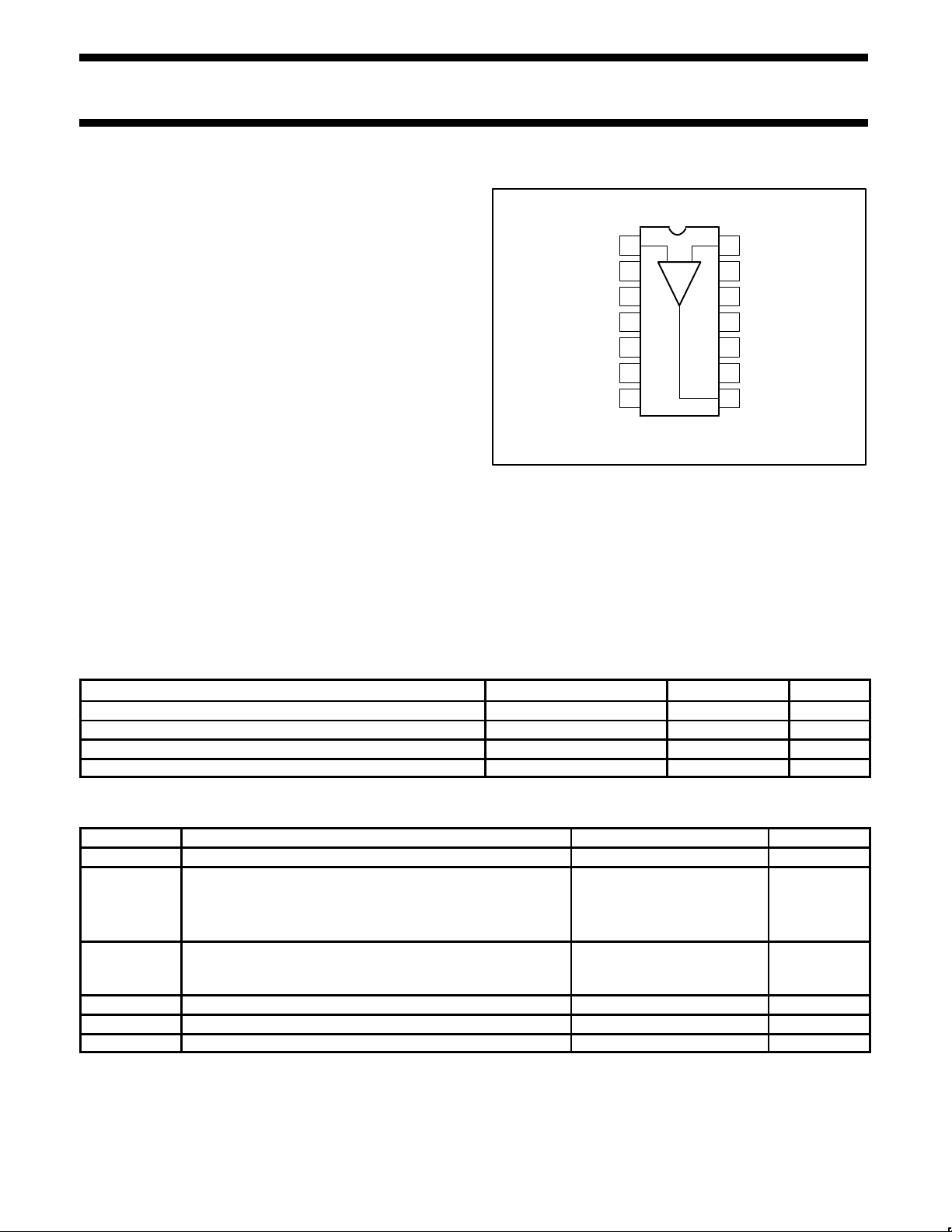
D, F, N Packages
OS
A
V
NC
NC
ADJ
ADJ
NC
1
2
3
4
5
/
6
7
+ INPUT
-V
SUPPLY
V
GROUND
Top View
Figure 1. Pin Configuration
•Satellite communications
•Image processing
•RF instrumentation & oscillators
•Magnetic storage
•Military communications
+–
14
- INPUT
13
NC
FREQUENCY
12
COMPENS.
NC
11
10
+V
9
NC
8
OUTPUT
SL00570
ORDERING INFORMATION
DESCRIPTION TEMPERATURE RANGE ORDER CODE DWG #
14-Pin Plastic Dual In-Line Package (DIP) 0 to +70°C NE5539N SOT27-1
14-Pin Plastic Small Outline (SO) package 0 to +70°C NE5539D SOT108-1
14-Pin Ceramic Dual In-Line Package 0 to +70°C NE5539F 0581B
14-Pin Ceramic Dual In-Line Package -55 to +125°C SE5539F 0581B
ABSOLUTE MAXIMUM RATINGS
SYMBOL
V
CC
P
DMAX
T
A
T
STG
T
J
T
SOLD
NOTES:
1. Differential input voltage should not exceed 0.25V to prevent excesive input bias current and common-mode voltage 2.5V. These voltage
limits may be exceeded if current is limited to less than 10mA.
2. Derate above 25°C, at the following rates:
Supply voltage ±12 V
Maximum power dissipation,
= 25°C (still-air)
T
A
F package
N package
D package
Operating temperature range
NE
SE
Storage temperature range -65 to +150 °C
Max junction temperature 150 °C
Lead soldering temperature (10sec max) +300 °C
F package at 9.3mW/°C
N package at 11.6mW/°C
D package at 7.9mW/°C
1
PARAMETER RATING UNITS
2
1.17
1.45
0.99
0 to 70
-55 to +125
W
W
W
°C
°C
1992 Apr 15 853-0814 06456
2
Page 3
Philips Semiconductors Product specification
SYMBOL
PARAMETER
TEST CONDITIONS
UNITS
CMRR
C
dB
NE/SE5539High frequency operational amplifier
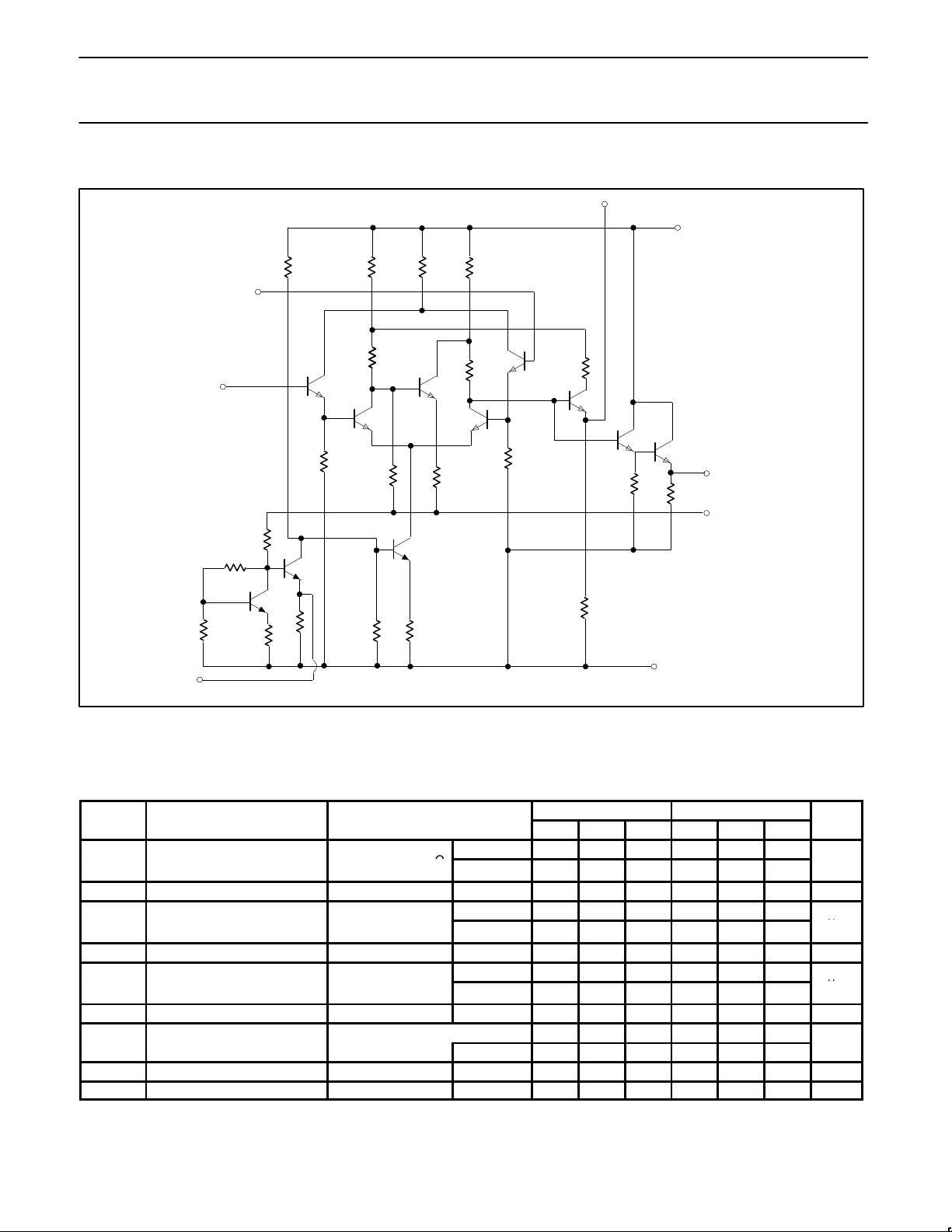
EQUIVALENT CIRCUIT
(12) FREQUENCY COMP.
(10) +V
CC
(–) 14
INVERTING INPUT
(+) 1
NON–INVERTING
INPUT
5
R
18
Q
R
R
13
Q
R
11
R
12
R
14
10
Q
11
R
15
R
R
1
Q
2
20
R
1
R
16
R
19
2
Q
9
R
17
R
3
Q
5
Q
6
R
6
4
Q
3
R
4
R
8
Q
5
Q
7
Q
R
21
R
7
8
R
2.2k
(8) OUTPUT
10
(7) GRD
CC
SL00571
R
9
(3) –V
Figure 2. Equivalent Circuit
DC ELECTRICAL CHARACTERISTICS
VCC = ±8V, TA = 25°C; unless otherwise specified.
V
I
R
R
1992 Apr 15
Input offset voltage VO = 0V, RS = 100Ω
OS
∆VOS/∆T 5 5 µV/°C
Input offset current
OS
∆IOS/∆T 0.5 0.5 nA/°C
I
Input bias current
B
∆IB/∆T 10 10 nA/°C
ommon mode rejection ratio
Input impedance 100 100 kΩ
IN
Output impedance 10 10 Ω
OUT
F = 1kHz, RS = 100Ω, VCM ±1.7V 70 80 70 80
SE5539 NE5539
MIN TYP MAX MIN TYP MAX
Over temp 2 5
TA = 25°C
2 3 2.5 5
Over temp 0.1 3
TA = 25°C
0.1 1 2
Over temp 6 25
TA = 25°C
5 13 5 20
Over temp 70 80
3
mV
µA
µA
Page 4

Philips Semiconductors Product specification
SYMBOL
PARAMETER
TEST CONDITIONS
UNITS
V
Output
V
I
Positi
t
A
I
N
t
A
PSRR
P
V/V
A
VOL
Large signal voltage gain
dB
A
VOL
Large signal voltage gain
dB
SYMBOL
PARAMETER
TEST CONDITIONS
UNITS
VOSI
V
IOSI
t
A
IBI
t
A
I
Positi
t
A
I
N
t
A
PSRR
P
∆V
±1V
V/V
V
Output
V
NE/SE5539High frequency operational amplifier
DC ELECTRICAL CHARACTERISTICS (Continued)
VCC = ±8V, TA = 25°C; unless otherwise specified.
SE5539 NE5539
MIN TYP MAX MIN TYP MAX
V
A
A
A
OUT
OUT
CC+
CC-
VOL
VOL
VOL
Output voltage swing
voltage swing
ve supply curren
egative supply curren
ower supply rejection ratio
Large signal voltage gain
Large signal voltage gain
Large signal voltage gain
RL = 150Ω to GND and
470Ω to -V
CC
RL = 25Ω to GND
Over temp
RL = 25Ω to GND
= 25°C
T
A
VO = 0, R1 = ∞, Over temp 14 18
VO = 0, R1 = ∞, TA = 25°C 14 17 14 18
VO = 0, R1 = ∞, Over temp 11 15
VO = 0, R1 = ∞, TA = 25°C 11 14 11 15
∆VCC = ±1V, Over temp 300 1000
∆VCC = ±1V, TA = 25°C 200 1000
VO = +2.3V , -1.7V, RL = 150Ω to
GND, 470Ω to -V
VO = +2.3V , -1.7V
RL = 2Ω to GND TA = 25°C 47 52 57
VO = +2.5V , -2.0V
RL = 2Ω to GND TA = 25°C 48 53 58
+Swing
-Swing
+Swing
-Swing
+Swing
-Swing
CC
Over
temp
Over
temp
+2.3
+3.0
-1.5
+2.5
-2.0
-2.1
+3.1
-2.7
46 60
+2.3
+2.7
-1.7
-2.2
47 52 57 dB
V
m
m
µ
dB
dB
DC ELECTRICAL CHARACTERISTICS
VCC = ±6V, TA = 25°C; unless otherwise specified.
SE5539
MIN TYP MAX
nput offset voltage
nput offset curren
nput bias curren
CMRR Common-mode rejection ratio VCM = ±1.3V, RS = 100Ω 70 85 dB
CC+
CC-
ve supply curren
egative supply curren
ower supply rejection ratio
CC
=
Over +Swing +1.4 +2.0
OUT
voltage swing
RL = 150Ω to GND temp –Swing –1.1 –1.7
and 390Ω to –V
CC
TA = +Swing +1.5 +2.0
25°C –Swing –1.4 –1.8
Over temp 2 5
TA = 25°C 2 3
Over temp 0.1 3
TA = 25°C 0.1 1
Over temp 5 20
TA = 25°C 4 10
Over temp 11 14
TA = 25°C 11 13
Over temp 8 11
TA = 25°CmA 8 10
Over temp 300 1000
TA = 25°C
m
µ
µ
m
m
µ
1992 Apr 15
4
Page 5

Philips Semiconductors Product specification
SYMBOL
PARAMETER
TEST CONDITIONS
UNITS
SYMBOL
PARAMETER
TEST CONDITIONS
UNITS
BW
MH
NE/SE5539High frequency operational amplifier
AC ELECTRICAL CHARACTERISTICS
VCC = ±8V, RL = 150Ω to GND and 470Ω to -VCC, unless otherwise specified.
SE5539 NE5539
MIN TYP MAX MIN TYP MAX
BW Gain bandwidth product ACL = 7, VO = 0.1 V
Small signal bandwidth ACL = 2, RL = 150Ω
t
Settling time ACL = 2, RL = 150Ω
S
SR Slew rate ACL = 2, RL = 150Ω
t
Propagation delay ACL = 2, RL = 150Ω
PD
Full power response ACL = 2, RL = 150Ω
Full power response AV = 7, RL = 150Ω
P-P
1
1
1
1
1
1
Input noise voltage RS = 50Ω, 1MHz 4 4 nV/√Hz
Input noise current 1MHz 6 6 pA/√Hz
NOTES:
1. External compensation.
AC ELECTRICAL CHARACTERISTICS
VCC = ±6V, RL = 150Ω to GND and 390Ω to -VCC, unless otherwise specified.
Gain bandwidth product ACL = 7 700
Small signal bandwidth ACL = 2
t
Settling time ACL = 2
S
SR Slew rate ACL = 2
t
Propagation delay ACL = 2
PD
Full power response ACL = 2
NOTES:
1. External compensation.
1
1
1
1
1
1200 1200 MHz
110 110 MHz
15 15 ns
600 600 V/µs
7 7 ns
48 48 MHz
20 20 MHz
SE5539
MIN TYP MAX
120
23 ns
330 V/µs
4.5 ns
20 MHz
z
TYPICAL PERFORMANCE CURVES
NE5539 Open-Loop Phase
0
90
180
PHASE (DEG)
270
360
1 MHz 10MHz 100MHz 1GHz
FREQUENCY (Hz)
Figure 3. NE5539 Open-Loop Phase
1992 Apr 15
SL00572
NE5539 Open-Loop Gain
60
50
40
30
GAIN (dB)
20
10
0
1 MHz 10MHz 100MHz 1GHz
FREQUENCY (Hz)
SL00573
Figure 4. NE5539 Open-Loop Gain
5
Page 6

Philips Semiconductors Product specification
NE/SE5539High frequency operational amplifier
TYPICAL PERFORMANCE CURVES (Continued)
Power Bandwidth (SE) Power Bandwidth (NE)
4
5
3
4
3dB B.W
3
p–p OUTPUT (V)
GAIN (—2)
= +8V
V
2
1
CC
= 2kΩ
R
L
1 MHz 10MHz 100MHz 300Mhz
FREQUENCY (Hz)
2
p–p OUTPUT (V)
1
0
1 MHz 10MHz 100MHz 300Mhz
VCC = +6V
= 150kΩ
R
L
GAIN (—2)
3dB B.W.
FREQUENCY (Hz)
SE5539 Open-Loop Gain vs Frequency Power Bandwidth
50
40
30
VCC = +6V
20
GAIN (dB)
10
o
0
1 MHz 10MHz 100MHz 300Mhz
R
= 126Ω
L
FREQUENCY (Hz)
SE5539 Open-Loop Phase vs Frequency Gain Bandwidth Product vs Frequency
0°
45°
90°
PHASE (DEG)
135°
180°
VCC = ±6V
RL = 126Ω
1MHz 10MHz 100MHz
FREQUENCY (Hz)
300MHz
REF
3.04V
P-P
–2
–4
–6
–8
dB BELOW REF
–10
–12
22
20
18
GAIN (dB)
16
14
12
GAIN (–7)
RL = 150Ω
1MHz 10MHz 100MHz
A
= X10
V
AV = X7.5
1MHz 10MHz 100MHz
FREQUENCY (Hz)
3dB BANDWIDTH
3dB BANDWIDTH
FREQUENCY (Hz)
300MHz
VCC = ±6V
RL = 150Ω
300MHz
NOTE:
1992 Apr 15
Indicates typical
distribution –55°C ≤ T
≤ 125°C
A
SL00574
Figure 5. Typical Performance Curves
6
Page 7

Philips Semiconductors Product specification
NE/SE5539High frequency operational amplifier
CIRCUIT LAYOUT CONSIDERATIONS
As may be expected for an ultra-high frequency, wide-gain
bandwidth amplifier, the physical circuit is extremely critical.
OPTIONAL
OFFSET
+V –V
R1 = 75Ω 5% CARBON
= 75Ω 5% CARBON
R
2
R
= 75Ω 5% CARBON
3
= 36K 5% CARBON
R
4
ADJ.
R
5
R
4
R
1
75
V
IN
R
2
75
Bread-boarding is not recommended. A double-sided copper-clad
printed circuit board will result in more favorable system operation.
An example utilizing a 28dB non-inverting amp is shown in Figure 6.
R
F
1nF
+V
RFC
–14
NE5539
7
+1
RFC
—V
R5 = 20k TRIMPOT (CERMET)
R
= 1.5k (28dB GAIN)
F
R6 = 470Ω 5% CARBON
1nF
10
8
470
3
1nF
1nF
75
R
3
R
6
V
OUT
RFC 3T # 26 BUSS WIRE ON
FERROXCUBE VK 200 09/3B CORE
BYPASS CAPACITORS
1nF CERAMIC
(MEPCO OR EQUIV.)
75
TERM
Ω
Top Plane Copper
(Component Side)
1
Component Side
(Component Layout)
—V
RFC
X
R
2
(1)
X
V
IN
XX
X
X
R
5
R
6
R
4
X
X
XX
R
Bottom Plane
X
R
1
+V
X
C
C
RFC
R
F
5
Copper
1
SL00575
Figure 6. 28dB Non-Inverting Amp Sample PC Layout
1992 Apr 15
7
Page 8

Philips Semiconductors Product specification
NE/SE5539High frequency operational amplifier
NE5539 COLOR VIDEO AMPLIFIER
The NE5539 wideband operational amplifier is easily adapted for
use as a color video amplifier. A typical circuit is shown in Figure 7
along with vector-scope1 photographs showing the amplifier
differential gain and phase response to a standard five-step
modulated staircase linearity signal (Figures 8, 9 and 10). As can
be seen in Figure 9, the gain varies less than 0.5% from the bottom
to the top of the staircase. The maximum differential phase shown
in Figure 10 is approximately +0.1°.
The amplifier circuit was optimized for a 75Ω input and output
termionation impedance with a gain of approximately 10 (20dB).
NOTE:
1. The input signal was 200mV and the output 2V . V
750
75
—
V
IN
+
75
—V
22nF
14
10
8
3
7
1
—V
22nF
1
75
470
—V
was ±8V.
CC
6dB LOSS—1
Z
= 75Ω
O
75
SL00578
Figure 9. Differential Gain <0.5%
NOTE:
Instruments used for these measurements were Tektronix 146
NTSC test signal generator, 520A NTSC vectorscope, and 1480
waveform monitor.
Figure 7. NE5539 Video Amplifier
Figure 8. Input Signal
SL00576
SL00577
1992 Apr 15
8
Page 9

Philips Semiconductors Product specification
NE/SE5539High frequency operational amplifier
SL00579
Figure 10. Differential Gain +0.1
o
ZIN = 500
+2V
–8V
1
Ω
820
220
1K
2–10pF
+
NE5539
–
14
C
LEAD
2K
≈ 1.5pF
470
118
8
87
ZO = 50
Ω
SL00580
Figure 11. Non-Inverting Follower
+8V
–8V
1
+
320
2–20pF
1K
50
NE5539
–
14
3.3pF
470
8
1K
118
87
SL00581
Figure 12. Inverting Follower
1992 Apr 15
9
Page 10

Philips Semiconductors Product specification
NE/SE5539High frequency operational amplifier
DIP14: plastic dual in-line package; 14 leads (300 mil) SOT27-1
April 15, 1992
10
Page 11

Philips Semiconductors Product specification
NE/SE5539High frequency operational amplifier
SO14: plastic small outline package; 14 leads; body width 3.9 mm SOT108-1
April 15, 1992
11
Page 12

Philips Semiconductors Product specification
NE/SE5539High frequency operational amplifier
0581B 14-PIN (300 mils wide) CERAMIC DUAL IN-LINE (F) PACKAGE
and include allowance for glass overrun and meniscus
on the seal line, and lid to base mismatch.
constrained to be perpendicular to plane T.
shown in parentheses.
NOTES:
1. Controlling dimension: Inches. Millimeters are
2. Dimension and tolerancing per ANSI Y14. 5M-1982.
3. “T”, “D”, and “E” are reference datums on the body
0.110 (2.79)
0.050 (1.27)
0.286 (7.26)
0.245 (6.22)
counterclockwise to Pin #14 when viewed
from the top.
4. These dimensions measured with the leads
5. Pin numbers start with Pin #1 and continue
(NOTE 4)
0.320 (8.13)
0.290 (7.37)
0.175 (4.45)
0.145 (3.68)
0.200 (5.08)
0.165 (4.19)
0.045 (1.143)
0.020 (0.51)
0.165 (4.19)
0.125 (3.18)
BSC
(NOTE 4)
0.300 (7.62)
0.010 (0.254)TED
0.395 (10.03)
0.300 (7.62)
0.015 (0.38)
0.010 (0.25)
853-0581B 06688
April 15, 1992
0.110 (2.79)
0.050 (1.27)
– E –
0.100 (2.54) BSC
PIN # 1
0.785 (19.94)
0.753 (19.13)
– D –
0.070 (1.78)
0.050 (1.27)
12
0.023 (0.58)
0.015 (0.38)
PLANE
SEATING
– T –
Page 13

Philips Semiconductors Product specification
NE/SE5539High frequency operational amplifier
DEFINITIONS
Data Sheet Identification Product Status Definition
Objective Specification
Preliminary Specification
Product Specification
Formative or in Design
Preproduction Product
Full Production
Philips Semiconductors and Philips Electronics North America Corporation reserve the right to make changes, without notice, in the products,
including circuits, standard cells, and/or software, described or contained herein in order to improve design and/or performance. Philips
Semiconductors assumes no responsibility or liability for the use of any of these products, conveys no license or title under any patent, copyright,
or mask work right to these products, and makes no representations or warranties that these products are free from patent, copyright, or mask
work right infringement, unless otherwise specified. Applications that are described herein for any of these products are for illustrative purposes
only. Philips Semiconductors makes no representation or warranty that such applications will be suitable for the specified use without further testing
or modification.
LIFE SUPPORT APPLICA TIONS
Philips Semiconductors and Philips Electronics North America Corporation Products are not designed for use in life support appliances, devices,
or systems where malfunction of a Philips Semiconductors and Philips Electronics North America Corporation Product can reasonably be expected
to result in a personal injury. Philips Semiconductors and Philips Electronics North America Corporation customers using or selling Philips
Semiconductors and Philips Electronics North America Corporation Products for use in such applications do so at their own risk and agree to fully
indemnify Philips Semiconductors and Philips Electronics North America Corporation for any damages resulting from such improper use or sale.
Philips Semiconductors
811 East Arques Avenue
P.O. Box 3409
Sunnyvale, California 94088–3409
Telephone 800-234-7381
This data sheet contains the design target or goal specifications for product development. Specifications
may change in any manner without notice.
This data sheet contains preliminary data, and supplementary data will be published at a later date. Philips
Semiconductors reserves the right to make changes at any time without notice in order to improve design
and supply the best possible product.
This data sheet contains Final Specifications. Philips Semiconductors reserves the right to make changes
at any time without notice, in order to improve design and supply the best possible product.
Philips Semiconductors and Philips Electronics North America Corporation
register eligible circuits under the Semiconductor Chip Protection Act.
Copyright Philips Electronics North America Corporation 1992
All rights reserved. Printed in U.S.A.
April 15, 1992
13
 Loading...