

Page 1
Philips Semiconductors Linear Products Product specification
NE527Voltage comparator
315
August 31, 1994 853-0906 13721
DESCRIPTION
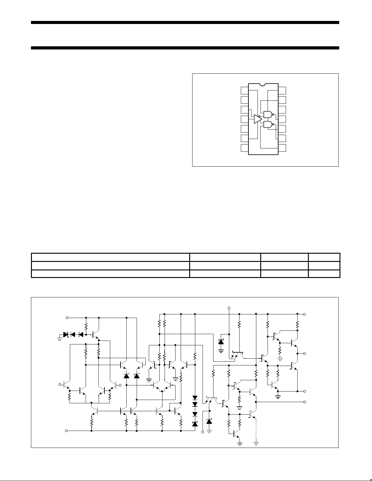
The NE527 is a high-speed analog voltage comparator which, for
the first time, mates state-of-the-art Schottky diode technology with
the conventional linear process. This allows simultaneous
fabrication of high speed TTL gates with a precision linear amplifier
on a single monolithic chip. The NE527 is similar in design to the
Philips Semiconductors NE529 voltage comparator except that it
incorporates an “Emitter-Follower” input stage for extremely low
input currents. This opens the door to a whole new range of
applications for analog voltage comparators.
FEATURES
•15ns propagation delay
•Complementary output gates
•TTL or ECL compatible outputs
•Wide common-mode and differential voltage range
•Typical gain of 5000
PIN CONFIGURATIONS
1
2
3
4
5
6
7 8
14
13
12
11
10
9
V1
+
NC
INPUT A
INPUT B
NC
V1
–
NC
V2
+
STROBE A
OUTPUT A
NC
GND
OUTPUT B
STROBE B
D, N Packages
TOP VIEW
APPLICATIONS
•A/D conversion
•ECL-to-TTL interface
•TTL-to-ECL interface
•Memory sensing
•Optical data coupling
ORDERING INFORMATION
DESCRIPTION TEMPERATURE RANGE ORDER CODE DWG #
14-Pin Plastic Dual In-Line Package (DIP) 0 to +70°C NE527N 0405B
14-Pin Small Outline (SO) Package 0 to +70°C NE527D 0175D
EQUIVALENT SCHEMATIC
V
1
20K
1.5K 1.5K
INPUT A
INPUT
B
200
V
1
300300 100 200
750
750
6.13K
1K 1K
STROBE B
20K
4K 1.5K
STROBE A
4K
250 500
4K
55
250
500
GND
OUTPUT B
OUTPUT A
4K
1.5K
V2
+
55
7.5K
–
7.5K
+
Page 2

Philips Semiconductors Linear Products Product specification
NE527Voltage comparator
August 31, 1994
316
ABSOLUTE MAXIMUM RATINGS
SYMBOL PARAMETER RATING UNIT
V1+ Positive supply voltage +15 V
V1- Negative supply voltage -15 V
V2+ Gate supply voltage +7 V
V
OUT
Output voltage +7 V
V
IN
Differential input voltage ±5 V
V
CM
Input common mode voltage ±6 V
P
D
Max power dissipation
1
25°C ambient (still air)
N package 1420 mW
D package 1040 mW
T
A
Operating temperature range 0 to +70 °C
T
STG
Storage temperature range -65 to +150 °C
T
SOLD
Lead soldering temperature (10sec max) +300 °C
NOTES:
1. Derate above 25°C, at the following rates:
N package 11.4mW/°C
D package 8.3mW/°C
BLOCK DIAGRAM
V
1
+
STROBE A
OUTPUT A
INPUT A
INPUT B
OUTPUT B
STROBE B
V
1
–
V
2
+
Page 3
Philips Semiconductors Linear Products Product specification
NE527Voltage comparator
August 31, 1994
317
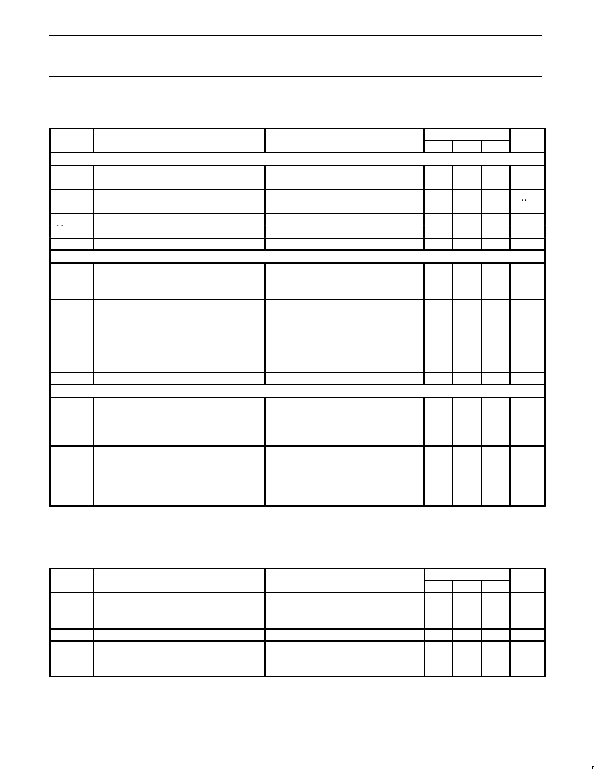
DC ELECTRICAL CHARACTERISTICS
V1+=10V, V1-=-10V, V2+=+5.0V, unless otherwise specified.
NE527
SYMBOL
PARAMETER
TEST CONDITIONS
Min Typ Max
UNIT
Input characteristics
Input offset voltage @ 25°C 6
V
OS
over temperature range 10
mV
Input bias current @ 25°C 2
I
BIAS
over temperature range 4
µA
Input offset current @ 25°C 0.75 µA
I
OS
over temperature range VIN=0V 1 µA
V
CM
Common-mode voltage range -5 +5 V
Gate characteristics
Output Voltage
“1” State V2+=4.75V, I
SOURCE
=-1mA 2.7 3.3 V
OUT
“0” State V2+=4.75V, I
SINK
=10mA 0.5 V
Strobe inputs
“0” Input current
1
V2+=5.25V, V
STROBE
=0.5V -2 mA
“1” Input current @ 25°C
1
V2+=5.25V, V
STROBE
=2.7V 100 µA
Over temperature range V2+=5.25V, V
STROBE
=2.7V 200 µA
“0” Input voltage V2+=4.75V 0.8 V
“1” Input voltage V2+=4.75V 2.0 V
I
SC
Short-circuit output current V2+=5.25V, V
OUT
=0V -18 -70 mA
Power supply requirements
Supply voltage
V1+ 5 10 V
V1- -6 -10 V
V2+ 4.75 5 5.25 V
Supply current V1+=10V, V1-=-10V
V2+=5.25V
I1+ Over temp. 5 mA
I1- Over temp. 10 mA
I2+ Over temp. 20 mA
NOTES:
1. See Logic Function Table.
AC ELECTRICAL CHARACTERISTICS
TA=25°C, unless otherwise specified. (See AC test circuit)
LIMITS
SYMBOL
PARAMETER
TEST CONDITIONS
Min Typ Max
UNIT
Transient response propagation delay time
t
PLH
Low-to-High VIN=±100mV step 16 26 ns
t
PHL
High-to-Low 14 24 ns
Delay between output A and B 2 5 ns
Strobe delay time
t
ON
Turn-on time 6 ns
t
OFF
Turn-off time 6 ns
V
OUT
Page 4
Philips Semiconductors Linear Products Product specification
NE527Voltage comparator
August 31, 1994
318
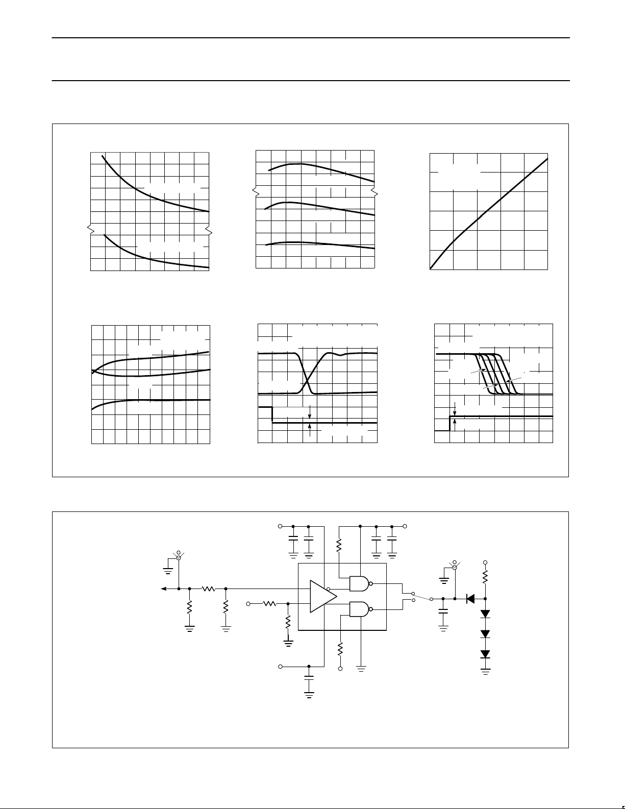
TYPICAL PERFORMANCE CHARACTERISTICS
OFFSET CURRENT
3.0
2.5
2.0
1.5
0
1.0
0.3
0.2
0.1
0
–50 –25 0 25 50 75 100 125
TEMPERATURE —
o
C
INOUR CURRENT — A
µ
I
2
+
V2 + = 5.0V
V1 – = 10V
V1 + = 10V
I
1
–
I
1
+
15
14
13
7
6
5
4
3
2
–50 –25 0 25 50 75 100
TEMPERATURE —
o
C
SUPPLY CURRENT — mA
V
2
+
=
5.0V
TA = 25
o
C
160
150
140
130
120
110
100
5 6 7 8 9 10
SUPPLY VOLTAGE (V
1
+
, V
1
–
) — VOLTS
POWER DISSIPATION — mW
TA = 25oC
V
2
+
= 5.0V
T
1
–
T
2
+
T
1
+
8
7
6
5
4
3
2
1
0
5 6 7 8 9 10
SUPPLY CURRENT — mA
SUPPLY VOLTAGE (V
1
+
, V
1
–
) — VOLTS
OUTPUT A
OUTPUT B
V
1
+
= 10V, V
1
–
= — 10V
V
2
+
= 5.0V
INPUT A
OVERDRIVE
5
4
3
2
1
0
+100
0
–100
0 5 10 15 20 25 30
TIME — ns
INPUT
VOLTAGE — V
OUTPUT
VOLTAGE — mV
V
1
+
= 10V, V
1
–
= — 10V
V
2
+
= 5.0V
OVERDRIVE
OVERDRIVE
INPUT B
OUTPUT A
5
4
3
2
1
0
+100
0
–100
0 5 10 15 20 25 30
TIME — ns
+
50mV
+
25mV
+
15mV
+
10mV
+
5mV
Input Currents vs Temperature Supply Currents vs Temperature
Power Dissipation
vs Supply Voltage
Supply Current
vs Supply Voltage
Output Propagation Delays
Response Time for
Various Input Overdrives
INPUT
VOLTAGE — V
OUTPUT
VOLTAGE — mV
BIAS CURRENT
INPUT PROBE
500Ω
INPUT
51Ω 51Ω
R1
+ 5
R2
+
.1
11K13
3
4
R3
6 8
1K
(V1 +)
+10
10µF
(V1 –)
–10
.1
+5
10
9
11
.1
14
(V2 +)
+5
10µF
+
OUTPUT
PROBE
+5
R
L
5K
CR1
CR2
CR3
CR4
C
L
NOTES:
CR1 — CR4 = IN914
R1 selected for 15.1 divider
R2, 3 selected for 100mV at Pin 4
Input
PRR = 1MHz
P
w
= 50ns
T
r
= Tf = 2ns
Amplitude = 3.00V
Output
R
L
= 390Ω
C
L
= 25pF (including
stray capacitance
RESPONSE TIME TEST CIRCUIT
Page 5
Philips Semiconductors Linear Products Product specification
NE527Voltage comparator
August 31, 1994
319
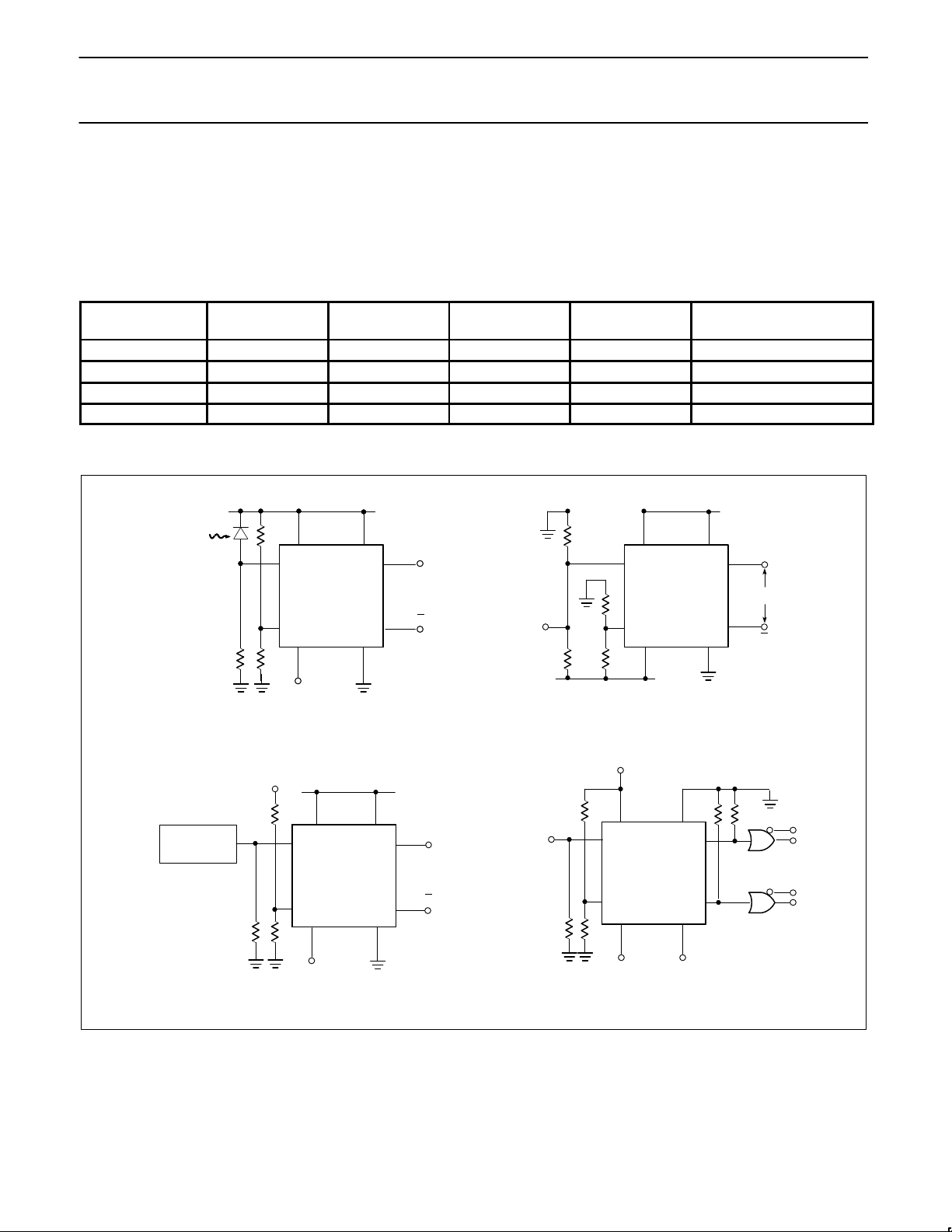
APPLICATIONS
One of the main features of the device is that supply voltages (V1+,
V
1
-) need not be balanced, as in the following diagrams. For proper
operation, however, negative supply (V
1
-) should always be at least
6V more than the ground terminal (Pin 6). Input common-mode
range should be limited to values of 2V less than the supply voltages
(V
1
+ and V1-) up to a maximum of ±5V as supply voltages are
increased. It is also important to note that Output A is in phase with
Input A and Output B is in phase with Input B.
LOGIC FUNCTION
V
ID
(A+, B–)
STROBE A STROBE B OUTPUT A OUTPUT B COMMENT
VID≤-V
OS
H X L H Read I
IHA
, I
ILB
-VOS<VID<V
OS
H H Undefined Undefined
VID≥V
OS
X H H L Read I
ILA
, I
IHB
X L L H H
TYPICAL APPLICATIONS
+ 5V
3
1 14 Q
Q
11
527N
9
10
6
4
R1R1
R2
R2
ECL
INPUT
TTL OUTPUTS
– 10V
λ
+ 5V
R2
3
1 14 Q
Q
11
529N
9
10
6
4
– 6V
R1
λ
R2
3
1 14 Q
Q
11
527N
9
10
6
4
– 6V
R1
Q
Q
3
1 14
11
529N
9
10
6
4
3
1 14
11
527N
9
10
6
4
1103
MOS RAM
V
REF
+ 5V
100Ω 100Ω
– 6V
3
1 14
11
529N
9
10
6
4
3
1 14
11
527N
9
10
6
4
+ 5V
TTL INPUT
3R
1
R
1
R
1
– 10V – 5.2V
2K 2K
Photodiode Detector ECL–to–TTL Interface
MOS Memory Sense AMP TTL–to–ECL Interface
 Loading...