

Page 1

Philips Semiconductors Product specification
NE5210Transimpedance amplifier (280MHz)
1
1995 Apr 26 853-1654 15170
DESCRIPTION
The NE5210 is a 7kΩ transimpedance wide band, low noise
amplifier with differential outputs, particularly suitable for signal
recovery in fiber-optic receivers. The part is ideally suited for many
other RF applications as a general purpose gain block.
FEATURES
•Low noise: 3.5pA/√Hz
•Single 5V supply
•Large bandwidth: 280MHz
•Differential outputs
•Low input/output impedances
•High power supply rejection ratio
•High overload threshold current
•Wide dynamic range
•7kΩ differential transresistance
APPLICATIONS
•Fiber-optic receivers, analog and digital
•Current-to-voltage converters
PIN CONFIGURATION
1
2
3
4
5
6
7 8
14
13
12
11
10
9
GND
2
GND
2
NC
I
IN
NC
V
CC1
V
CC2
GND
1
GND
1
GND
1
GND
1
GND
2
OUT (–)
OUT (+)
D Package
TOP VIEW
SD00318
•Wideband gain block
•Medical and scientific instrumentation
•Sensor preamplifiers
•Single-ended to differential conversion
•Low noise RF amplifiers
•RF signal processing
ORDERING INFORMATION
DESCRIPTION TEMPERATURE RANGE ORDER CODE DWG #
14-Pin Plastic Small Outline (SO) Package 0 to +70°C NE5210D SOT108-1
ABSOLUTE MAXIMUM RATINGS
SYMBOL PARAMETER RATING UNIT
V
CC
Power supply 6 V
T
A
Operating ambient temperature range 0 to +70 °C
T
J
Operating junction temperature range -55 to +150 °C
T
STG
Storage temperature range -65 to +150 °C
P
DMAX
Power dissipation, TA=25°C (still air)
1
1.0 W
I
INMAX
Maximum input current
2
5 mA
NOTES:
1. Maximum dissipation is determined by the operating ambient temperature and the thermal resistance: θ
JA
=125°C/W.
2. The use of a pull-up resistor to VCC for the PIN diode, is recommended.
RECOMMENDED OPERATING CONDITIONS
SYMBOL PARAMETER RATING UNIT
V
CC
Supply voltage 4.5 to 5.5 V
T
A
Ambient temperature range 0 to +70 °C
T
J
Junction temperature range 0 to +90 °C
Page 2

Philips Semiconductors Product specification
NE5210Transimpedance amplifier (280MHz)
1995 Apr 26
2
DC ELECTRICAL CHARACTERISTICS
Min and Max limits apply over operating temperature range at VCC=5V, unless otherwise specified. Typical data applies at VCC=5V and
T
A
=25°C.
LIMITS
SYMBOL
PARAMETER
TEST CONDITIONS
Min Typ Max
UNIT
V
IN
Input bias voltage 0.6 0.8 0.95 V
V
O
±
Output bias voltage 2.8 3.3 3.7 V
V
OS
Output offset voltage 0 80 mV
I
CC
Supply current 21 26 32 mA
I
OMAX
Output sink/source current
1
3 4 mA
I
IN
Input current (2% linearity) Test Circuit 8, Procedure 2 ±120 ±160 µA
I
INMAX
Maximum input current
overload threshold
Test Circuit 8, Procedure 4 ±160 ±240 µA
NOTES:
1. Test condition: output quiescent voltage variation is less than 100mV for 3mA load current.
AC ELECTRICAL CHARACTERISTICS
Typical data and Min/Max limits apply at VCC=5V and TA=25°C.
LIMITS
SYMBOL
PARAMETER
TEST CONDITIONS
Min Typ Max
UNIT
R
T
Transresistance
(differential output)
DC tested, RL=∞
Test Circuit 8, Procedure 1
4.9 7 10 kΩ
R
O
Output resistance
(differential output)
DC tested 16 30 42 Ω
R
T
Transresistance
(single-ended output)
DC tested, RL=∞ 2.45 3.5 5 kΩ
R
O
Output resistance
(single-ended output)
DC tested 8 15 21 Ω
f
3dB
Bandwidth (-3dB) Test Circuit 1, TA=25°C 200 280 MHz
R
IN
Input resistance 60 Ω
C
IN
Input capacitance 7.5 pF
∆R/∆V
Transresistance power
supply sensitivity
VCC=5±0.5V 9.6 20 %/V
∆R/∆T
Transresistance ambient
temperature sensitivity
∆TA=T
A MAX-TA MIN
0.05 0.1 %/°C
I
N
RMS noise current spectral density
(referred to input)
f=10MHz, TA=25°C
Test Circuit 2
3.5 6 pA/√Hz
TA=25°C
Test Circuit 2
Integrated RMS noise current over
the bandwidth (referred to input)
∆f=100MHz 37
the bandwidth (referred to input)
C
S
=0
1
∆f=200MHz 56
I
T
∆f=300MHz 71
nA
∆f=100MHz 40
∆f=200MHz 66
S
=1pF
∆f=300MHz 89
PSRR
Power supply rejection ratio
2
(V
CC1=VCC2
)
DC tested, ∆VCC=0.1V
Equivalent AC test circuit 3
20 36 dB
PSRR
Power supply rejection ratio
2
(V
CC1
)
DC tested, ∆VCC=0.1V
Equivalent AC test circuit 4
20 36 dB
PSRR
Power supply rejection ratio
2
(V
CC2
)
DC tested, ∆VCC=0.1V
Equivalent AC test circuit 5
65 dB
PSRR
Power supply rejection ratio2 (ECL
configuration)
f=0.1MHz, Test Circuit 6 23 dB
CS=1pF
Page 3
Philips Semiconductors Product specification
NE5210Transimpedance amplifier (280MHz)
1995 Apr 26
3
AC ELECTRICAL CHARACTERISTICS (Continued)
LIMITS
SYMBOL
PARAMETER
TEST CONDITIONS
Min Typ Max
UNIT
V
OMAX
Maximum output voltage swing differential
RL=∞
Test Circuit 8, Procedure 3
2.4 3.2 V
P-P
V
INMAX
Maximum input amplitude for
output duty cycle of 50±5%
3
Test Circuit 7 650 mV
P-P
t
R
Rise time for 50 mV
P-P
output signal
4
Test Circuit 7 0.8 1.2 ns
NOTES:
1. Package parasitic capacitance amounts to about 0.2pF
2. PSRR is output referenced and is circuit board layout dependent at higher frequencies. For best performance use RF filter in V
CC
line.
3. Guaranteed by linearity and overload tests.
4. t
R
defined as 20-80% rise time. It is guaranteed by a -3dB bandwidth test.
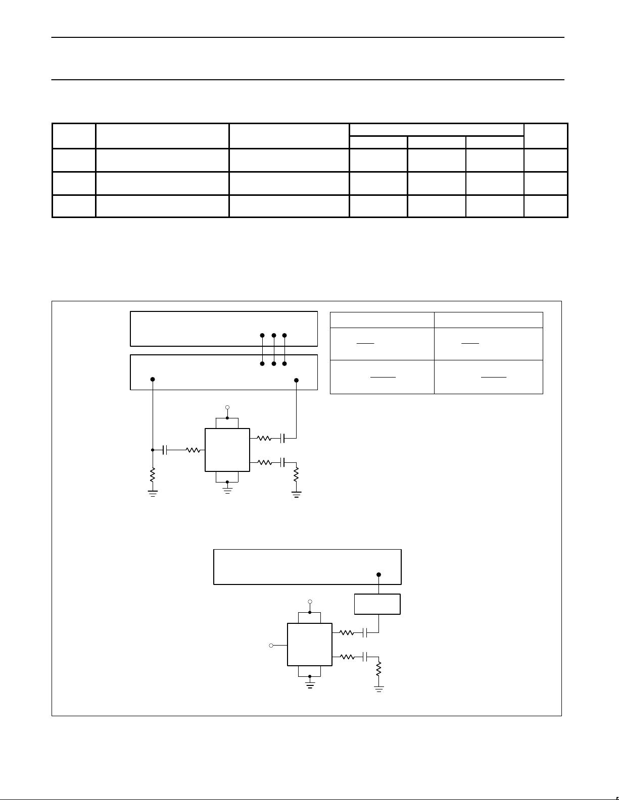
TEST CIRCUITS
Test Circuit 2
Test Circuit 1
R
T
V
OUT
V
IN
R 2 S21 R R
T
V
OUT
V
IN
R 4 S21 R
SINGLE-ENDED DIFFERENTIAL
RO Z
O
1 S22
1 S22
33 RO 2Z
O
1 S22
1 S22
66
NETWORK ANALYZER
S-PARAMETER TEST SET
PORT 1
PORT 2
5V
33
IN DUT
OUT
OUT
50
33
GND
1
GND
2
V
CC1VCC2
ZO = 50
0.1µF
R
L
= 50
R = 1k
0.1µF
0.1µF
SPECTRUM ANALYZER
5V
33
IN DUT
OUT
OUT
33
GND
1
GND
2
V
CC1VCC2
0.1µF
RL = 50
0.1µF
AV = 60DB
NC
Z
O
= 50
Z
O
= 50
SD00319
Page 4

Philips Semiconductors Product specification
NE5210Transimpedance amplifier (280MHz)
1995 Apr 26
4
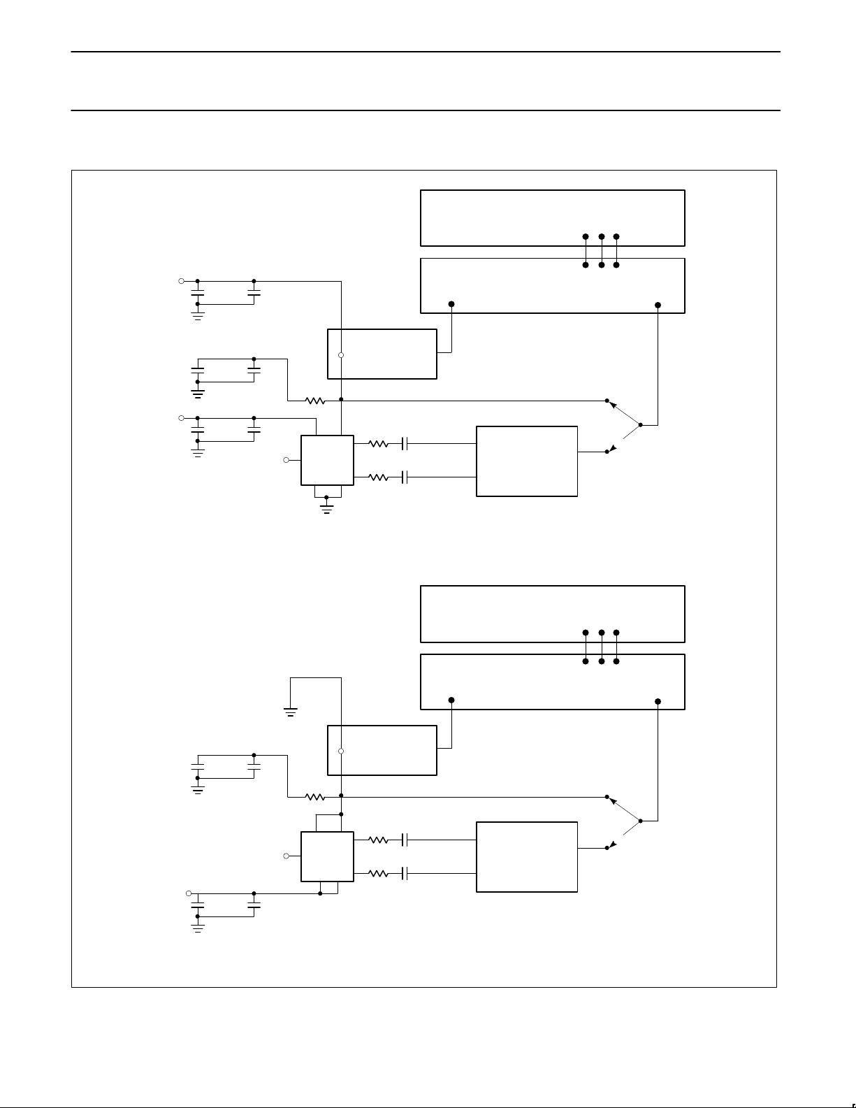
TEST CIRCUITS (Continued)
Test Circuit 4
Test Circuit 3
NETWORK ANALYZER
S-PARAMETER TEST SET
PORT 1 PORT 2
V
CC2
V
CC1
GND
1
GND
2
IN
CURRENT PROBE
1mV/mA
CAL
TEST
TRANSFORMER
NH0300HB
100
33
33
16
5V
OUT
OUT
BAL.
0.1µF
0.1µF
10µF
0.1µF
0.1µF
50
UNBAL.
NETWORK ANALYZER
S-PARAMETER TEST SET
PORT 1 PORT 2
CURRENT PROBE
1mV/mA
CAL
TEST
TRANSFORMER
NH0300HB
100
33
33
16
5V
OUT
OUT
BAL.
50
UNBAL.
V
CC1
V
CC2
IN
0.1µF
0.1µF
10µF
0.1µF
0.1µF
0.1µF
10µF
5V
10µF
10µF
GND
1
GND
2
SD00320
Page 5
Philips Semiconductors Product specification
NE5210Transimpedance amplifier (280MHz)
1995 Apr 26
5
TEST CIRCUITS (Continued)
NETWORK ANALYZER
S-PARAMETER TEST SET
PORT 1 PORT 2
CURRENT PROBE
1mV/mA
CAL
TEST
TRANSFORMER
NH0300HB
100
33
33
16
5V
OUT
OUT
BAL.
50
UNBAL.
V
CC2
V
CC1
IN
0.1µF
0.1µF
10µF
0.1µF
0.1µF
0.1µF
10µF
5V
Test Circuit 6
Test Circuit 5
NETWORK ANALYZER
S-PARAMETER TEST SET
PORT 1 PORT 2
CURRENT PROBE
1mV/mA
CAL
TEST
TRANSFORMER
NH0300HB
100
33
33
16
OUT
OUT
BAL.
50
UNBAL.
GND
2
GND
1
V
CC1
V
CC2
IN
0.1µF
0.1µF
0.1µF
10µF
GND
0.1µF
10µF
5.2V
10µF
GND
2
GND
1
SD00321
Page 6
Philips Semiconductors Product specification
NE5210Transimpedance amplifier (280MHz)
1995 Apr 26
6
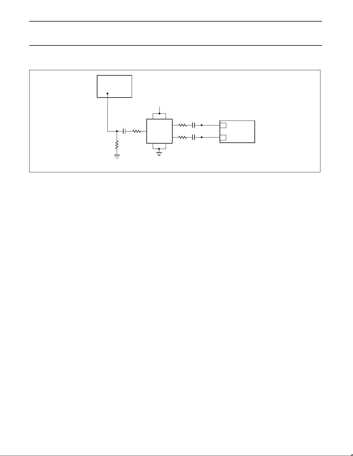
TEST CIRCUITS (Continued)
Test Circuit 7
OSCILLOSCOPE
33
33
1k
OUT
OUT
GND
2
GND
1
V
CC1VCC2
IN
0.1µF
0.1µF
PULSE GEN.
Measurement done using
differential wave forms
0.1µF
50
Z
O
= 50Ω
A
B
Z
O
= 50Ω
DUT
SD00322
Page 7
Philips Semiconductors Product specification
NE5210Transimpedance amplifier (280MHz)
1995 Apr 26
7
TEST CIRCUITS (Continued)
GND
2
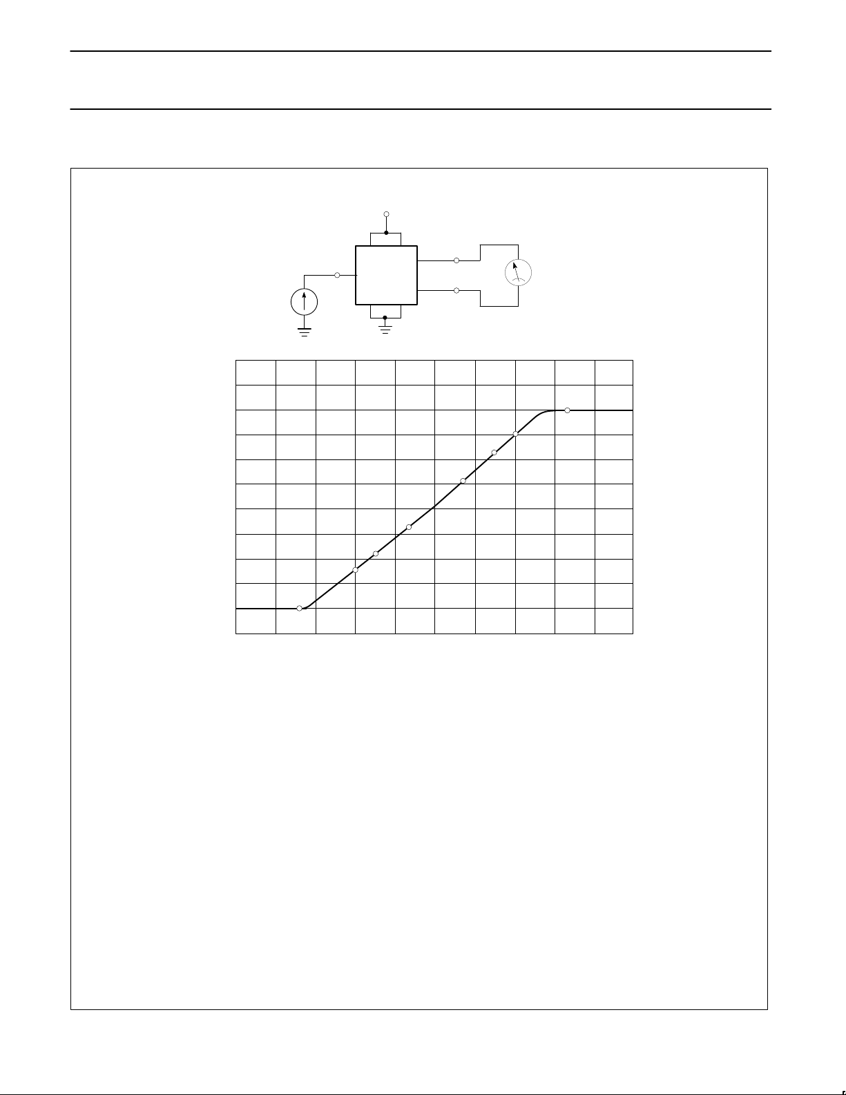
Test Circuit 8
OUT +
OUT –
GND
1
IN
DUT
IIN (µA)
5V
V
OUT
(V)
+
–
Typical Differential Output Voltage
vs Current Input
2.00
1.60
1.20
0.80
0.40
0.00
–0.40
–0.80
–1.20
–1.60
–2.00
–400 –320 –240 –160 –80 0 80 160 240 320 400
DIFFERENTIAL OUTPUT VOLTAGE (V)
CURRENT INPUT (µA)
NE5210 TEST CONDITIONS
Procedure 1
R
T
measured at 60µA
R
T
= (VO1 – VO2)/(+60µA – (–60µA))
Where: V
O1
Measured at IIN = +60µA
V
O2
Measured at IIN = –60µA
Procedure 2
Linearity = 1 – ABS((V
OA
– VOB) / (VO3 – VO4))
Where: VO3 Measured at IIN = +120µA
V
O4
Measured at IIN = –120µA
VOA RT ( 120A) V
OB
VOB RT ( 120A) V
OB
Procedure 3
V
OMAX
= VO7 – V
O8
Where: VO7 Measured at IIN = +260µA
V
O8
Measured at IIN = –260µA
Procedure 4
I
IN
Test Pass Conditions:
V
O7
– VO5 > 20mV and V06 – VO5 > 20mV
Where: V
O5
Measured at IIN = +160µA
V
O6
Measured at IIN = –160µA
VO7 Measured at IIN = +260µA
V
O8
Measured at IIN = –260µA
SD00323
Page 8

Philips Semiconductors Product specification
NE5210Transimpedance amplifier (280MHz)
1995 Apr 26
8
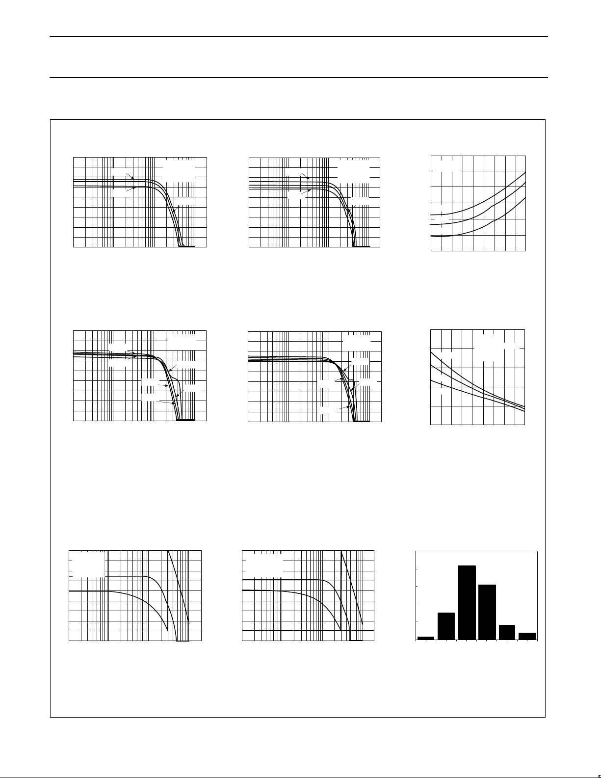
TYPICAL PERFORMANCE CHARACTERISTICS
DIFFERENTIAL OUTPUT VOLTAGE (V) DIFFERENTIAL OUTPUT VOLTAGE (V)
OUTPUT VOLTAGE (V)
OUTPUT BIAS VOLTAGE (V)
AMBIENT TEMPERATURE (°C)
AMBIENT TEMPERATURE (°C)
NE5210 Supply Current
vs Temperature
NE5210 Output Bias Voltage
vs Temperature
Output Voltage
vs Input Current
NE5210 Input Bias Voltage
vs Temperature
NE5210 Output Bias Voltage
vs Temperature
Differential Output Voltage
vs Input Current
NE5210 Output Offset Voltage
vs Temperature
NE5210 Differential Output Swing
vs Temperature
Differential Output Voltage
vs Input Current
AMBIENT TEMPERATURE (°C)
–10 10 20 30 40 50 60 70 80
32
30
28
26
24
22
20
18
0
TOTAL SUPPLY CURRENT (mA)
(I + I )
CC1
CC2
3.50
3.46
3.42
3.38
3.34
3.30
–10 10 20 30 40 50 60 70 800
OUTPUT BIAS VOLTAGE (V)
VCC = 5.0V
PIN 14
PIN 12
–10 10 20 30 40 50 60 70 80
900
0
INPUT BIAS VOLTAGE (mV)
850
800
750
700
5.5V
5.0V
4.5V
–10 10 20 30 40 50 60 70 80
20
0
OUTPUT OFFSET VOLTAGE (mV)
0
–20
–40
–60
5.5V
5.0V
4.5V
AMBIENT TEMPERATURE (°C)
–80
VOS = V
OUT12
– V
OUT14
–10 10 20 30 40 50 60 70 800
AMBIENT TEMPERATURE (°C)
4.1
3.9
3.7
3.5
3.3
3.1
2.9
2.7
PIN 14
5.5V
5.0V
4.5V
DIFFERENTIAL OUTPUT SWING (V)
–10 10 20 30 40 50 60 70 800
4.0
3.8
3.6
3.4
3.2
3.0
2.8
2.6
AMBIENT TEMPERATURE (°C)
5.5V
5.0V
4.5V
2.4
2.2
DC TESTED
RL = ∞
4.5
3.0
2.5
–300.0 0 +300.0
INPUT CURRENT (µA)
+25°C
+125°C
+85°C
–55°C
+125°C
+85°C
2.0
0
–2.0
–300.0 0 +300.0
INPUT CURRENT (µA)
5.5V
5.0V
4.5V
5.5V
5.0V
4.5V
2.0
0
–2.0
–300.0 0 +300.0
INPUT CURRENT (µA)
+125°C
+85°C
+25°C
–55°C
SD00324
Page 9
Philips Semiconductors Product specification
NE5210Transimpedance amplifier (280MHz)
1995 Apr 26
9
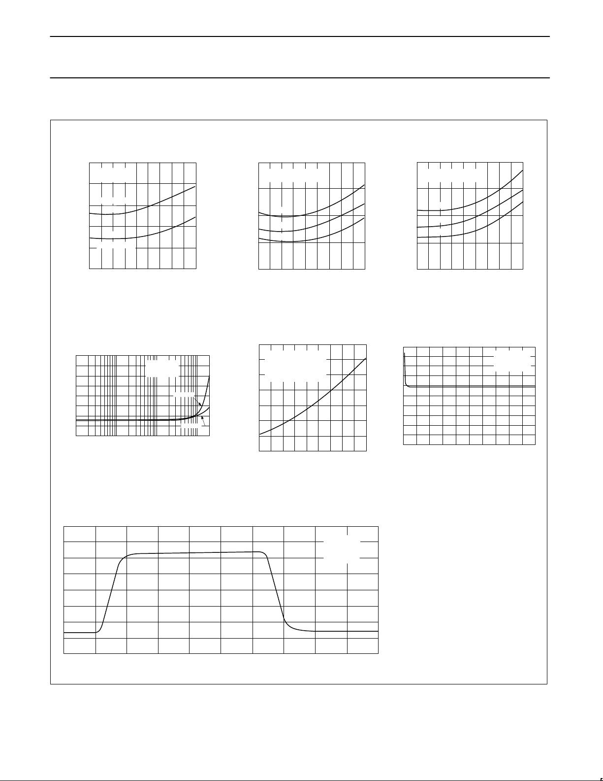
TYPICAL PERFORMANCE CHARACTERISTICS (Continued)
8
7
6
5
4
3
2
1
0
–1
GAIN (dB)
POPULATION (%)
Gain vs Frequency Gain vs Frequency
NE5210 Differential Transresistance
vs Temperature
Gain vs Frequency Gain vs Frequency NE5210 Bandwidth vs Temperature
Gain and Phase Shift
vs Frequency
NE5210 Typical
Bandwidth Distribution
(70 Parts from 4 Wafer Lots)
Gain and Phase Shift
vs Frequency
50
40
30
20
10
0
223 255 287 319 351 383
FREQUENCY (MHz)
PIN 12
SINGLE-ENDED
RL = 50Ω
V
CC
= 5.0V
TA = 25°C
AMBIENT TEMPERATURE (°C)
8.6
–10 10 20 30 40 50 60 70 800
DIFFERENTIAL TRANSRESISTANCE (k )
RL = ∞
8.4
8.2
8.0
7.8
7.6
7.4
Ω
5.5V
5.0V
4.5V
450
–10 10 20 30 40 50 60 70 800
BANDWIDTH (MHz)
AMBIENT TEMPERATURE (°C)
400
350
300
250
200
5.5V
5.0V
4.5V
PIN 12
PIN 12
VCC = 5V
TA = 25°C
8
7
6
5
4
3
2
1
0
–1
1 10 100 1000
FREQUENCY (MHz)
GAIN (dB)
180
90
0
–90
–180
PHASE ( )
o
1 10 100 1000
FREQUENCY (MHz)
PIN 12
VCC = 5V
8
7
6
5
4
3
2
1
0
–1
GAIN (dB)
–55°C
+125°C
+85°C
25°C
+125°C
–55°C
1 10 100 1000
FREQUENCY (MHz)
PIN 12
VCC = 5V
RL = 50Ω
5.0V
5.5V
4.5V
8
7
6
5
4
3
2
1
0
–1
GAIN (dB)
1 10 100 1000
FREQUENCY (MHz)
PIN 12
VCC = 5V
R
L
= 50Ω
5.0V
5.5V
4.5V
1 10 100 1000
FREQUENCY (MHz)
PIN 14
8
7
6
5
4
3
2
1
0
–1
GAIN (dB)
VCC = 5V
–55°C
+125°C
25°C
85°C
PIN 14
8
7
6
5
4
3
2
1
0
–1
1 10 100 1000
FREQUENCY (MHz)
GAIN (dB)
360
270
180
90
0
PHASE ( )
o
VCC = 5V
T
A
= 25°C
RL = Ω
SINGLE-ENDED
SD00325
Page 10
Philips Semiconductors Product specification
NE5210Transimpedance amplifier (280MHz)
1995 Apr 26
10
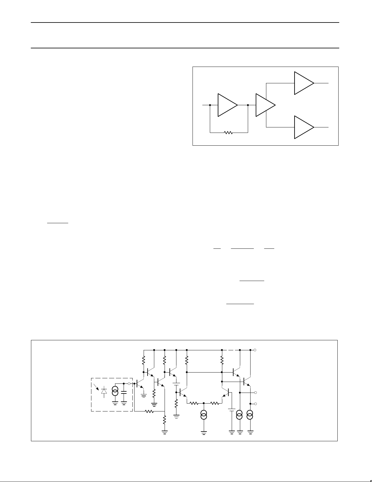
TYPICAL PERFORMANCE CHARACTERISTICS (Continued)
FREQUENCY (MHz)
NE5210 Output Resistance
vs Temperature
NE5210 Output Resistance
vs Temperature
NE5210 Output Resistance
vs Temperature
Output Resistance
vs Frequency
NE5210 Power Supply Rejection Ratio
vs Temperature
Group Delay
Output Step Response
0 2 4 6 8 10 12 14 16 18 20
(ns)
VCC = 5V
TA = 25°C
20mV/Div
VCC = 5V
TA = 25°C
10
8
6
4
2
0
0.1 20 40 60 80 100 120 140 160 180 200
DELAY (ns)
40
39
38
37
36
35
34
33
–10 0 10 20 30 40 50 60 70 80
POWER SUPPLY REJECTION RATIO (dB)
AMBIENT TEMPERATURE (°C)
V
CC1
= V
CC2
= 5.0V
∆VCC = ±0.1V
DC TESTED
OUTPUT REFERRED
17
16
15
14
13
–10 0 10 20 30 40 50 60 70 80
AMBIENT TEMPERATURE (°C)
OUTPUT RESISTANCE ( )
Ω
PIN 14
OUTPUT REFERRED
4.5V
5.0V
5.5V
16
15
14
13
12
–10 0 10 20 30 40 50 60 70 80
OUTPUT RESISTANCE ( )
Ω
PIN 12
OUTPUT REFERRED
4.5V
5.0V
5.5V
AMBIENT TEMPERATURE (°C)
17
16
15
14
13
–10 0 10 20 30 40 50 60 70 80
OUTPUT RESISTANCE ( )
Ω
VCC = 5.0V
DC TESTED
5.0V
AMBIENT TEMPERATURE (°C)
12
PIN 14 R
OUT
PIN 12 R
OUT
5.0V
80
70
60
50
40
30
20
10
0
OUTPUT RESISTANCE ( )
Ω
FREQUENCY (MHz)
0.1 1 10 100 200
PIN 12
PIN 14
VCC = 5.0V
T
A
= 25°C
SD00326
Page 11
Philips Semiconductors Product specification
NE5210Transimpedance amplifier (280MHz)
1995 Apr 26
11
THEORY OF OPERATION
Transimpedance amplifiers have been widely used as the
preamplifier in fiber-optic receivers. The NE5210 is a wide
bandwidth (typically 280MHz) transimpedance amplifier designed
primarily for input currents requiring a large dynamic range, such as
those produced by a laser diode. The maximum input current before
output stage clipping occurs at typically 240µA. The NE5210 is a
bipolar transimpedance amplifier which is current driven at the input
and generates a differential voltage signal at the outputs. The
forward transfer function is therefore a ratio of the differential output
voltage to a given input current with the dimensions of ohms. The
main feature of this amplifier is a wideband, low-noise input stage
which is desensitized to photodiode capacitance variations. When
connected to a photodiode of a few picoFarads, the frequency
response will not be degraded significantly. Except for the input
stage, the entire signal path is differential to provide improved
power-supply rejection and ease of interface to ECL type circuitry. A
block diagram of the circuit is shown in Figure 1. The input stage
(A1) employs shunt-series feedback to stabilize the current gain of
the amplifier. The transresistance of the amplifier from the current
source to the emitter of Q
3
is approximately the value of the
feedback resistor, R
F
=3.6kΩ. The gain from the second stage (A2)
and emitter followers (A3 and A4) is about two. Therefore, the
differential transresistance of the entire amplifier , R
T
is
R
T
V
OUT
(diff)
I
IN
2RF 2(3.6K) 7.2kW
The single-ended transresistance of the amplifier is typically 3.6kΩ.
The simplified schematic in Figure 2 shows how an input current is
converted to a differential output voltage. The amplifier has a single
input for current which is referenced to Ground 1. An input current
from a laser diode, for example, will be converted into a voltage by
the feedback resistor R
F
. The transistor Q1 provides most of the
open loop gain of the circuit, A
VOL
≈70. The emitter follower Q
2
minimizes loading on Q1. The transistor Q4, resistor R7, and V
B1
provide level shifting and interface with the Q15 – Q16 differential
pair of the second stage which is biased with an internal reference,
V
B2
. The differential outputs are derived from emitter followers Q
11
–
Q
12
which are biased by constant current sources. The collectors of
Q
11
– Q12 are bonded to an external pin, V
CC2
, in order to reduce
the feedback to the input stage. The output impedance is about 17Ω
single-ended. For ease of performance evaluation, a 33Ω resistor is
used in series with each output to match to a 50Ω test system.
INPUT
OUTPUT +
OUTPUT –
A1 A2
A3
A4
R
F
SD00327
Figure 1. NE5210 – Block Diagram
BANDWIDTH CALCULATIONS
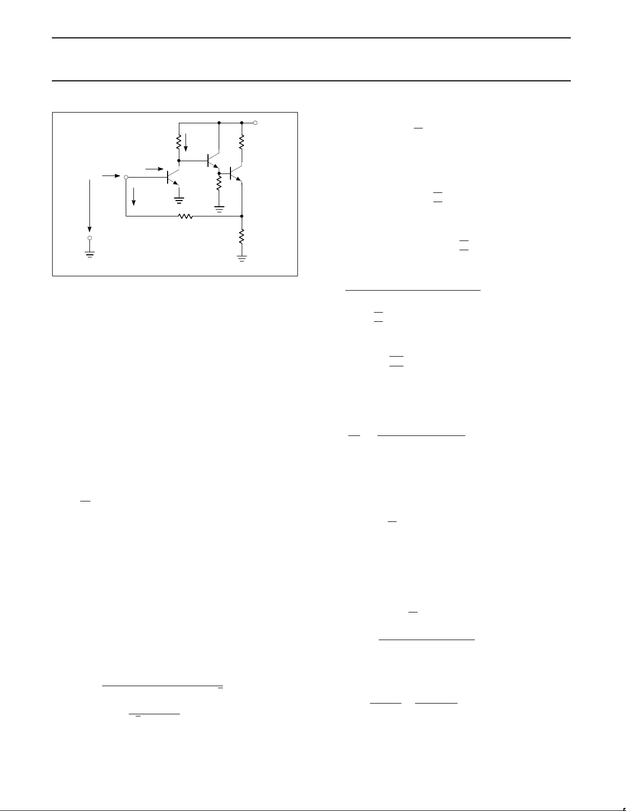
The input stage, shown in Figure 3, employs shunt-series feedback
to stabilize the current gain of the amplifier. A simplified analysis can
determine the performance of the amplifier. The equivalent input
capacitance, C
IN
, in
parallel with the source, I
S
, is approximately 7.5pF, assuming that
C
S
=0 where CS is the external source capacitance.
Since the input is driven by a current source the input must have a
low input resistance. The input resistance, R
IN
, is the ratio of the
incremental input voltage, V
IN
, to the corresponding input current, I
IN
and can be calculated as:
R
IN
V
IN
I
IN
R
F
1 A
VOL
3.6K
71
51W
More exact calculations would yield a higher value of 60Ω.
Thus C
IN
and RIN will form the dominant pole of the entire amplifier;
f
3dB
1
2p R
INCIN
Assuming typical values for RF = 3.6kΩ, RIN = 60Ω, CIN = 7.5pF
f
3dB
1
2p 7.5pF 60
354MHz
INPUT
OUT–
OUT+
PHOTODIODE
VB2
+
+
R
1
R
3
R
12
R
13
R
5
R
4
R
7
R
14
R
15
Q
1
Q
3
Q
2
Q
4
Q
15
Q
16
Q
11
Q
12
GND
2
GND
1
V
CC2
V
CC1
R
2
SD00328
Figure 2. Transimpedance Amplifier
Page 12
Philips Semiconductors Product specification
NE5210Transimpedance amplifier (280MHz)
1995 Apr 26
12
V
CC
V
EQ3
V
IN
I
IN
INPUT
I
F
I
B
Q1
Q2
Q3
R2
R3
R4
R
F
R1
I
C1
SD00329
Figure 3. Shunt-Series Input Stage
The operating point of Q1, Figure 2, has been optimized for the
lowest current noise without introducing a second dominant pole in
the pass-band. All poles associated with subsequent stages have
been kept at sufficiently high enough frequencies to yield an overall
single pole response. Although wider bandwidths have been
achieved by using a cascode input stage configuration, the present
solution has the advantage of a very uniform, highly desensitized
frequency response because the Miller effect dominates over the
external photodiode and stray capacitances. For example, assuming
a source capacitance of 1pF, input stage voltage gain of 70, R
IN
=
60Ω then the total input capacitance, C
IN
= (1+7.5) pF which will
lead to only a 12% bandwidth reduction.
NOISE
Most of the currently installed fiber-optic systems use non-coherent
transmission and detect incident optical power. Therefore, receiver
noise performance becomes very important. The input stage
achieves a low input referred noise current (spectral density) of
3.5pA/√Hz
. The transresistance configuration assures that the
external high value bias resistors often required for photodiode
biasing will not contribute to the total noise system noise. The
equivalent input
RMS
noise current is strongly determined by the
quiescent current of Q
1
, the feedback resistor RF, and the
bandwidth; however, it is not dependent upon the internal
Miller-capacitance. The measured wideband noise was 66nA
RMS
in
a 200MHz bandwidth.
DYNAMIC RANGE CALCULATIONS
The electrical dynamic range can be defined as the ratio of
maximum input current to the peak noise current:
Electrical dynamic range, D
E
, in a 200MHz bandwidth assuming
I
INMAX
= 240µA and a wideband noise of IEQ=66nA
RMS
for an
external source capacitance of C
S
= 1pF.
D
E
+ 20log
(Max. input current) (PK)
(Peak noise current) (RMS)@ 2
Ǹ
+ 20log
(240 @ 10
*6
)
( 2
Ǹ
66 10*9)
+ 68dB
In order to calculate the optical dynamic range the incident optical
power must be considered.
For a given wavelength λ; (meters)
Energy of one Photon =
hc
l
watt sec (Joule)
Where h=Planck’s Constant = 6.6 × 10
-34
Joule sec.
c = speed of light = 3 × 10
8
m/sec
c / λ = optical frequency (Hz)
No. of incident photons/sec= where P=optical incident power
No. of incident photons/sec =
P
hs
l
where P = optical incident power
No. of generated electrons/sec =
h @
P
hs
l
where η = quantum efficiency
+
no. of generated electron hole paris
no. of incident photons
N I + h @
P
hs
l
@ e Amps (Coulombsń sec.)
where e = electron charge = 1.6 × 10
-19
Coulombs
Responsivity R =
h @e
hs
l
Amp/watt
I + P @ R
Assuming a data rate of 400 Mbaud (Bandwidth, B=200MHz), the
noise parameter Z may be calculated as:
1
Z +
I
EQ
qB
+
66 @ 10
*9
(1.6@ 10
*19
)(200 @ 106)
+ 2063
where Z is the ratio of
RMS
noise output to the peak response to a
single hole-electron pair. Assuming 100% photodetector quantum
efficiency, half mark/half space digital transmission, 850nm
lightwave and using Gaussian approximation, the minimum required
optical power to achieve 10
-9
BER is:
P
avMIN
+ 12
hc
l
B Z + 12 2.3@ 10
*19
200@ 1062063
+ 1139nW + * 29.4dBm
where h is Planck’s Constant, c is the speed of light, λ is the
wavelength. The minimum input current to the NE5210, at this input
power is:
I
avMIN
+ qP
avMIN
l
hc
+
1139@ 10
*9
@ 1.6 @ 10
*19
2.3@ 10
*19
= 792nA
Choosing the maximum peak overload current of I
avMAX
=240µA, the
maximum mean optical power is:
P
avMAX
+
hcI
avMAX
l q
+
2.3@ 10
*19
1.6@ 10
*19
240 @ 10
*6
Thus the optical dynamic range, DO is:
D
O
= P
avMAX
- P
avMIN
= -4.6 -(-29.4) = 24.8dB.
Page 13
Philips Semiconductors Product specification
NE5210Transimpedance amplifier (280MHz)
1995 Apr 26
13
This represents the maximum limit attainable with the NE5210
operating at 200MHz bandwidth, with a half mark/half space digital
transmission at 850nm wavelength.
APPLICATION INFORMATION
Package parasitics, particularly ground lead inductances and
parasitic capacitances, can significantly degrade the frequency
response. Since the NE5210 has differential outputs which can feed
back signals to the input by parasitic package or board layout
capacitances, both peaking and attenuating type frequency
response shaping is possible. Constructing the board layout so that
Ground 1 and Ground 2 have very low impedance paths has
produced the best results. This was accomplished by adding a
ground-plane stripe underneath the device connecting Ground 1,
Pins 8–11, and Ground 2, Pins 1 and 2 on opposite ends of the
SO14 package. This ground-plane stripe also provides isolation
between the output return currents flowing to either V
CC2
or Ground
2 and the input photodiode currents to flowing to Ground 1. Without
this ground-plane stripe and with large lead inductances on the
board, the part may be unstable and oscillate near 800MHz. The
easiest way to realize that the part is not functioning normally is to
measure the DC voltages at the outputs. If they are not close to their
quiescent values of 3.3V (for a 5V supply), then the circuit may be
oscillating. Input pin layout necessitates that the photodiode be
physically very close to the input and Ground 1. Connecting Pins 3
and 5 to Ground 1 will tend to shield the input but it will also tend to
increase the capacitance on the input and slightly reduce the
bandwidth.
As with any high-frequency device, some precautions must be
observed in order to enjoy reliable performance. The first of these is
the use of a well-regulated power supply. The supply must be
capable of providing varying amounts of current without significantly
changing the voltage level. Proper supply bypassing requires that a
good quality 0.1µF high-frequency capacitor be inserted between
V
CC1
and V
CC2
, preferably a chip capacitor, as close to the package
pins as possible. Also, the parallel combination of 0.1µF capacitors
with 10µF tantalum capacitors from each supply, V
CC1
and V
CC2
, to
the ground plane should provide adequate decoupling. Some
applications may require an RF choke in series with the power
supply line. Separate analog and digital ground leads must be
maintained and printed circuit board ground plane should be
employed whenever possible.
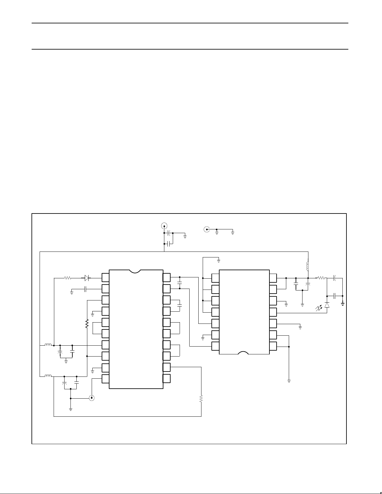
Figure 4 depicts a 50Mb/s TTL fiber-optic receiver using the BPF31,
850nm LED, the NE5210 and the NE5214 post amplifier.
1
2
3
4
5
6
7
8
9
10 11
12
13
14
15
16
17
18
19
20
1
2
3
4
5
6
78
9
10
11
12
13
14
LED
C
PKDET
THRESH
GND
A
FLAG
JAM
V
CCD
V
CCA
GND
D
TTL
OUT
IN
1B
IN
1A
C
AZP
C
AZN
OUT
1B
IN
8B
OUT
1A
IN
8A
R
HYST
R
PKDET
NE5214
GND
GND
GND
OUT
GND
GND
OUT
V
CC
V
CC
NC
I
IN
NC
GND
GND
NE5210
R2
220
D1
LED
C9
100pF
100pF
C7
.01µF
47µF
C1
C2
GND
+V
CC
0.1µF
R4
4k
R3
47k
V
OUT
(TTL)
L3
10µH
L2
10µH
C11
C10
.01µF
.01µF
C13
C12
10µF
10
µF
C8
L1
10µH
BPF31
OPTICAL
INPUT
R1
100
C5
1.0µF
C6
.01µF
.01µF
C4
10µF
C3
NOTE:
The NE5210/NE5217 combination can operate at data rates in excess of 100Mb/s NRZ
The capacitor C7 decreases the NE5210 bandwidth to improve overall S/N ratio in the DC–50MHz band, but does create extra high frequency noise
on the NE5210 VCC pin(s).
SD00330
Figure 4. A 50Mb/s Fiber Optic Receiver
Page 14
Philips Semiconductors Product specification
NE5210Transimpedance amplifier (280MHz)
1995 Apr 26
14
GND 2
GND 2
NC
INPUT
NC
GND 1
GND 1
GND 1
GND 1
OUT (+)
GND 2
OUT (–)
1
2
3
4
5
6
7 8
9
10
11
12
13
14
VCC1
VCC 2
SD00488
ECN No.: 06027
1992 Mar 13
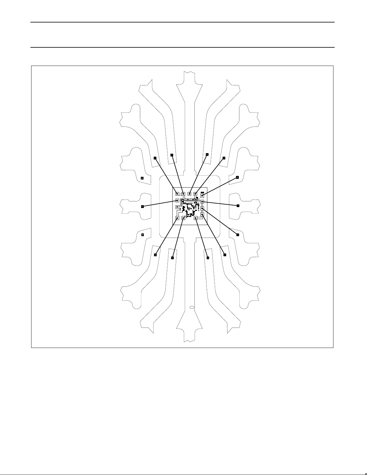
Figure 5. NE5210 Bonding Diagram
Die Sales Disclaimer
Due to the limitations in testing high frequency and other parameters
at the die level, and the fact that die electrical characteristics may
shift after packaging, die electrical parameters are not specified and
die are not guaranteed to meet electrical characteristics (including
temperature range) as noted in this data sheet which is intended
only to specify electrical characteristics for a packaged device.
All die are 100% functional with various parametrics tested at the
wafer level, at room temperature only (25°C), and are guaranteed to
be 100% functional as a result of electrical testing to the point of
wafer sawing only. Although the most modern processes are
utilized for wafer sawing and die pick and place into waffle pack
carriers, it is impossible to guarantee 100% functionality through this
process. There is no post waffle pack testing performed on
individual die.
Since Philips Semiconductors has no control of third party
procedures in the handling or packaging of die, Philips
Semiconductors assumes no liability for device functionality or
performance of the die or systems on any die sales.
Although Philips Semiconductors typically realizes a yield of 85%
after assembling die into their respective packages, with care
customers should achieve a similar yield. However, for the reasons
stated above, Philips Semiconductors cannot guarantee this or any
other yield on any die sales.
 Loading...