

Page 1
Philips Semiconductors Linear Products Product specification
NE50376-Bit A/D converter (parallel outputs)
582
August 31, 1994 853-0939 13721
DESCRIPTION
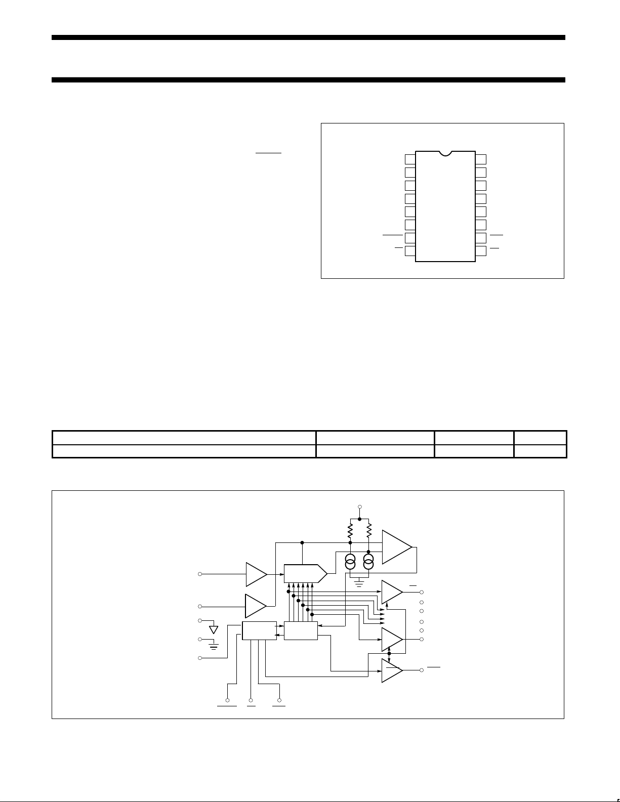
The NE5037 is a low cost, complete successive-approximation
analog-to-digital (A/D) converter, fabricated using Bipolar/I
2
L
technology. With an external reference voltage, the NE5037 will
accept input voltages between 0V and V
REF
. An external START
pulse of at least 300ns in duration will provide the 6-bit result of the
conversion in parallel format. Full conversion with no missing codes
occurs in 9µs.
FEATURES
•TTL-compatible inputs and outputs
•3-State output buffer
•Easy interface to CMOS microprocessors
•Fast conversion—9µs
•Guaranteed no missing codes over full temp range
•Single-supply operation, +5V
•Positive true binary outputs
•High-impedance analog inputs
APPLICATIONS
•Temperature control
PIN CONFIGURATION
1
2
3
4
5
6
7
8
9
10
11
12
13
14
16
15
N Package
V
CC
V
REF
V
IN
ANALOG GND
DIGITAL GND
CLK
START
CS
B5 (MSB)
B
3
B
4
B
2
B
1
B
0
EOC
EO
TOP VIEW
•µP-based appliances
•Light level monitors
•Head position sensing
•Electronic toys
•Joystick interface
ORDERING INFORMATION
DESCRIPTION TEMPERATURE RANGE ORDER CODE DWG #
16-Pin Plastic Dual In-Line Package (DIP) 0 to +70°C NE5037N 0406C
BLOCK DIAGRAM
V
REF
V
IN
A
GND
2
3
4
D
GND
CLK
5
6
CONTROL
LOGIC
SAR
V/I
V/I
7 8
9
I
IN
6–BIT
DAC
1/2
LSB
I
O
COM
DB
DB
EOC
DB
O
11
10
EOC
EOCCSSTART
16
DB
5
V
CC
1
Page 2
Philips Semiconductors Linear Products Product specification
NE50376-Bit A/D converter (parallel outputs)
August 31, 1994
583
ABSOLUTE MAXIMUM RATINGS
SYMBOL PARAMETER RATING UNIT
V
CC
Power supply voltage 7 V
V
REF
Reference voltage 7 V
V
IN(Analog)
Analog input voltage 7 V
V
IN(Digital)
Digital input voltage (CS, OE, START, CLK) 7 V
D
OUT
Data outputs (DB0 to DB5)
3-state mode 7 V
Enabled mode (each output) 5 mA
EOC End of conversion V
CC
∆
GND
Analog GND to digital GND ±1 V
T
A
Operating temperature range 0 to 70 °C
T
STG
Storage temperature range -65 to 150 °C
T
SOLD
Lead soldering temperature (10 seconds) 300 °C
P
D
Maximum power dissipation, TA=25°C (still-air)
1
N package 1450 mW
NOTES:
1. Derate above 25°C at the following rates:
N package=11.6mW/°C
DC ELECTRICAL CHARACTERISTICS
VCC=5.0V; V
REF
=2.0V; Clock=1MHz; 0°C ≤ T
A
≤ 70°C unless otherwise specified. Typical values are specified at 25°C
LIMITS
SYMBOL
PARAMETER
TEST CONDITIONS
Min Typ Max
UNIT
Resolution 6 6 6 Bits
Relative accuracy
1,2
1/4 1/2 LSB
V
CC
Positive supply voltage +4.75 +5.0 +5.50 V
ε
FS
Full-scale gain error
2,3,4
V
REF
=2.0V, TA=25°C ±1 ±2 LSB
ε
ZS
Zero-scale offset error
2
V
REF
=2.0V, TA=25°C ±1/2 -1/2, +2 LSB
PSR Power supply rejection, Max change in full-scale
2
V
REF
=2.0V, 4.75V≤VCC≤5.5V ±1/2 ±1 LSB
I
IN
Analog input bias current 0≤VIN≤2.5V 1 10 µA
I
REF
Reference bias current 0≤V
REF
≤2.5V 1 10 µA
R
IN
Analog input resistance 3 30 MΩ
V
IH
Logic ”1’ input voltage 2.0 V
V
IL
Logic ”0’ input voltage 0.8 V
I
IH
Logic ”1’ input current 10 µA
I
IL
Logic ”0’ input current 1 10 µA
I
OH
Logic ”1’ output current
5
2.4V≤V
OH
300 µA
I
OL
Logic ”0’ output current
5
VOL≤0.4V 1.6 mA
I
OZ
3-State leakage current ±0.1 ±40 µA
I
CC
Positive supply current 18 24 mA
P
D
Power dissipation 132 mW
NOTES:
1. Relative accuracy is defined as the deviation of the code transition points from the ideal code transition points on a straight line drawn from
zero-scale to full-scale of the device.
2. Specifications given in LSBs refer to the weight of the least significant bit at the 6-bit level which is 1.56% of the full-scale voltage.
3. Full-scale gain error is the deviation of the full-scale code transition point (111110 to 111111) from its ideal value.
4. The analog input voltage (V
IN
) range is 0V to V
REF
nominally, with the output remaining at 111111 even though the input may increase from
V
REF
to VCC. (For optimum performance, V
REF
can be any value from 1.5V to 2.5V.)
5. The data outputs have active pull-ups. The EOC
line is open-collector with a nominal 5kΩ internal pull-up resistor.
Page 3
Philips Semiconductors Linear Products Product specification
NE50376-Bit A/D converter (parallel outputs)
August 31, 1994
584
AC ELECTRICAL CHARACTERISTICS
VCC=5.0V; V
REF
=2.0V; Clock=1MHz; 0°C ≤ T
A
≤ 70°C unless otherwise specified. Typical values are specified at 25°C (Refer to AC test
figures.)
LIMITS
SYMBOL
PARAMETER
TO
FROM
TEST CONDITIONS
Min Typ Max
UNIT
f
MAX
Maximum clock frequency 1 MHz
t
W
Start pulse width 300 ns
Minimum positive/negative
clock pulse width
300 ns
t
CONV
Conversion time 9 Clock cycles
t
P (OUT DATA)
Propagation delay
1
Data out OE TA=25°C tR=tF≤20ns 500 ns
t
P (OUT EOC)
Propagation delay
2
EOC Clock TA=25°C tR=tF≤20ns 800 ns
t
P (3-STATE)
Propagation delay, 3-State 3-State Data OE TA=25°C tR=tF≤20ns 500 ns
NOTES:
1. Propagation delay of data outputs is defined as the delay in the data outputs reading their final value after the low going edge of OE.
2. Propagation delay of EOC
is defined as the delay in EOC going low, following the low going edge of the 9th clock pulse after the start pulse.
CIRCUIT DESCRIPTION
NE5037 is a complete 6-bit, parallel output, microprocessor
compatible, A/D converter which incorporates the
successive-approximation method. The chip includes the internal
control logic, the successive-approximation register (SAR), 6-bit
DAC, comparator and output buffers. An externally-generated clock
source (max frequency=1MHz) must be provided to Pin 6. An
external reference voltage supplied to Pin 2 sets the full-scale range
of the A/D converter.
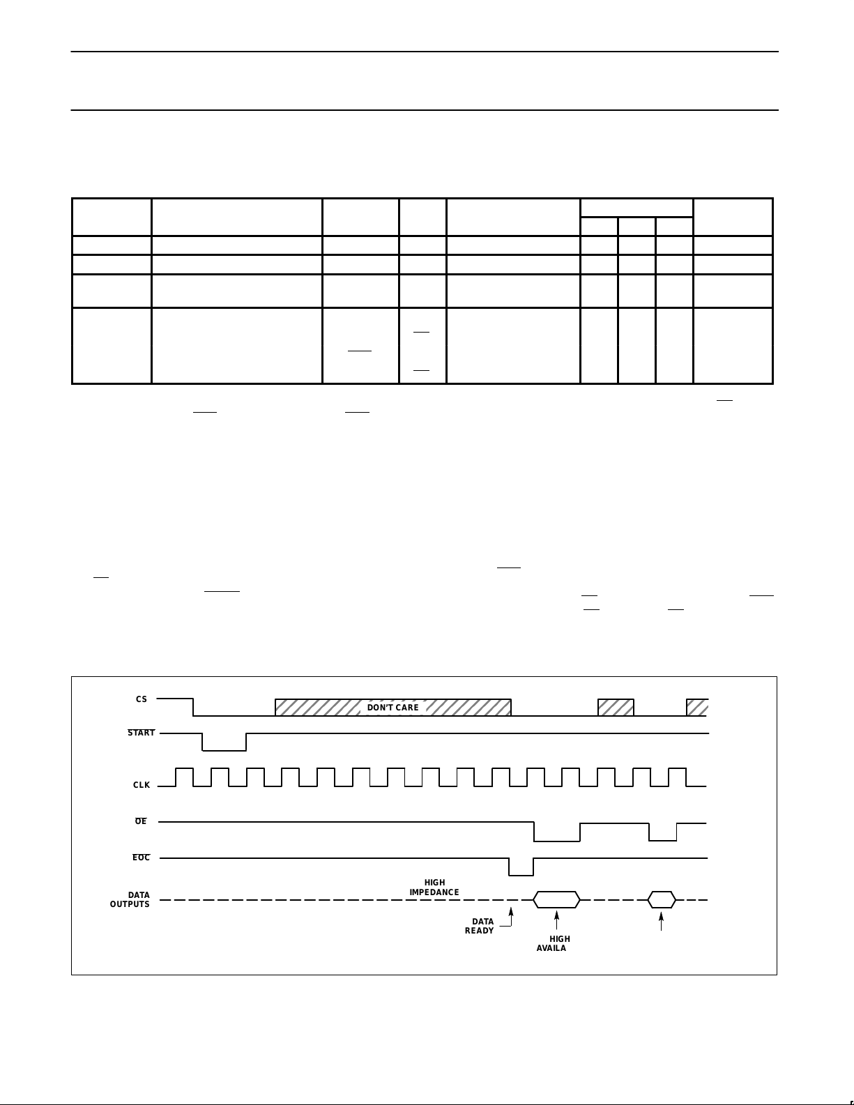
The CS
pin must be at a low level prior to the start of the conversion
process. Upon receipt of a START
pulse, the internal control logic
resets the SAR. On the first low-going edge of the clock pulse,
successive approximation conversion commences. Successive bits
beginning with the MSB (D5) are supplied to the input of the internal
6-bit current output DAC by the I
2
L successive approximation
register.
The comparator determines whether the output current of the DAC
is greater or less than the input current, which is converted from the
unknown analog input voltage through the V/I converter. If the DAC
output is greater, that bit of the DAC is set to ”0’ and the
corresponding output buffer goes to ”0’ simultaneously. If it is less, it
stays at ‘1’ and the output buffer also stays at ‘1’. On successive
clock pulses, successive bits of the DAC are tried and the
corresponding output buffer represents the bits of the DAC. On the
eighth low-going edge of the clock pulse (after the receipt of the start
pulse), the EOC
pin goes low, thereby indicating that the conversion
is complete. The output data is now valid. In order to access the
result of the conversion, the OE
pin must be set to a low level. EOC
is reset to a high state when OE is low. When OE is in a ”1’ state,
the output buffers are in a high impedance state.
Refer to Figure 1 for the timing diagram.
DON’T CARE
CS
START
CLK
OE
EOC
DATA
OUTPUTS
HIGH
IMPEDANCE
DATA
READY
HIGH
AVAILABLE
HIGH
IMPEDANCE
HIGH
IMPEDANCE
HIGH
AVAILABLE
Figure 1. Timing Diagram
Page 4
Philips Semiconductors Linear Products Product specification
NE50376-Bit A/D converter (parallel outputs)
August 31, 1994
585
TRANSFER CHARACTERISTICS
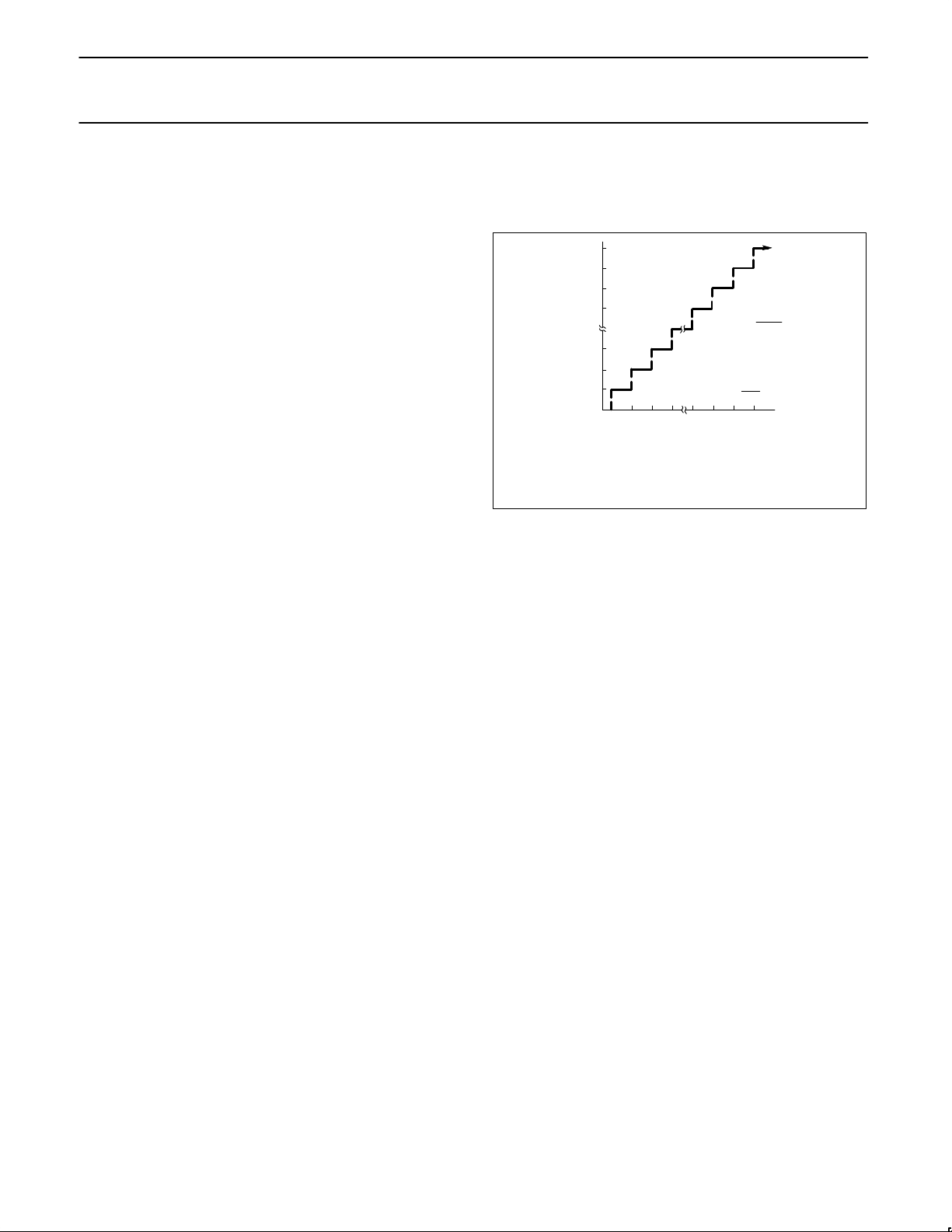
The ideal transfer characteristic of the NE5037 is shown in Figure 2.
The NE5037 is designed to have a nominal LSB offset so that the
code transition points are located LSB on either side of the exact
analog inputs for a given code.
Thus the first transition (000000 to 000001) will occur at an input of
LSB (15.63mV with a V
REF
of 2.0V). Subsequent transitions will
occur at nominal increments of 1 LSB. The last transition (to
full-scale—111111) will occur at 62.5 LSB (1.953V at V
REF
of 2.0V).
LAYOUT PRECAUTIONS
Analog ground (Pin 4) and digital ground (Pin 5) are not connected
internally and should be connected together as close to the device
as possible for optimum performance. The circuit will operate with as
much as ±200mV between the two grounds but some degradation
will occur. The leads to the analog inputs should be kept as short as
possible to minimize noise pick-up. Input bypass capacitors from the
analog inputs to ground will eliminate noise pick-up. Power supplies
should be decoupled with at least 1µF located close to the device to
minimize the effects of noise spikes.
The reference input and the analog voltage input must both remain
stable during conversion to insure accuracy and proper operation.
This can be done by adequately bypassing these inputs and/or
keeping the impedance of these inputs at or below 2kΩ.
111111
111110
111101
111100
000011
000010
000001
000000
1/2 LSB
3/2 LSB
5/2 LSB
7/2 LSB
119/2 LSB
121/2 LSB
123/2 LSB
125/2 LSB
1DIGITAL OUTPUT CODE
ANALOG INPUT
LSB
V
REF
64
62.5LSB
62.5
64
V
REF
FOR 111111 OUTPUT
V
IN
= V
REF
— LSB — 1/2 LSB
BUILT–IN OFFSET
Figure 2. Ideal Transfer Characteristics
Page 5
Philips Semiconductors Linear Products Product specification
NE50376-Bit A/D converter (parallel outputs)
August 31, 1994
586
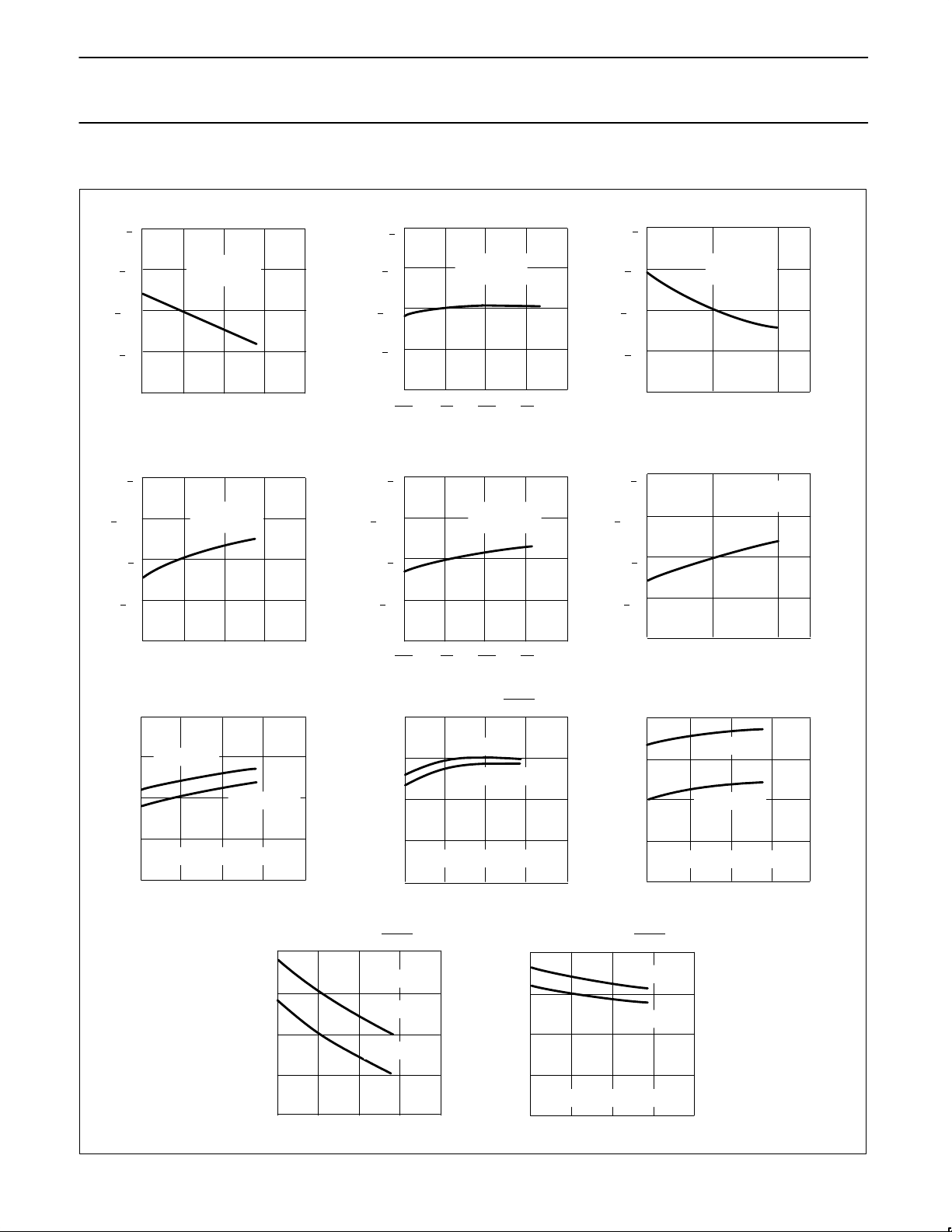
TYPICAL PERFORMANCE CHARACTERISTICS
4
3
2
1
0
+1
+
3/4
+
31/2
+
1/4
0
0
25 50 75
VCC = 5.0V
V
REF
= 2.0V
T
A
(oC)
Z–F OFFSET ERROR (LSB’s)
+1
+3/4
+
31/2
+
1/4
0
4.75
5.0 5.25 5.5
Z–F OFFSET ERROR (LSB’s)
V
REF
= 2.0V
T
A
= 25oC
V
CC
(VOLTS DC)
VCC = 5.0V
T
A
= 25oC
+
1
+
3/4
+
31/2
+
1/4
0
Z–F OFFSET ERROR (LSB’s)
1.5 2.0 2.5
V
REF
(VOLTS DC)
+
2
+1 1/2
+1
+
1/2
0
0 25 50 75
T
A
(oC)
Z–F GAIN ERROR (LSB’s)
VCC = 5.0V
V
REF
= 2.0V
Z–F GAIN ERROR (LSB’s)
+2
+1 1/2
+1
+
1/2
0
4.75
5.0 5.25 5.5
VCC (VOLTS DC)
V
REF
= 2.0V
T
A
= 25oC
Z–F GAIN ERROR (LSB’s)
+2
+1 1/2
+1
+
1/2
0
VCC = 5.0V
T
A
= 25oC
1.5 2.0 2.5
V
REF
(VOLTS DC)
VCC = 4.75V
VCC = 5.0V
IOL @ VOL = 0.4V
DC
4
3
2
1
0
0 25 50 75
I (mA)
OL
TA (oC)
I (mA)
OL
0 25 50 75
T
A
(oC)
VCC = 5.0V
VCC = 4.75V
IOL @ VOL = 0.4V
DC
VCC = 5.0V
VCC = 4.75V
IOL @ VOL = 2.4V
DC
0 25 50 75
T
A
(oC)
I (mA)
OH
10.0
9.0
8.0
7.0
6.0
I (mA)
CC
V
REF
= 2.0V
VCC = 5.5V
VCC = 4.75V
0 25 50 75
T
A
(oC)
4
17
16
15
14
13
0 25 50 75
T
A
(oC)
VCC = 5.0V
VCC = 4.75V
IOH @ VOH = 2.4V
DC
I (mA)
OH
0.5
0.4
0.3
0.2
0.1
Zero–Scale Offset Error vs Temp Zero–Scale Offset Error vs v
cc
Zero–Scale Offset Error vs v
REF
Full–Scale GAIN Error vs Temp Full–Scale Gain Error vs v
cc
Full–Scale Gain Error vs v
REF
IOL vs Temp (Data Output) IOH vs Temp (Data Output)
I
CC
vs Temp (EOC) IOH vs Temp (EOC)
I
OL
vs Temp (EOC)
Page 6
Philips Semiconductors Linear Products Product specification
NE50376-Bit A/D converter (parallel outputs)
August 31, 1994
587
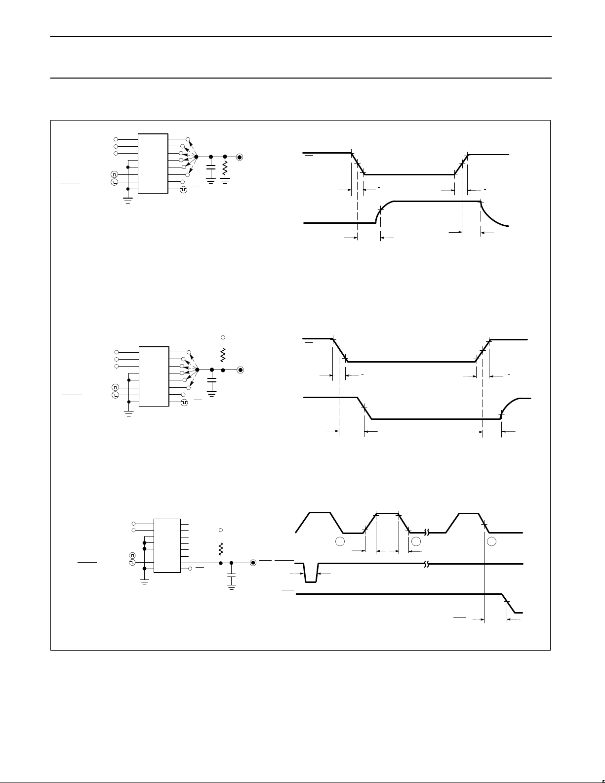
AC TEST CIRCUITS AND WAVEFORMS
Propagation Delay Time EOC t
P(EOC)
VCC = 5V
V
REF
= 2V
V
IN
= 2.1V
1MHz CLK (TTL)
EO (TTL LEVEL)
15pF
10kΩ
DATA OUTPUT
NE5037
VCC = 5V
V
REF
= 2V
VIN = 0.1V
1MHz CLK (TTL)
EO (TTL LEVEL)
15pF
10K
DATA OUTPUT
NE5037
VCC = +5V
VCC = +5V
V
REF
= +2V
1MHz TTL (CLOCK)
START
PULSE
(TTL LEVEL)
EO
= V
CC
NE5037
V
CC
10kΩ
OE
90%
50%
10%
t
F
50%
tp (DATA)
DB (0 TO 5)
1R = tF = 20ns
t
R
tp (3–STATE)
10%
50%
90%
t
R
10%
GND
GND
V
CC
t
F
50%
50%
V
CC
V
CC
tp (DATA)
OE
DB (0 TO 5)
tp (3–STATE)
90%
10%
90%
10%
t
R
t
F
CLK
1 2
EOC
START
EOC
t
W
50%
50%
tp (EOC
)
9
1R = tF = 20ns
tp (DATA)
10%
START
PULSE
(TTL LEVEL)
START
PULSE
(TTL LEVEL)
90%
50%
10%
Data Output High
Propagation Delay Time t
P
(DATA) and TP (3-state)
Page 7
Philips Semiconductors Linear Products Product specification
NE50376-Bit A/D converter (parallel outputs)
August 31, 1994
588
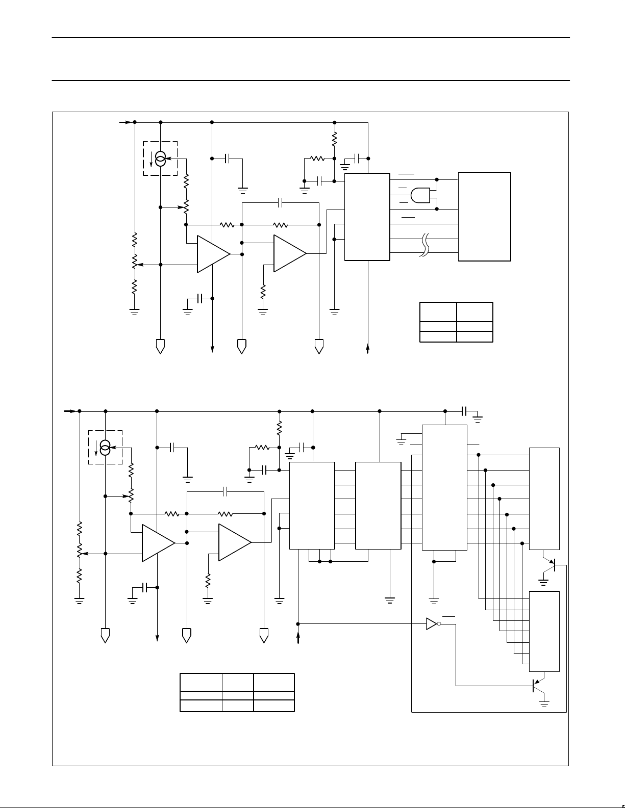
a. Temperature Sensor
b. Digital Thermometer
+5V
LM334
0.1µF
160
RANGE
100
5.76K (F)
3.2 K (C)
1/2
NE5512
8
2
3
4
–
+
1K
BIAS
ADJ.
1K
820
0.1µF
220
330
0.1µF
0.1µF
2
1
3
4
5
1000pF
10K
6
5
910
1/2
NE5512
7
–
+
NE5037
A/D
6
7 STRT
8 CS
9 OE
10 EOC
11–16
CONTROLLER
6–BIT
DATA BUS
DISPLAY
READING
VOLTAGE
TP1
o
F
o
C
1.5895
0.8742
CLKTP3TP2–3VTP1*
+5V
LM334
0.1µF
160
RANGE
100
5.76K (F)
3.2 K (C)
1/2
NE5512
8
2
3
4
–
+
1K
BIAS
ADJ.
1K
820
0.1µF
220
330
0.1µF
0.1µF
2
1
3
4
5
1000pF
10K
6
5
910
1/2
NE5512
7
–
+
NE5037
A/D
CLKTP3TP2–3VTP1*
N74LS174
6–BIT
LATCH
N82S147
PROM
(DECODER/
DRIVER)
19
18
17
16
5
4
3
2
1
16
15
14
13
12
11 11
6
13
4
3
14
6 7 9 10 9 8 10 15
20
14
13
12
11
9
8
7
6
OPEN
0.22µF
DIS 1
10’s
DIS 2
10’s
Q1
2N3906
Q2
2N3986
CLK
DISPLAY
READING
VOLTAGE
TP1
o
F
o
C
1.5895
0.8742
U7
PIN 18
GND
HIGH
5
12
7
10
2
15
Figure 3.
Page 8

Philips Semiconductors Linear Products Product specification
NE50376-Bit A/D converter (parallel outputs)
August 31, 1994
589
APPLICATION
•0 to 63°C Temperature Sensor
CIRCUIT DESCRIPTION
The temperature sensor of Figure 3 provides an input to Pin 3 of the
NE5037 of 32mV/°C. This 32mV is the value of one LSB for the
NE5037. The LM334 is a three-terminal temperature sensor and
provides a current of 1µA for each °Kelvin. The first section of the
dual op amp is connected as a trans-impedance amplifier to convert
the current from the LM334 to a voltage, which is amplified and
inverted by the section amplifier. Note that the first amplifier requires
different values of feedback resistance for °C and °F. The NE5512
was chosen for its low temperature coefficient of input bias current
as excessive I
OS
tempco would degrade temperature tracking.
To read temperature, conversion is started by sending a momentary
low signal to Pin 7 of the NE5037. When Pin 10 of the NE5037 goes
low, conversion is complete and a low is applied to Pin 9 of the
NE5037 to read data on Pins 11 through 16. Note that this
temperature data is in straight binary format.
The controller can be a microprocessor in a temperature control
application, or discrete circuitry in a simple temperature reporting
application. A temperature reporting (digital thermometer) circuit is
shown in Figure 3b. The NE5037 A/D converter is connected in a
continuous conversion mode by connecting together Pins 7, 9, and
10. Should this pin be momentarily shorted to any relatively low
impedance point, conversion will stop. Conversion will resume upon
interruption and restoration of the power. These pins are also
connected to the latch enable of a 6-bit latch because the data at the
converter output is available for only a short time when the converter
is in the continuous conversion mode. The (P)ROM) must have the
correct code for converting the data from the NE5037 (used as
address for the (P)ROMs) to the appropriate segment drive codes.
Note that the circuit of Figure 3b shows a circuit which can be used
to display either Fahrenheit or Centigrade temperatures.
The displayed output could easily be converted to degrees
Fahrenheit (°F) by the controller of Figure 3a or through the
(P)ROMs of Figure 3b. When doing this, a third (hundreds) digit
(P)ROM and display will be needed for displaying temperatures
above 99°F.
An inexpensive clock can be made from NAND gates or inverters,
as shown in Figure 3c.
CIRCUIT ADJUSTMENT
The circuit should be at a known ambient temperature for a few
minutes before making adjustments.
14.Adjust bias adjust potentiometer for the voltage indicated in the
chart in Figure 3b.
15.With the circuit (or sensor U3, if it is remotely located) at a known
temperature for 2 to 3 minutes, adjust range control for a correct
reading on the displays.
This should provide an accuracy of ±3 counts (3° F or C). Higher
accuracy may require NE5037 reference voltage regulation.
 Loading...