

Page 1
Philips Semiconductors Linear Products Product specification
NE502010-Bit µP-compatible D/A converter
757
August 31, 1994 853-0392 13721
DESCRIPTION
The NE5020 is a microprocessor-compatible monolithic 10-bit
digital-to-analog converter subsystem. This device offers 10-bit
resolution and ±0.1% accuracy and monotonicity guaranteed over
full operating temperature range.
Low loading latches, adjustable logic thresholds, and addressing
capability allow the NE5020 to directly interface with most
microprocessor- and logic-controlled systems.
The NE5020 contains internal voltage reference, DAC switches and
resistor ladder. Also, the input buffer and output summing amplifier
are included. In addition, the matched application resistors for
scaling either unipolar or bipolar output values are included on a
single monolithic chip.
The result is a near minimum component count 10-bit resolution
DAC system.
FEATURES
•10-bit resolution
•Guaranteed monotonicity over operating range
•±0.1% relative accuracy
•Unipolar (0V to +10V) and bipolar (± 5V) output range
•Logic bus compatible
•5µs settling time
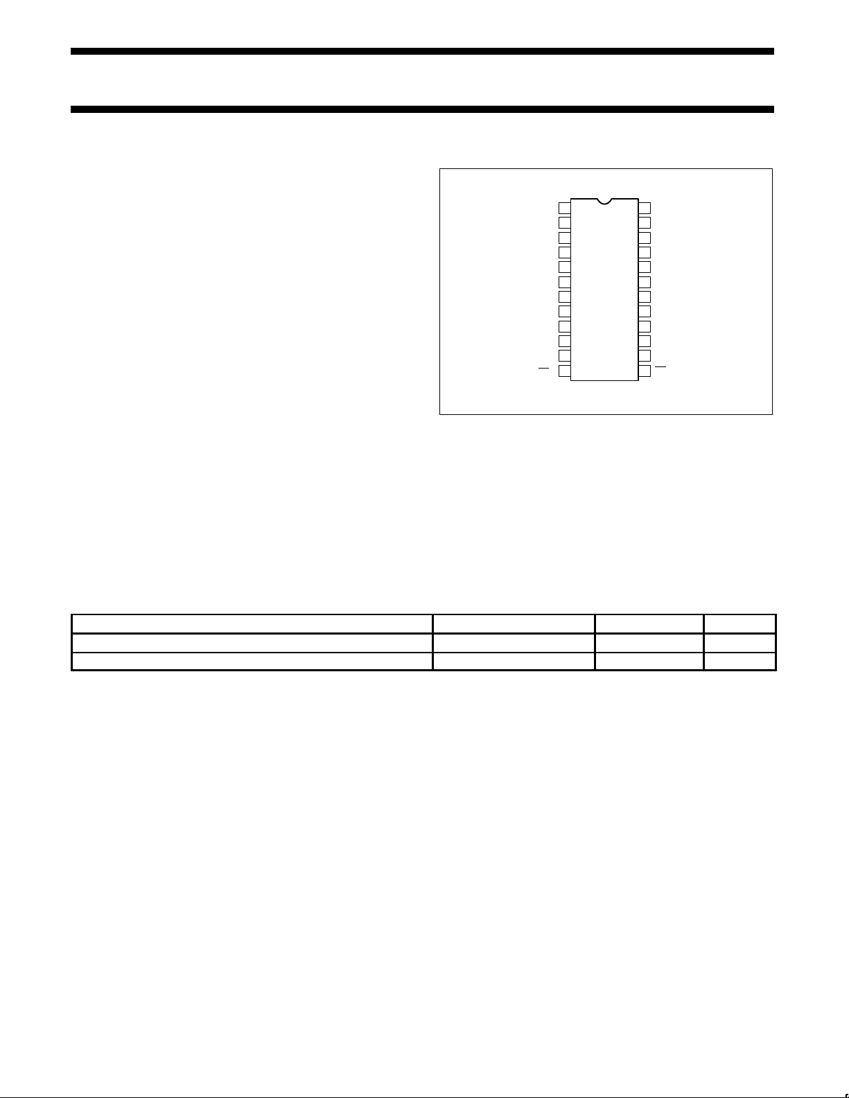
PIN CONFIGURATION
1
2
3
4
5
6
7
8
9
10
11
12
13
14
24
23
22
21
20
19
18
17
16
15
F, N Packages
DIGITAL GND
DB0(LSB)
DB1
DB2
DB3
DB4
DB5
DB6
DB7(MSB)
NC
ANALOG GND
AMP COMP
SUM MODE
BIPOLAR OFFSET R
LE
1
V
CC+
V
OUT
V
CC–
+V
REF
IN
V
REF
OUT
–V
REF
IN
V
REF
ADJ
LE
2
APPLICATIONS
•Precision 10-bit D/A converters
•10-bit analog-to-digital converters
•Programmable power supplies
•Test equipment
•Measurement instruments
ORDERING INFORMATION
DESCRIPTION TEMPERATURE RANGE ORDER CODE DWG #
24-Pin Ceramic Dual In-Line Package (CERDIP) 0 to 70°C NE5020F 0588B
24-Pin Plastic Dual In-Line Package (DIP) 0 to 70°C NE5020N 0412A
Page 2
Philips Semiconductors Linear Products Product specification
NE502010-Bit µP-compatible D/A converter
August 31, 1994
758
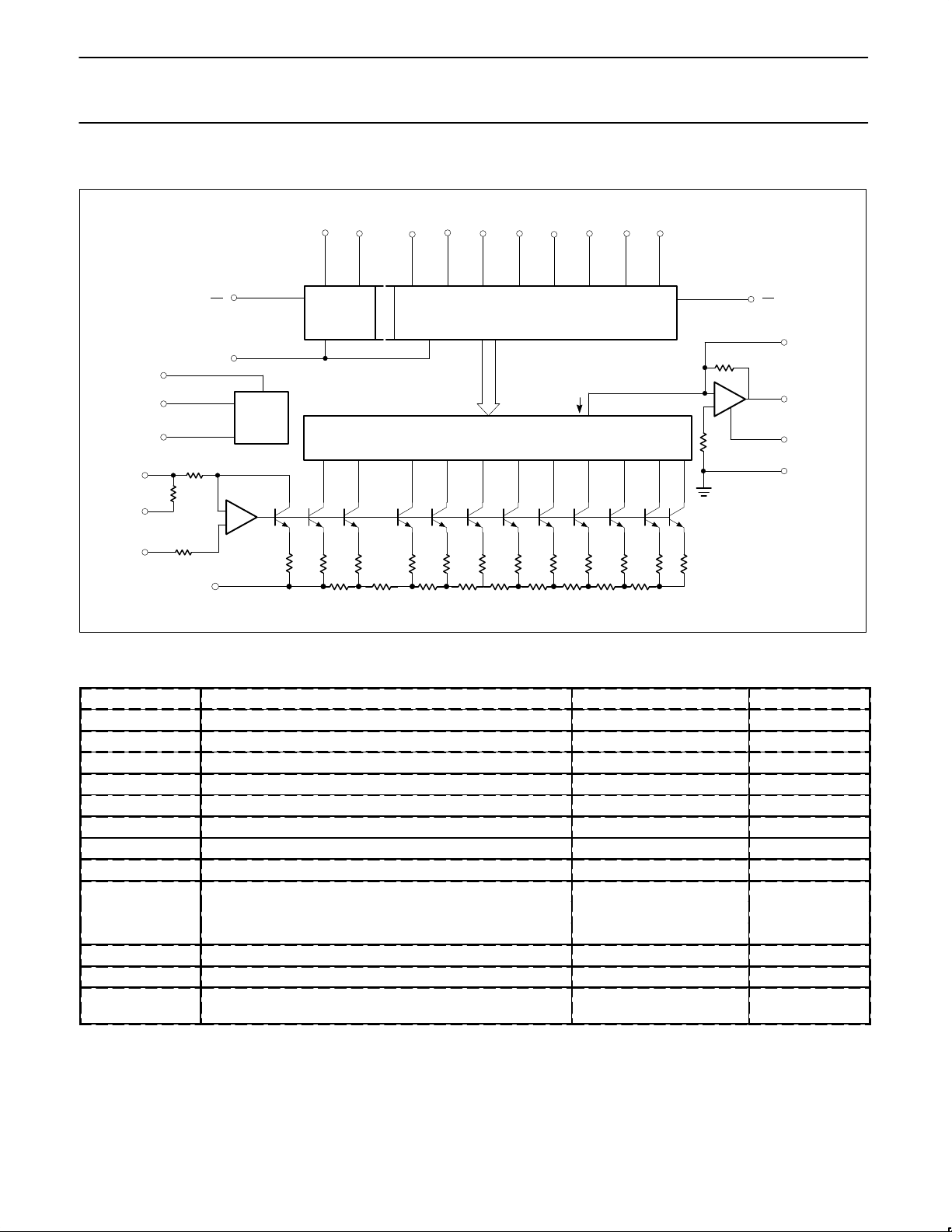
BLOCK DIAGRAM
(15)
(14)
(22)
(20)
(23)
(24)
(17)
(18)
BIPOLAR
OFFSET
+V
REF
IN
ANALOG
GND
AMP
COMP
SUM
NODE
DAC OUTPUT CURRENT
DAC SWITCHES
(19)
(13)
MSB
LSB
DIGITAL GND(1)
–V
CC
INT
V
REF
(11)
DB9
(10)
DB8
(9)
DB7
(8)
DB6
(7)
DB5
(6)
DB4
(5)
DB3
(4)
DB2
LE
2
V
OUT
+
–
V
REF
OUT
V
REF
ADJ
+
–
QRQ9Q
8
Q7Q6Q5Q4Q3Q2Q1Q
0
Q
T
(3)
DB1
(2)
DB0
LATCHES AND
SWITCH DRIVERS
(12)
LE
1
(21)
+V
CC
R
BIP
R
REF
R
(16)
–V
REF
IN
R
R
fb
ABSOLUTE MAXIMUM RATINGS
SYMBOL PARAMETER RATING UNIT
V
CC
+
Positive supply voltage 18 V
V
CC
-
Negative supply voltage -18 V
V
IN
Logic input voltage 0 to 18 V
V
REF IN
Voltage at +V
REF
input 12 V
V
REF ADJ
Voltage at V
REF
adjust 0 to V
REF
V
V
SUM
Voltage at sum node 12 V
I
REFSC
Short-circuit current to ground at V
REF OUT
Continuous
I
OUTSC
Short-circuit current to ground or either supply at V
OUT
Continuous
P
D
Maximum power dissipation TA=25°C, (still-air)
1
F package 2150 mW
N package 2150 mW
T
A
Operating temperature range NE5020 0 to +70 °C
T
STG
Storage temperature range -65 to +150 °C
T
SOLD
Lead soldering temperature
(10 sec. max)
300 °C
NOTES:
1. Derate above 25°C at the following rates:
F package at 17.2mW/°C
N package at 17.2mW/°C
Page 3

Philips Semiconductors Linear Products Product specification
NE502010-Bit µP-compatible D/A converter
August 31, 1994
759
DC ELECTRICAL CHARACTERISTICS
VCC+=+15V, VCC-=-15V, 0 ≤ TA≤70°C, unless otherwise specified.1 Typical values are specified at 25°C.
LIMITS
SYMBOL
PARAMETER
TEST CONDITIONS
Min Typ Max
UNIT
Resolution
Monotonicity
Relative accuracy
10
10
±0.1
Bits
Bits
%FS
V
CC+
V
CC-
Positive supply voltage
Negative supply voltage
11.4
-11.415-15
16.5
-16.5
V
V
V
IN(1)
V
IN(0)
Logic “1” input voltage
Logic “0” input voltage
Pin 1=0V
Pin 1=0V
2.0
0.8
V
V
I
IN(1)
I
IN(0)
Logic “1” input current
Logic “0” input current
Pin 1=0V, 2<VIN<18V
Pin 1=0V, -5V<V
IN
<0.8V
0.1
-2.010-10
µA
µA
V
FS
Full-scale output
Unipolar mode, V
REF
=5.000V, all bits high,
T
A
=25°C
9.5 10.5 V
+V
FS
Full-scale output Bipolar mode, V
REF
=5.000V, all bits high, TA=25°C 4.75 5.25 V
-V
FS
Negative full-scale Bipolar mode, V
REF
=5.000V, all bits low, TA=25°C -5.25 -4.75 V
NOTES:
1. Refer to Figure 1.
Page 4
Philips Semiconductors Linear Products Product specification
NE502010-Bit µP-compatible D/A converter
August 31, 1994
760
DC ELECTRICAL CHARACTERISTICS (Continued)
LIMITS
SYMBOL
PARAMETER
TEST CONDITIONS
Min Typ Max
UNIT
V
ZS
Zero-scale output Unipolar mode, V
REF
=5.000V, all bits low, TA=25°C -30 +30 mV
I
OS
Output short-circuit current TA=25°C
V
OUT
=0V
±15 ±40 mA
PSR+
(OUT)
Output power supply rejection (+) V-=-15V, 13.5V≤V+≤16.5V, external
V
REF IN
=5.000V
0.001 0.01 %FS/
%VS
PSR-
(OUT)
Output power supply rejection (-) V+=15V, -13.5V≤V-≤-16.5V, external
V
REF IN
=5.000V
0.001 0.01 %FS/
%VS
TC
FS
Full-scale temperature coefficient V
REF IN
=5.000V 20 ppmFS
/°C
TC
ZS
Zero-scale temperature coefficient 5 ppmFS/°C
I
REF
2
Reference output current 3 mA
I
REF SC
Reference short circuit current TA=25°C
V
REF OUT
=0V
15 30 mA
PSR+
REF
Reference power supply rejection
(+)
V-=-15V, 13.5V≤V+≤16.5V, I
REF
=1.0mA .003 .01 %VR/
%VS
PSR-
REF
Reference power supply rejection
(-)
V+=15V, -13.5V≤V-≤16.5V, .003 .01 %VR/
%VS
V
REF
Reference voltage I
REF
=1.0mA, TA=25°C 4.9 5.0 5.25 V
TC
REF
Reference voltage temperature coefficient
I
REF
=1.0mA 60 ppm/°C
Z
IN
DAC V
REF IN
input impedance I
REF
=1.0mA 5.0 kΩ
ICC+ Positive supply current VCC+=15V 7 14 mA
ICC- Negative supply current VCC-=-15V -10 -15 mA
P
D
Power dissipation I
REF
=1.0mA, VCC=±15V 255 435 mW
NOTES:
1. Refer to Figure 1.
2. For I
REF OUT
greater than 3mA, an external buffer is required.
AC ELECTRICAL CHARACTERISTICS
1
V
CC
= +15V, T
A
= 25°C.
LIMITS
SYMBOL
PARAMETER
TO
FROM
TEST CONDITIONS
Min Typ Max
UNIT
t
SLH
Settling time ±1/2LSB Input All bits low-to-high
2
5 µs
t
SHL
Settling time ±1/2LSB Input All bits high-to-low
3
5 µs
t
PLH
Propagation delay Output Input All bits switched low-to-high
2
30 ns
t
PHL
Propagation delay Output Input All bits switched high-to-low
3
150 ns
t
PLSB
Propagation delay Output Input 1 LSB change
2,3
150 ns
t
PLH
Propagation delay Output LE Low-to-high transition
4
300 ns
t
PHL
Propagation delay Output LE High-to-low transition
5
150 ns
t
S
Set-up time LE Input
1,6
100 ns
t
H
Hold time Input LE
1,6
50 ns
t
PW
Latch enable pulse width
1,6
150 ns
NOTES:
1. Refer to Figure 2.
2. See Figure 5.
3. See Figure 6.
4. See Figure 7.
5. See Figure 8.
6. See Figure 9.
Page 5
Philips Semiconductors Linear Products Product specification
NE502010-Bit µP-compatible D/A converter
August 31, 1994
761
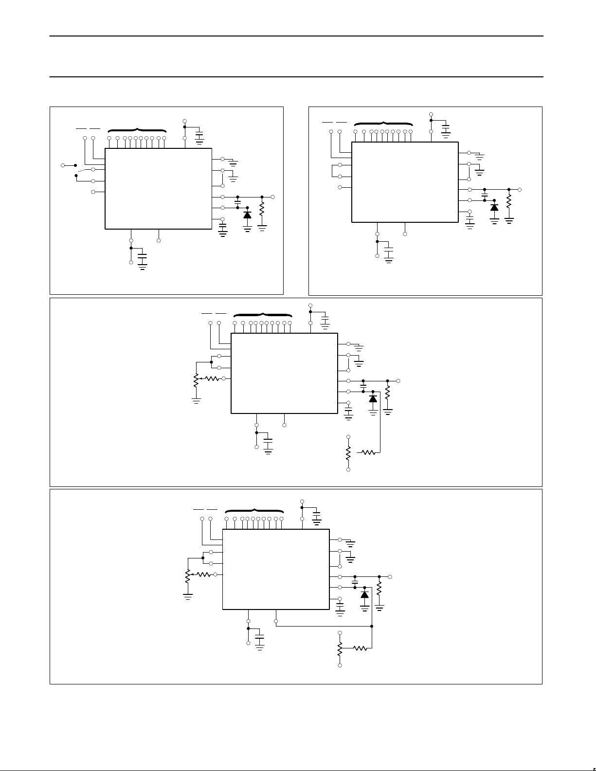
Figure 1. DC Parametric Test Configuration
0.47µF
MSB LSB
1110 98 7 6 5 4 21
1
24
20
22
23
1819
14
15
17
12
5020
COMP
AMP
SUM
ANA GND
DIG GND
LE1
V
REF
IN
V
REF
OUT
V
OUT
V
CC+
0.1µF
V
CC–
OUTPUT
5k
30pF
100pF
5.000V
LE2
13
16
–V
REF
IN
3 2
Figure 2. AC Parametric Test Configuration
MSB LSB
1110 98 7 6 5 4 21
1
24
20
22
23
1819
14
15
17
12
5020
COMP
AMP
SUM
ANA GND
DIG GND
13
16
3 2
0.47µF
LE1
V
OUT
V
CC+
0.1µF
V
CC–
LE2
–V
REF
IN
OUTPUT
5k
30pF
100pF
Figure 3. Full-/Zero-Scale Adjust — Unipolar Output (0–10V)
MSB LSB
1110 98 7 6 5 4 21
1
24
20
22
23
1819
14
15
17
12
5020
COMP
AMP
SUM
ANA GND
DIG GND
13
16
3 2
0.47µF
LE1
V
REF
IN
V
REF
OUT
V
OUT
V
CC+
0.1µF
V
CC–
LE2
–V
REF
IN
10k
10T
80k
FULL SCALE
ADJUST
V
REF
ADJ
OUTPUT
5k
30pF
100pF
1M
V
CC+
20k
10T
ZERO SCALE
ADJUST
V
CC–
Figure 4. Bipolar Output Operation (–5 to +5V)
MSB LSB
1110 9 8 7 65 4 21
1
24
20
22
23
1819
14
15
17
12
5020
COMP
AMP
SUM
ANA GND
DIG GND
13
16
3 2
0.47µF
LE1
V
REF
IN
V
REF
OUT
V
OUT
V
CC+
0.1µF
V
CC–
LE2
–V
REF
IN
10k
10T
80k
V
REF
ADJ
OUTPUT
5k
30pF
100pF
1M
V
CC+
20k
10T
FULL SCALE
ADJUST
V
CC–
BIP OFF
Page 6
Philips Semiconductors Linear Products Product specification
NE502010-Bit µP-compatible D/A converter
August 31, 1994
762
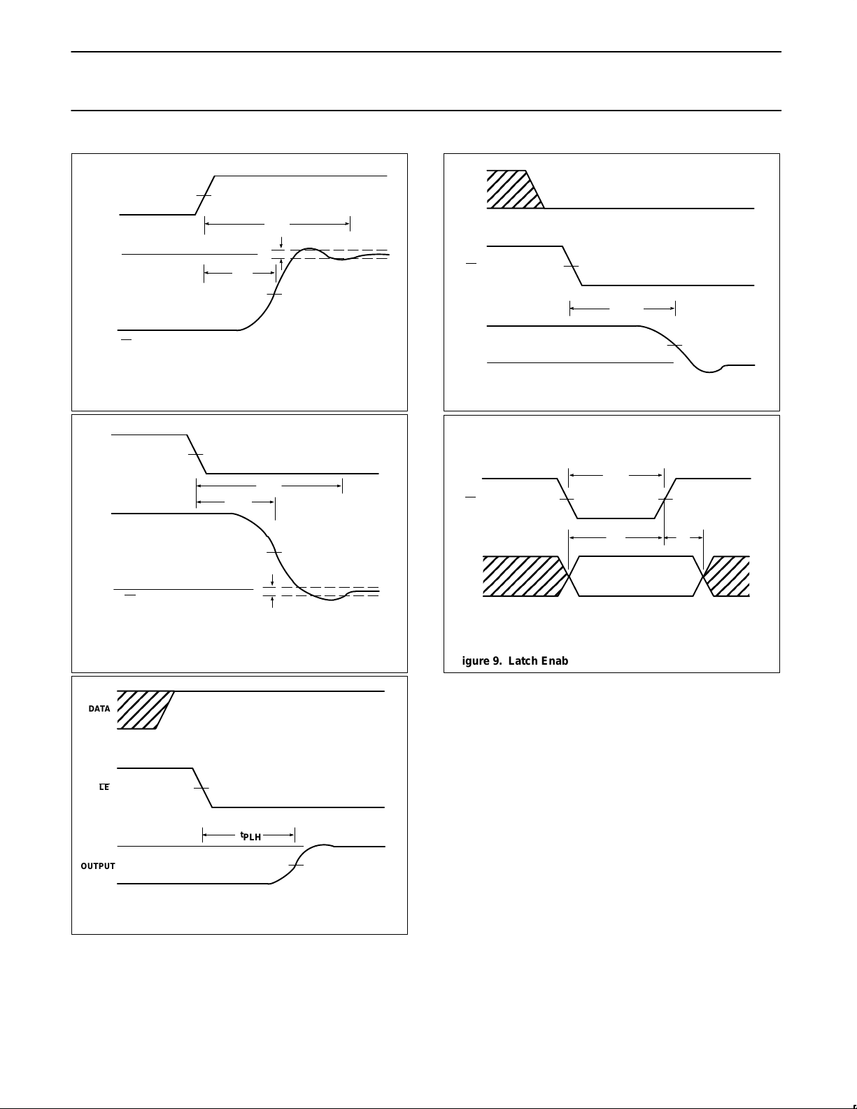
Figure 5. Settling Time and Propagation Delay,
Low-to-High Data
OUTPUT
t
SLH
t
PLH
1LSB
DATA
10V
0V
LE
= LOW
Figure 6. Settling Time and Propagation Delay,
High-to-Low Data
LE = LOW
t
SHL
OUTPUT
10V
0V
1LSB
t
PHL
DATA
Figure 7. Propagation Delay, Latch Enable to Output
LE
DATA
t
PLH
OUTPUT
10V
0V
Figure 8. Propagation Delay, Latch Enable to Output
LE
DATA
t
PHL
t
PHL
OUTPUT
10V
0V
Figure 9. Latch Enable Pulse Width, Setup and Hold Times
LE
DATA
t
MIN
t
S
t
h
Page 7
Philips Semiconductors Linear Products Product specification
NE502010-Bit µP-compatible D/A converter
August 31, 1994
763
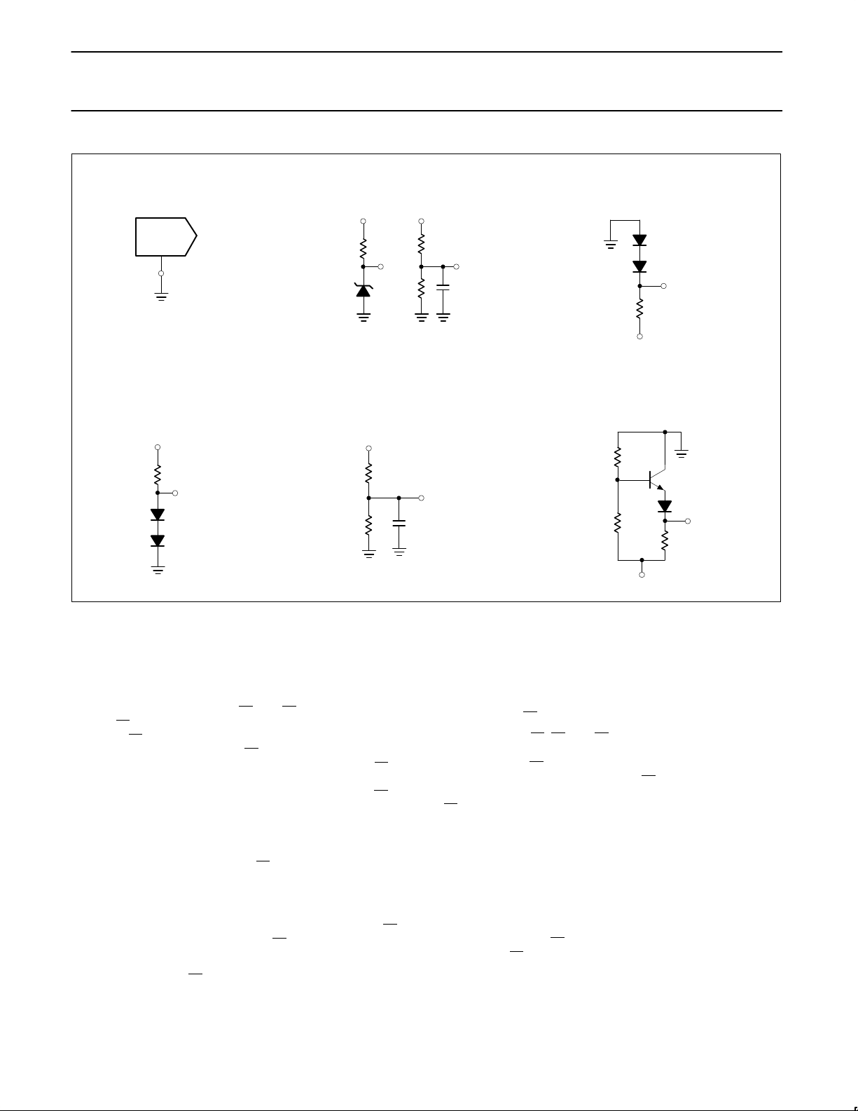
Figure 10.
NE5020
DIG GND (PIN 1)
+5V
PIN 1
IN4148
3.6kΩ
3.6kΩ
6.2kΩ
+10V
PIN 1
0.1µF
PIN 1
IN4148
2N3904
1.3kΩ
3.9kΩ
1kΩ
IN4148
PIN 1
10kΩ
–5V TO –10V
NOTE: DO NOT EXCEED NEGATIVE
LOGIC INPUT RANGE OF DAC
6.2V
ZENER
10kΩ
9.1kΩ
PIN 1 PIN 1
0.1µF
6.2kΩ
+12V TO +15V
+15V
10k ECL
V
TH
≥ –1.29V
+10V CMOS
VTH = +9.0V
+5V CMOS
VTH = +2.8V
TTL,
DTL V
TH
= +1.4V
V
TH
= V
PIN1
+ 1.4V
+15V CMOS, HTL, HNIL
V
TH
= +7.6V
PMOS
V
TH
= 0V
CIRCUIT DESCRIPTION
The NE5020 provides ten data latches, an internal voltage
reference, application resistors, and a scaled output voltage in
addition to the basic DAC components (see Block Diagram).
Latch Circuit
Digital interface with the NE5020 is readily accomplished through
the use of two latch enable ports (LE
1
and LE2) and ten data input
latches. LE
2
controls the two most significant bits of data (DB9 and
DB8) while LE
1
controls the eight lesser significant bits (DB7 through
DB
0
). Both the latch enable ports (LE) and the data inputs are
static- and threshold-sensitive. When the latch enable ports (LE
)
are high (Logic ‘1’) the data inputs become very high impedances
and essentially disappear from the data bus. Addressing the LE
with a low static (Logic ‘0’), the latches become active and adapt the
logic states present on the data bus. During this state, the output of
the DAC will change to the value proportional to the data bus value.
When the latch enable returns to a high state, the selected set of
data inputs (i.e., depending on which LE
goes high) ‘memorizes’ the
data bus logic states and the output changes to the unique output
value corresponding to the binary word in the latch.
The data inputs are inactive and high impedance (typically requiring
–2µA for low (0.8V max) or 0.1µA for high (2.0V min) when the LE
is
high. Any changes on the data bus with LE
high will have no effect
on the DAC output.
The digital logic inputs (LE
and DB) for the NE5020 utilize a
differential input logic system with a threshold level of +1.4V with
respect to the voltage level on the digital ground pin (Pin 1). Figure
10 details several bias schemes used to provide the proper
threshold voltage levels for various logic families.
To be compatible with a bus-oriented system, the DAC should
respond in as short a period as possible to insure full utilization of
the microprocessor, controller and I/O control lines. Figure 9 shows
the typical timing requirements of the latch and data lines. This
figure indicates that data on the data bus should be stable for at
least 50ns after LE
is changed to a high state.
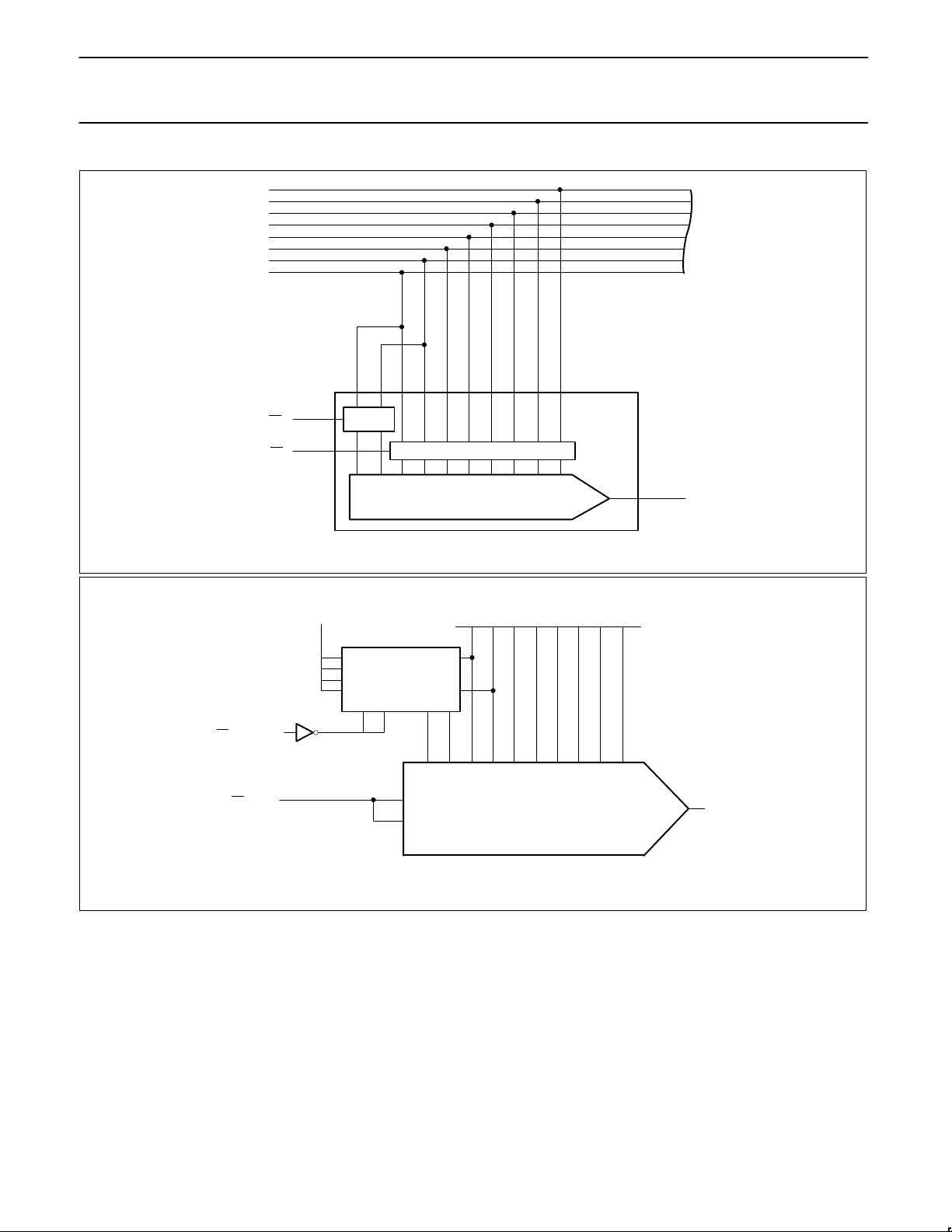
The independent LE
(LE1 and LE2) lines allow for direct interface
from an 8-bit bus (see Figure 11). Data for the two MSBs is supplied
and stored when LE
2
is activated low and returned high according to
the NE5020 timing requirements. Then LE
1
is activated low and the
remaining eight LSBs of data are transferred into the DAC. With
LE
1
returning high, the loading of 10-bit data word from an 8-bit data
bus is complete.
Occasionally the analog output must change to its data value within
one data address operation. This is no problem using the NE5020
on a 16-bit bus or any other data bus with 10 or greater data bits.
This can be accomplished from an 8-bit data bus by utilizing an
external latch circuit to pre-load the two MSB data values. Figure 12
shows the circuit configuration.
After pre-loading (via LE
pre-load) the external latch with the two
MSB values, LE
2
is activated low and the eight LSBs and the two
MSBs are concurrently loaded into the DAC in one address
operation. This permits the DAC output to make its appropriate
change at one time.
Page 8
Philips Semiconductors Linear Products Product specification
NE502010-Bit µP-compatible D/A converter
August 31, 1994
764
Figure 11. NE5020 µP Interface 8-Bit Data Bus Example
LATCHES
DAC
OUTPUT
LSBMSB
DB 9 8 7 6 5 4 3 2 1 0
DATA BUS
B0
B6
B7
LE
2
LE
1
LATCHES
Figure 12. Pre-loading the 2 MSBs to Provide a Single-Step Output
+5V
8-BIT DATA BUS
74LS74
1
4
10
13
2
12
3 11 5 9
11 10 9 8 7 6 5 4 3 2
12
13
20
NE5020
INVERTER
MSB LSB
LE
PRE-LOAD
LE
LOAD
Page 9
Philips Semiconductors Linear Products Product specification
NE502010-Bit µP-compatible D/A converter
August 31, 1994
765
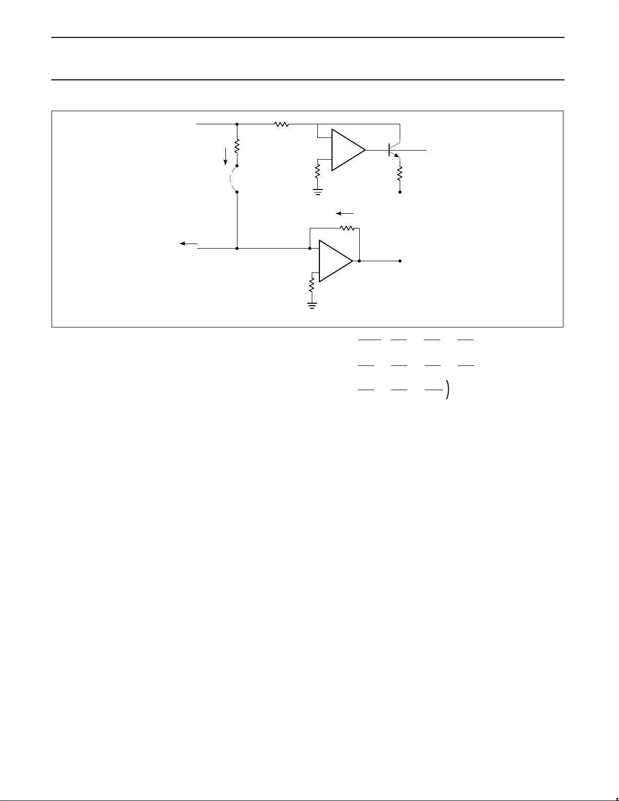
Figure 13. Bipolar Output
DAC
CURRENT
FROM
CURRENT
SWITCHES
OUTPUT
AMP
To R-2R Ladder
DAC
AMP
BIPOLAR
OFFSET (18)
JUMPER FOR
BIPOLAR OPERATION
SUM
NODE (22)
(16)
+
–
–
+
5k
5k
(17)
V
REF
IN
I
D
(ID I
REF
)
V
CC
I
REF
5k
Reference Interface
The NE5020 contains an internal bandgap voltage reference which
is designed to have a very low temperature coefficient and excellent
long-term stability characteristics.
The internal bandgap reference (1.23V) is buffered and amplified to
provide the 5V reference output. Providing a V
REF ADJ
(Pin 14)
allows trimming of the reference output. Utilization of the adjust
circuit shown in Figure 15 performs not only V
REF
adjustment, but
also full-scale output adjust. Notice that the V
REF ADJ
pin is
essentially the sum node of an op amp and is sensitive to excessive
node capacitance. Any capacitance on the node can be minimized
by placing the external resistors as close as possible to the V
REF
ADJ
pin and observing good layout
practices.
The V
REF OUT
node can drive loads greater than the DAC V
REF
input requirements and can be used as an excellent system voltage
reference. However, to minimize load effects on the DAC system
accuracy, it is recommended that a buf fer amplifier be used.
Input Amplifier
The DAC reference amplifier is a high gain internally-compensated
op amp used to convert the input reference voltage to a precision
bias current for the DAC ladder network.
The Block Diagram details the input reference amplifier and current
ladder. The voltage-to-current converter of the DAC amp will
generate a 1mA reference current through QR with a 5V V
REF
. This
current sets the input bias to the ladder network. Data bit 9
(DB9)(Q9), when turned on, will mirror this current and will
contribute 1mA to the output. DB8 (Q8) will contribute 1/2 of that
value or 0.5mA, and so on. These current values act as current
sinks and will add at the sum node to produce a DAC ladder to sum
node function of:
I
OUT
2V
REF
R
REF
DB9
2
DB8
4
DB7
8
DB6
16
DB5
32
DB4
64
DB3
128
DB2
256
DB1
512
DB0
1024
Because of the fixed internal compensation of the reference amp,
the slew rate is limited to typically 0.7V/µs and source impedance at
the V
REF INPUT
greater than 5kΩ should be avoided to maintain
stability.
The –V
REF INPUT
pin is uncommitted to allow utilization of negative
polarity reference voltages. In this mode +V
REF INPUT
is grounded
and the negative reference is tied directly to the –V
REF INPUT
contains a 5kΩ resistor that matches a like resistor in the +V
REF
INPUT
to reduce voltage offset caused by op amp input bias currents.
Output Amplifier and Interface
The NE5020 provides an on-chip output op amp to eliminate the
need for additional external active circuits. Its two-stage design with
feed-forward compensation allows it to slew at 15V/µs and settle to
within ±1/2LSB in 5µs. These times are typical when driving the
rated loads of R
L
≥ 5k and CL 50pF with recommended values of
C
FF
= 1nF and CFB = 30pF. Typical input offset voltages of 5mV
and 50kΩ open-loop gain insure that an accurate current-to-voltage
conversion is performed when using the on-chip R
FB
resistor. R
FB
is matched to R
REF
and R
BIP
to maintain accurate voltage gain over
operating conditions. The diode shown from ground to sum node
prevents the DAC current switches from saturating the op amp
during large signal transitions which would otherwise increase the
settling time.
The output op amp also incorporates output short circuit protection
for both positive and negative excursions. During this fault condition
I
OUT
will limit at ±15mA typical. Recovery from this condition to
rated accuracy will be determined by duration of short-circuit and die
temperature stabilization.
Page 10
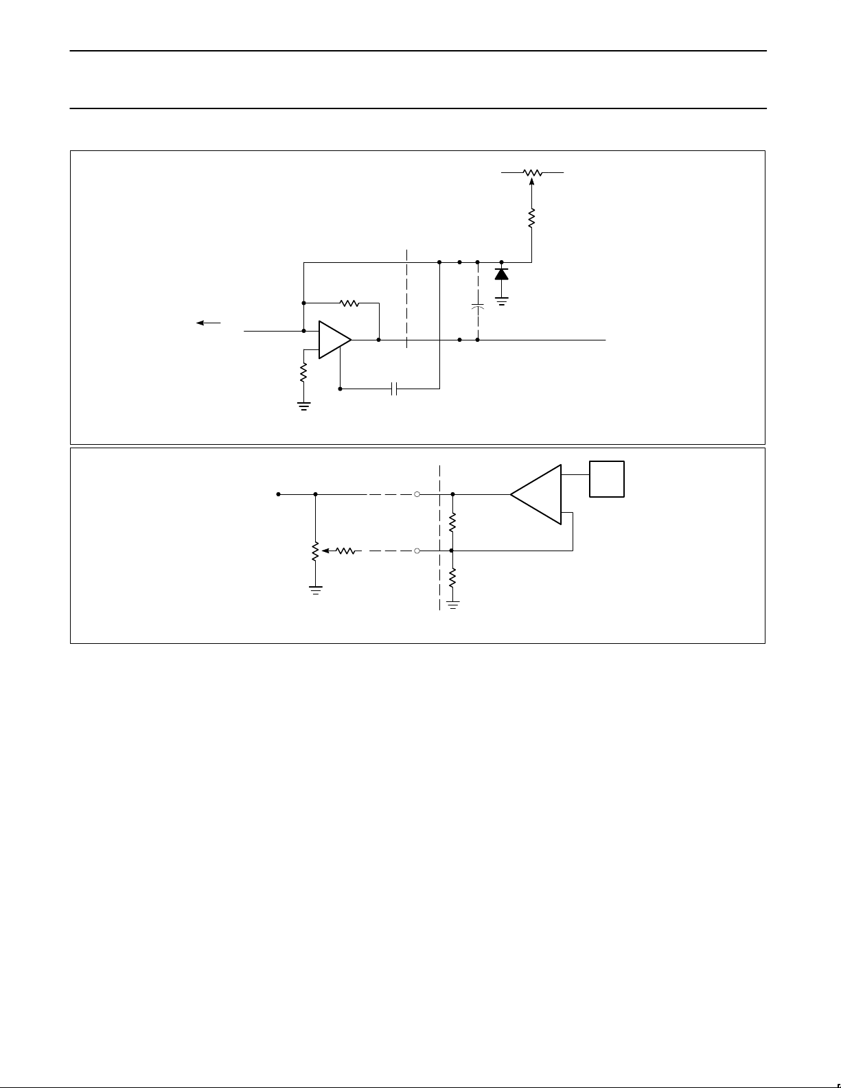
Philips Semiconductors Linear Products Product specification
NE502010-Bit µP-compatible D/A converter
August 31, 1994
766
Figure 14. Zero-Scale Adjustment
DAC
–
+
CURRENT OUTPUT
(24)
5k
AMP
COMP
(23)
5k
SUM
NODE
(22)
(OPTIONAL)
(20)
V
OUT
V
CC
–V
CC
R1 = 20K, 10T POTENTIOMETER
C
FF
C
C
R2 = 1MΩ
Figure 15. Reference Adjust Circuit
+
–
10T POT
5k
(15)
(14)
15k
INT
REF
V
REF
ADJ
V
REF
OUT
V
REF
OUT
R
3
= 10k
R
3
= 80k
Bipolar Output Voltage
The NE5020 includes a thermally matched resistor, R
BIP
, to offset
the output voltage by 5V to obtain –5V to +5V output voltage range
operation. This is accomplished by shorting Pins 18 and 22 (see
Figure 13). This connection produces a current equal to (V
REFIN –
SUM NODE
) ÷ R
BIP
(1mA nominal), which is injected into the sum
node. Since full-scale current out is approximately 2mA
(1.9980mA), (2mA – 1mA)5kΩ = 5V will appear at the output. For
zero DAC output currents, 1mA is still injected into sum node and
V
OUT
= –(5kΩ) (1mA) = –5V. Zero-scale adjust and full-scale adjust
are performed as described below, noting that full-scale voltage is
now approximately +5V. Zero-scale adjust may be used to trim
V
OUT
= 0.00 with the MSB high or V
OUT
= –5.0V with all bits off.
Zero-Scale Adjustment
The method of trimming the small offset error that may exist when all
data bits are low is
shown in Figure 14. The trim is the result of injecting a current from
resistor R
2
that counteracts the error current. Adjusting
potentiometer R
1
until V
OUT
equals 0.000V in the unipolar mode or
–5.000V in the bipolar mode (see bipolar section accomplishes this
trim.
Full-Scale Adjustment
A recommended full-scale adjustment circuit, when using the
internal voltage reference, is shown in Figure 15. Potentiometer R
3
is adjusted until V
OUT
equals 9.99023V. In many applications where
the absolute accuracy of full-scale is of low importance when
compared to the other system accuracy factors this adjustment
circuit is optional.
As resistors R
REF
, RFB, and R
BIP
shown in the Block Diagram are
integrated in close proximity, they match and track in value closely
over wide ambient temperature variations. Typical matching is less
than ±0.3% which implies that typical full-scale (or gain) error is less
than ±0.3% of ideal full-scale value.
 Loading...