

Page 1

INTEGRATED CIRCUITS
NE1619
HECETA 4
Temperature and voltage monitor
Product specification 2000 Jul 13
Page 2

Philips Semiconductors Product specification
NE1619HECETA4 Temperature and voltage monitor
GENERAL DESCRIPTION
The NE1619 is designed for monitoring the temperatures and supply
voltages of microprocessor-based systems by measuring those
parameters and comparing the readings with programmable limits.
The device provides five possible analog inputs, a remote
temperature sensor input and on-board local temperature sensor.
The device also monitors its own power supply and provides digital
inputs for the Pentium/PRO power supply ID code.
The device communicates with the system controller via an SMBus
(System Management bus) by which it can be programmed for
operation and data collection. Readings come from conversions of
the on-board A-to-D converter which cycles through all
measurements in sequence in approximately one second when the
conversion is started. The device includes a number of registers to
store data of the device configuration, status, readings and limits.
Except for the temperature-related data which are in 8-bit digital
2’s complement format, all the data are in 8-bit digital straight format.
FEA TURES
•Monitor local and remote temperatures
•Temperature accuracy of ±2 °C for local, and ±3 °C for remote
channel
•Temperature resolution of 1 °C
•2.8 V to 5.5 V supply range
•Monitor different power supplies: 12 V, 5 V, 3.3 V, 2.5 V, V
•V
accuracy of ±2% of full scale
IN
CCP, VDD
•Differential non-linearity of ±1LSB
•No calibration required
•Programmable temperature and voltage limits for alarms
•Programmable Reset low state pulse output
•SMBus 2-wire serial interface
•Small 16-lead QSOP package
•Compatible with Intel “Heceta 4” specification and reference
designs utilizing it
APPLICATIONS
•System thermal and hardware monitor
•Desktop computers
•Notebook computers
•Industrial controllers
•T elecom equipment
ORDERING INFORMATION
PART NUMBER PACKAGE DRAWING NUMBER
NE1619 16-lead QSOP package SOT519-1
2000 Jul 13 853-2202 24122
2
Page 3

Philips Semiconductors Product specification
NE1619HECETA4 Temperature and voltage monitor
PINNING
Pin Configuration
16SDA
15
14
13
12
11
10
SL01228
A0/RESET
/NTEST_OUT
V
CCPVIN
2.5V
IN
3.3V
IN
5V
IN
12VIN/VID4
D+
D–/NTEST_IN
V
DD
1
2
SCL
3
GND
4
/3.3VSB
5
VID0
6
VID1
7
VID2
89
VID3
Pin Description
PIN # SYMBOL FUNCTION DESCRIPTION
1 SDA Digital I/O. SMBus serial bi-directional data. Open-drain output.
2 SCL Digital Input. SMBus serial clock input.
3 GND Ground. To be connected to system ground.
4 VDD/3.3VSB Power supply. Can be connected to +3.3 V standby power if monitoring in low power states is
5 VID0 Digital Input. For Voltage ID readouts from the processor. This value is read into the VID status
6 VID1 Digital Input. For Voltage ID readouts from the processor. This value is read into the VID status register.
7 VID2 Digital Input. For Voltage ID readouts from the processor. This value is read into the VID status register.
8 VID3 Digital Input. For Voltage ID readouts from the processor. This value is read into the VID status register.
9 D–/NTEST_IN Analog/Digital Input. This pin is connected to the negative terminal of the remote temperature sensor for
10 D+ Analog Input. This pin is connected to the positive terminal of the remote temperature sensor.
11 12VIN/VID4 Analog/Digital Input. Defaults at power-up to analog input for monitoring the +12 V supply. This pin is
12 5V
13 3.3V
14 2.5V
15 V
IN
IN
IN
CCPVIN
16 A0/RESET/NTEST_IN Digital I/O. At power-up, the logic input of this pin defines the LSB bit of the device slave address.
required. This pin also serves as the analog input to monitor the VDD voltage level.
register (LSB bit).
analog input. If this pin is held high at power-up, for digital input, it enables the NAND-TREE test mode.
programmable to be a digital input for voltage ID readouts from the processor. Its state is read into the
VID4 status register.
Analog Input. For monitoring the +5 V supply.
Analog Input. For monitoring the +3.3 V supply.
Analog Input. For monitoring the +2.5 V supply.
Analog Input. For monitoring the processor voltage supply (0 to 3.0 V)
This pin can be configured to give a low pulse reset output of 20ms minimum. This pin also functions
as the output in the NAND–TREE test mode.
2000 Jul 13
3
Page 4

Philips Semiconductors Product specification
NE1619HECETA4 Temperature and voltage monitor
FUNCTIONAL BLOCK DIAGRAM
D+
D-/
NTEST_IN
GND
VDD
V
CCVIN
2.5 VIN
3.3 VIN
5 VIN
12 VIN/
VID4
Local Temp
Sensor
Temp
Mux
A-to-D
Converter
Voltage
Mux
Vin
Attenuators
Switch
Vid4
Register
Control
Logic
Local Temp
RDG Register
Remote Temp
RDG Register
VDD Reading
Register
VCCP Reading
Register
2.5 V Reading
Register
3.3 V Reading
Register
5 V Reading
Register
12 V Reading
Register
SMBus Interface
Configuration
Register
Local Temp
HL Register
Remote Temp
HL Register
VDD HL
Register
VCCP HL
Register
2.5 V HL
Register
3.3 V HL
Register
5 V HL
Register
12 V HL
Register
Command
Pointer Register
Local Temp
LL Register
Remote Temp
LL Register
VDD LL
Register
VCCP LL
Register
2.5 V LL
Register
3.3 V LL
Register
5 V LL
Register
12 V LL
Register
Address Decoder
and Register
Status
Register 1
Status
Register 2
Company #
Register
Step Version
Register
Test
Register
Reset Pulse
Circuit
VID 0-3
Register
NTEST
Circuit
A0/
Reset #/
NTEST_OUT
VID3
VID2
VID1
VID0
2000 Jul 13
SCL
SDA
SL01229
4
Page 5

Philips Semiconductors Product specification
NE1619HECETA4 Temperature and voltage monitor
TYPICAL OPERATING CIRCUIT
Remote Sensor:
V
DD
SMBus
:
CLOCK
DATA
Selectable
A0/RESET/NTEST_OUT
Ground
µP On-Board PNP Transistor
See
Note 1
or Discrete NPN Transistor
0.1 uF
10
10 k 10 k 100 k
4
2
1
9
16
System Power
Supplies
V
CCP
2.5 V
3.3 V
5.0 V
12.0 V
1. May be required in noisy environment, about 1 nF
15
14
13
12
11
NE1619
5
6
7
8
3
Ground
Processor Voltage
ID Code:
VID0
VID1
VID2
VID3
VID4
SL01230
ABSOLUTE MAXIMUM RATINGS
PARAMETER MIN. MAX. UNIT
VDD to GND –0.3 6 V
12VIN to GND –0.3 18 V
5VIN, 3.3VIN, 2.5VIN, V
Other pins to GND –0.3 VDD+0.3 V
Input current at any pin –5 5 mA
Package input current –20 20 mA
Operating temperature range 0 +120 °C
Maximum junction temperature +150 °C
Storage temperature range –65 +150 °C
to GND –0.3 6 V
CCP
2000 Jul 13
5
Page 6

Philips Semiconductors Product specification
NE1619HECETA4 Temperature and voltage monitor
Temp Error vs PC Board Track Resistance
20
15
10
–5
–10
–15
–20
–25
Remote Temp Error(deg. C)
–30
FROM D+ PIN TO GND
5
0
FROM D+ PIN TO VDD
1 10 100
Leakage Resistance (Mohm)
Figure 1. Temp Error vs PC Board Track Resistance
Temp Error vs D+D– Capacitance
0
–1
–2
–3
–4
–5
–6
–7
–8
–9
Temperature Error (deg. C)
–10
1 2.2 3.3 4.7 6.8 10 22 33 47
D+ to D– Capacitance (nF)
SL01245
SL01244
Standby Current vs Supply Voltage
100
80
60
40
20
Stdby Supply Current (uA)
0
0123456
Supply Voltage (V)
Figure 3. Standby Current vs Supply Voltage
Standby Current vs Temperature
50
40
30
20
10
Stdby Supply Current (uA)
0
–50 –25 0 25 50 75 100 125
VDD = 5.0V
VDD= 3.8V
VDD= 3.3V
VDD= 2.8V
Temperatures (deg. C)
SL01243
SL01242
2000 Jul 13
Figure 2. Temp Error vs D+D– Capacitance
Figure 4. Standby Current vs Temperature
6
Page 7
Philips Semiconductors Product specification
NE1619HECETA4 Temperature and voltage monitor
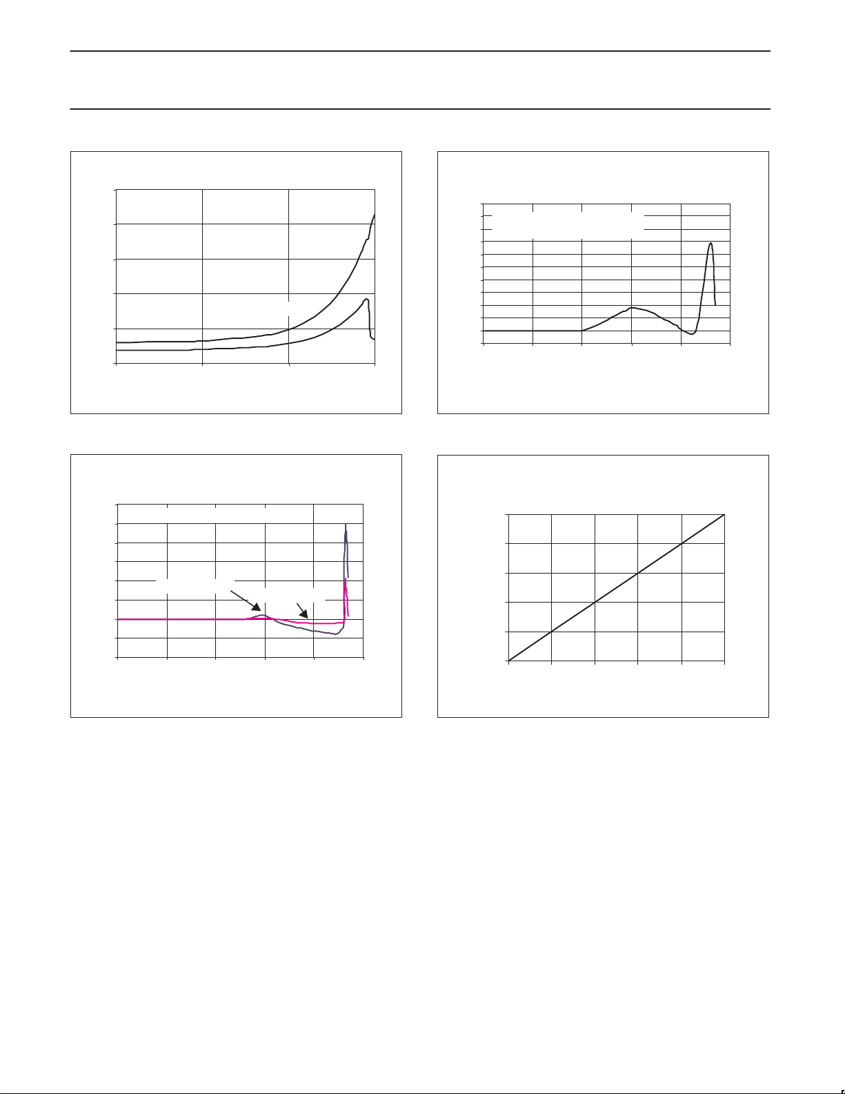
Standby Supply Current vs SCLK Frequency
250
200
150
100
VDD=5V
50
Stdby Supply Current (uA)
0
1K 10K 100K 1000K
SCLK Frequency (Hz)
VDD=3.3V
Figure 5. Standby Current vs SCLK Frequency
Remote Temp Error vs Common–Mode
Noise Frequency
30
NOISE IS AC COUPLED TO D– PINS
25
20
15
10
5
0
–5
Temperature Error (deg. C)
–10
1K 10K 100K 1000K 10000K 100000K
NOISE=100MVPP
Noise Frequency (Hz)
NOISE=50MVPP
Figure 6. Temp Error vs Common Mode Noise
SL01246
SL01241
Remote Temp Error vs Differential–Mode
Noise Frequency
10
9
NOISE=10MVP–P SQ.WAVE
8
APPLIED BETWEEN D+ & D– PINS
7
6
5
4
3
2
1
0
Temperature Error (deg. C)
–1
1K 10K 100K 1000K 10000K 100000K
Noise Frequency (Hz)
SL01240
Figure 7. Temp error vs Different Mode Noise Frequency
Relationship Between Temperature
and Temp Reading
125
100
75
50
25
Temp Reading (Decimal)
0
0 25 50 75 100 125
Temperature (deg. C)
SL01247
Figure 8.
2000 Jul 13
7
Page 8
Philips Semiconductors Product specification
TAIInternal temperature accurac
TAEExternal temperature accurac
ISRemote source current
NE1619HECETA4 Temperature and voltage monitor
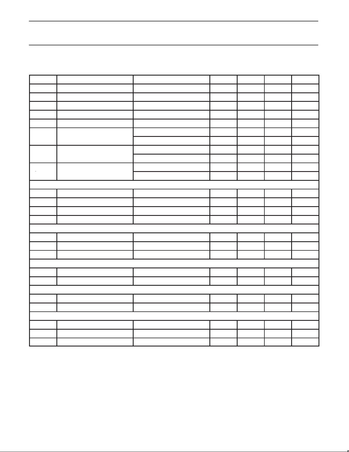
DC ELECTRICAL CHARACTERISTICS
VDD = 3.3 V, T
SYMBOL
V
DD
I
DD
I
DD
t
C
T
R
Voltage-to-Digital converter (12VIN, 5VIN, 3.3VIN, 2.5VIN, V
VUE Unadjusted error ±2.0 %FS
VDNL Dif ferential non-linearity error ±1.0 LSB
VRIN VIN input resistance 100 200 kΩ
VPSS VIN power supply sensitivity ±1.0 %/V
Digital output (SDA, A02)
V
OH
V
OL
I
OH
SMB digital input voltages (SDA, SCL)
V
IH
V
IL
Digital input voltages (A0, VID0–4, NT_IN3)
V
IH
V
IL
Digital input current (all digital inputs)
I
IH
I
IL
C
IN
NOTES:
1. Total monitoring cycle time includes all temperature conversions and all voltage conversions.
2. When A0 is selected as output in NAND-TREE test mode.
3. When D– is selected as input in NAND-TREE test mode.
= 0°C to +120°C unless otherwise specified.
amb
PARAMETER CONDITION MIN. TYP. MAX. UNIT
Supply voltage 2.8 3.3 5.5 V
Supply current Standby mode 100 µA
Supply current Operating mode 250 500 µA
Total monitoring cycle time
1
All conversions 0.25 0.50 sec
T emperature resolution Local and Remote ±1.0 °C
T
= 25°C ±2.0 °C
p
p
y
y
amb
T
= 0°C to +120°C ±3.0 °C
amb
T
= 25°C ±3.0 °C
amb
T
= 0°C to +120°C ±5.0 °C
amb
High level 100 µA
Low level 10 µA
, VDD)
CCP
Output High voltage I
Output Low voltage I
Output High leakage current V
Input High voltage 0.6V
Input Low voltage 0.3V
= –3.0 mA, VDD = 2.8 V 2.4 V
OUT
= 3.0 mA, VDD = 3.8 V 0.4 V
OUT
OUT
= V
DD
0.1 10.0 µA
DD
DD
Input High voltage 2.0 V
Input Low voltage 0.4 V
Input High current VIN = V
DD
–1.0 µA
Input Low current VIN = GND 1.0 µA
Input capacitance 20.0 pF
V
V
2000 Jul 13
8
Page 9
Philips Semiconductors Product specification
NE1619HECETA4 Temperature and voltage monitor
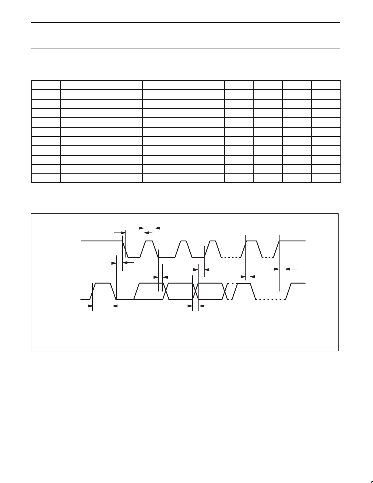
SMBUS INTERFACE AC CHARACTERISTICS
VDD = 3.3 V, T
SYMBOL
t
SCL
t
BUF
t
LOW
t
HIGH
t
SU:STA
t
HD:STA
t
SU:STO
t
SU:DAT
t
HD:DAT
t
F
NOTE:
1. These specifications are guaranteed by design and not tested in production.
= 0°C to +120°C unless otherwise specified.
amb
PARAMETER CONDITION MIN. TYP. MAX. UNIT
SCL clock frequency 400 kHz
SMBus free time 4.7 µs
SCL Low time 4.7 µs
SCL High time 4.0 µs
Start setup time 100 ns
Start hold time 100 ns
Stop setup time 4.0 µs
Data setup time 250 ns
Data hold time 0 ns
Fall time 1.0 µs
TIMING DIAGRAM
SCL
SDA
S: Start Condition
P: Stop Condition
t
HIGH
t
SU:DAT
t
SU:STA
t
F
t
HD:STA
t
BUF
t
LOW
t
HD:DAT
PS PS
t
SU:STO
SL01231
2000 Jul 13
9
Page 10

Philips Semiconductors Product specification
NE1619HECETA4 Temperature and voltage monitor
Table 1. List of registers
NAME COMMAND OR ADDRESS R/W POR STATE DESCRIPTION
CR 40h R/W 0000 1000 Configuration register
SR1 41h Read only 0000 0000 Status register #1
SR2 42h Read only 0000 0000 Status register #2
VID 47h Read only 0000 xxxx VID register, xxxx = VID3–VID0
VID4 49h Read only 1000 000x VID4 register, x = VID4
CID 3Eh Read only TBD Company number
SID 3Fh Read only TBD Stepping version number
TEST 15h R/W N/A Manufacturer test register
2.5VR 20h Read only N/A 2.5VIN reading register
VCCPR 21h Read only N/A V
3.3VR 22h Read only N/A 3.3VIN reading register
5VR 23h Read only N/A 5VIN reading register
12VR 24h Read only N/A 12VIN reading register
VDDR 25h Read only N/A VDD reading register
ETR 26h Read only N/A External or remote temperature reading register
ITR 27h Read only N/A Internal or local temperature reading register
2.5VHL 2Bh R/W 0000 0000 2.5VIN high limit register
2.5VLL 2Ch R/W 0000 0000 2.5VIN low limit register
VCCPHL 2Dh R/W 0000 0000 V
VCCPLL 2Eh R/W 0000 0000 V
3.3VHL 2Fh R/W 0000 0000 3.3VIN high limit register
3.3VLL 30h R/W 0000 0000 3.3VIN low limit register
5VHL 31h R/W 0000 0000 5VIN high limit register
5VLL 32h R/W 0000 0000 5VIN low limit register
12VHL 33h R/W 0000 0000 12VIN high limit register
12VLL 34h R/W 0000 0000 12VIN low limit register
VDDHL 35h R/W 0000 0000 V
VDDLL 36h R/W 0000 0000 V
ETHL 37h R/W 0000 0000 External or remote temperature high limit register
ETLL 38h R/W 0000 0000 External or remote temperature low limit register
ITHL 39h R/W 0000 0000 Internal or local temperature high limit register
ITLL 3Ah R/W 0000 0000 Internal or local temperature low limit register
reading register
CCPVIN
high limit register
CCPVIN
low limit register
CCPVIN
high limit register
DDVIN
low limit register
DDVIN
2000 Jul 13
10
Page 11
Philips Semiconductors Product specification
NE1619HECETA4 Temperature and voltage monitor
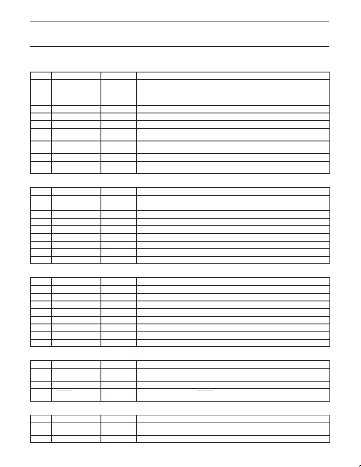
Table 2. Configuration Register (CR, 40h, default = 0000 1000)
BIT NAME R/W DESCRIPTION
0 START R/W Logic 1 enables startup of monitor device, logic 0 places the device in standby mode.
1 Reserved Read Power-up default = 0.
2 Reserved Read Power-up default = 0.
3 Reserved Read Power-up default = 1.
4 RESET R/W Setting this bit generates a minimum 20ms low pulse on the Reset pin, if the reset
5 12VIN/VID4
SELECT
6 Reserved Read Power–up default = 0.
7 Initialization R/W Logic 1 restores power–up default values to the configuration register and the status
R/W Selects whether pin 11 acts as a 12 volt analog input monitoring pin, or as a VID[4] input.
Table 3. Status Register 1 (SR1, 41h, default = 0000 0000)
BIT NAME R/W DESCRIPTION
0 +2.5V_ERROR Read A one indicates 2.5VIN High or Low limit has been exceeded.
Power–up default = 0.
At startup, limit checking functions and scanning begins. Note, all High and Low limits
should be set into the ASIC prior turning on this bit.
function is enabled. Power-up default = 0.
This pin defaults to the 12 volt analog input. Power–up default = 0.
registers. This bit automatically clears itself. Power–up default = 0.
1 VCCP_ERROR Read A one indicates V
2 +3.3V_ERROR Read A one indicates 3.3VIN High or Low limit has been exceeded.
3 +5V_ERROR Read A one indicates 5VIN High or Low limit has been exceeded.
4 Internal Temp Error Read A one indicates internal or local temp High or Low limit has been exceeded.
5 External Temp Error Read A one indicates external or remote temp High or Low limit has been exceeded.
6 Reserved Read
7 Reserved Read
High or Low limit has been exceeded.
CCPVIN
Table 4. Status Register 2 (SR2, 42h, default = 0000 0000)
BIT NAME R/W DESCRIPTION
0 +12V_ERROR Read A one indicates 12VIN High or Low limit has been exceeded.
1 VDD_ERROR Read A one indicates VDD High or Low limit has been exceeded.
2 Reserved Read Undefined.
3 Reserved Read Undefined.
4 Reserved Read Undefined.
5 Reserved Read Undefined.
6 Remote Diode Fault Read A one indicates either a short or open circuited fault on the remote thermal diode inputs.
7 Reserved Read Undefined.
Table 5. VID (VID, 47h, default = 0000 VID[3:0] )
BIT NAME R/W DESCRIPTION
0–3 VID[0:3] Read The VID[0:3] inputs from Pentium/PRO power supplies ID to indicate the operating
4–6 Reserved Read Undefined.
7 RESET ENABLE Read When set to 1, enables the RESET pin output function.
voltage (e.g. 1.5V to 2.9V). Power–up default = VID[0:3].
This bit defaults to 0 at Power–up and enables addressing function.
Table 6. VID4 (VID4, 49h, default = 1000 000VID[4] )
BIT NAME R/W DESCRIPTION
0 VID4 Read VID4 input, if selected, from Pentium/PRO power supplied ID.
1–7 Reserved Read Power-up default = 1000 000
2000 Jul 13
Power–up default = 0 and pin 11 is not selected for VID4.
11
Page 12

Philips Semiconductors Product specification
NE1619HECETA4 Temperature and voltage monitor
FUNCTIONAL DESCRIPTION
SMBus serial interface
The NE1619 can be connected to a compatible 2-wire serial
interface SMBus as a slave device under the control of a master
device or controller, using two device terminals SCL and SDA. The
controller will provide a clock signal to the device SCL pin and
write/read data to/from the device through the SDA pin.
Data of 8-bit digital byte or word are used for communication
between the controller and the device.
Notice that external pull-up resistors, about 10 kΩ, are needed for
the two terminals SCL and SDA.
Slave address
The NE1619 slave address on the SMBus is defined by the
hardware connection applied to the device pin 16. At power-up this
pin is automatically reset to its address sensing function A0. This
logic input will set up the value of the LSB bit of the 7-bit address.
Because A0 is a two-level digital input and the other 6 bits of the
address are predefined to 010110, only two slave addresses can be
used as listed below for the device:
Table 7.
A0 connection (Pin 16) Slave address
GND 0101 100
V
DD
0101101
Because all limit registers are reset to zero, writing limits into the
limits registers should usually be the first action to be performed
after power-on reset.
Initialization
Initialization or software reset of the NE1619 can be initiated by
setting bit 7 of the configuration register. This bit automatically clears
itself after being set. The initialization performs a similar reset function
to power-on reset, except that the reading and limit registers are
not reset.
Starting conversion
The NE1619 monitoring function is started by setting (to 1) the
STAR T bit (bit 0) of the configuration register. The device then
performs a loop of monitoring about every second. In monitoring
function, the device cycles sequentially through all measurements of
temperatures and voltages and also performs the comparisons
between readings and limits accordingly. The inputs are sampled in
this order: Remote diode temperature, Local temperature, V
12V
, 5VIN. 3.3V
IN
Measured values are stored in reading registers and results of limit
comparison are reflected by the state of the flag bits in the status
registers. Reading and status data can be read at any time. Limit
values should be written into limit registers before starting
conversion to avoid false conditions of the status.
Resetting (to 0) the STAR T bit (bit 0) of the configuration register will
stop the monitoring function and put the device into its standby
mode thereby reducing power consumption.
2.5VIN and V
IN,
CCPVIN
.
DDVIN
,
Because the logic is sampled and latched into the device storage
only at power-up, the device pin 16 can be programmed for different
functions while power is on without effecting the address definition.
Registers
The NE1617 contains a number of registers, as listed in Table 1, in
order to store data of the device setup and operation results. The
table indicates the command value and read/write capability of each
register for SMBus communication and also the power-up default
values for some registers. It includes:
– Configuration register to provide control and configuration as well
as initialization the NE1619,
– Status registers to provide the flags resulting from limit
comparisons,
– Reading registers to store results of measurements,
– Limit registers to store programmable limit data,
– ID and test registers.
Data are stored in registers by 8-bit digital byte, either in 2’s
complement format for temperature-related data or in straight format
for others. Writing and reading registers will be done on the SMBus
by a controller using the SMBus protocols that will be described
more in the last section of this functional description. Notice that
attempting to write to a “Read only” register will produce an invalid
result.
Power-on reset
When the power is applied to the NE1619, also called hardware
reset, the registers are reset to their default value, if defined, as
shown in Table 1. The content of registers which have indeterminate
default value such as reading registers will be unknown. The
on-board A-to-D converter is disabled and the monitoring function is
not started. The device enters standby mode and draws a supply
current less than 100µA.
T emperature measurement
The NE1619 contains an on-chip temperature sensor to measure
the local or internal temperature and provides input pins (D– and
D+) to measure the remote or external temperature with the use of a
remote diode-type sensor. The remote sensor should be connected
to the D– and D+ pins properly.
The method of temperature measurement is based on the change of
the diode VBE at two different operating current levels given by:
∆VBE = (KT/q)*LN(N)
where:
K: Boltzmann’s constant
T: absolute temperature in °K
q: charge on the electron
N: ratio of the two currents
LN: natural logarithm
The NE1619 provides two current sources of about 10µA and 100µA
during the measurement of the remote diode VBE and the sensed
voltage between two pins D– and D+ is limited within 0.25V and
0.95V.
The external diode should be selected to meet this current and
voltage requirements. The diode-connected PNP transistor provided
on the Pentium series microprocessor is typically used, or the
discrete diode-connected transistor 2N3904 is recommended.
For temperature measurement, local or remote, the ∆VBE is
converted into digital data by the on-chip sigma-delta A-to-D
converter. The result is stored in the temperature reading register
and is also compared with the limits stored in the temperature limit
registers in order to set the temperature flag bits in the status
register as described in Table 3.
2000 Jul 13
12
Page 13

Philips Semiconductors Product specification
NE1619HECETA4 Temperature and voltage monitor
Temperature data is represented by a digital 8-bit byte or word in
two’s complement format with a resolution of 1°C. Theoretically , the
temperature value can be from –128°C to +127°C but, practically,
the operation range is limited to (0°C, 120°C). Here are some of
temperature values and data:
Table 8.
TEMPERATURE VALUE (°C) TEMPERATURE DATA
+127 0111 1111
+126 0111 1110
+100 01 10 0100
+25 0001 1001
+1 0000 0001
0 0000 0000
–1 1111 1111
–25 1110 0111
–50 1100 1 110
Voltage measurement
The NE1619 provides 5 analog inputs for directly monitoring the
power supplies typically found in a PC, having nominal values of
+2.5 V, +3.3 V, +5.0 V, +12.0 V and V
monitors its own V
which nominal value is 3.3 V. Notice that, at
DD
power-up, the device Pin 11 is defaulted to its 12V
(2.25 V). The device also
CCP
function. These
IN
inputs are internally attenuated by on-chip resistor networks to the
reference levels that are then multiplexed to a 8-bit Delta-Sigma
A-to-D converter for converting into digital data. Each V
input is
IN
overall scaled in such a way that the decimal value of the data for its
nominal voltage value is equal to 192. It means that the overall step
size of the conversion for each V
value. Reading data are stored in the V
also compared with the limits stored in the V
is equal to 1/
IN
IN
192
reading registers and are
limit registers in order
IN
of its nominal
to set the voltage flag bits in the status registers as described in
Tables 3 and 4.
The V
data, different with the temperature data, is represented by
IN
a digital 8-bit byte or word in straight format with a resolution LSB
equal to
This is how to calculate the V
input including V
1
/
of the nominal value, and has any value from 0 to 255.
192
DD
:
error from the VIN reading at any
IN
Resolution in volts: LSB = (VIN nominal in volt)/192
Full scale in volts: FS= 255 * LSB
Reading value in volts: V
Reading error in volts: V
VIN error in % of FS: V
value =
IN
(decimal value of V
error = (VIN value) – (VIN applied)
IN
error % = 100*(VIN error)/FS
IN
reading) * LSB
IN
Applied value < 0 results in a reading of about 0
Applied value > FS results in a reading of about 255
Input safety
Since the power supply voltages will appear directly at VIN pins, a
small external resistor, about 500Ω, should be connected in series
with each pin in order to prevent damaging the power supplies due
to accidental short. These resistors are recommended but not
necessary. No external resistor-divider should be used for the V
IN
pins because of the effect of the internal input resistors, about
140 kΩ at each pin, on the divider accuracy.
Processor Voltage ID (VID)
The NE1619 provides 5 digital pins (VID0–VID4) to read the
processor voltage ID code and store it into the VID registers so that
the code can be read over the SMBus:
VID register: bit 0–bit3 reflect VID0–VID3 respectively
VID4 register: bit 0 reflects VID4
Because the VID4 function of 12V
at power-up (default function of this pin is 12V
/VID4 pin (Pin 11) is not selected
IN
), the process of
IN
selecting this pin must be performed, if VID4 is needed, by setting
(to 1) bit 5 (12V
/VID4 SELECT) of the configuration register.
IN
The default value of bit 0 of the VID4 register is 0.
The VID inputs should not be left floating because they are not
internally biased. If they are not used then they should be connected
to either GND or V
with resistors.
DD
Limit data
High and Low limits for temperatures and voltages should be
programmed into the limit registers using the format as described
above. During monitoring cycle, the measured data is automatically
compared with the limits and flag bits in the status registers are set
accordingly to the results. The assignment of the status bits are
listed in Tables 3 and 4.
Status registers
Results of limits comparisons are reflected by status or flag bits
stored in the status register 1 and 2. If the reading is within the limits
then the corresponding flag bit will be cleared to 0. Otherwise, it will
be set to 1. Status data can be read over the SMBus. Notice that
because the flag bits are automatically updated at every monitoring
cycle, their states only reflect the last measurements.
Diode fault status
The hardware connection at the diode pins (D+ and D–) are also
checked at the measurement of external temperature and the fault
condition is indicated by the flag bit 6 of the status register 2. This bit
is set to 1 if either short or open circuit fault is detected.
RESET output function
The NE1619 Pin 16 can be selected as a reset pulse output. When
this function is selected and the reset pulse is initiated, this pin will
output a single (minimum 20ms) low state pulse.
The reset output function is selected by setting (to 1) the RESET
ENABLE bit (bit 7) of the VID register. Thereafter, the reset pulse is
generated whenever the RESET bit (bit 4) of the configuration
register is programmed to change from 0 to 1.
Because Pin 16 becomes an open-drain output when it is selected
as an output, an external pull-up resistor, about 100 kΩ is needed
for the output operation. This will restrict the address function on
Pin 16 to being high at power-up. Therefore, if multiple NE1619’s
are connected on the same bus, only one can have this function
enabled at one time.
2000 Jul 13
13
Page 14

Philips Semiconductors Product specification
NE1619HECETA4 Temperature and voltage monitor
NAND-tree test
A NAND tree is provided in the NE1619 for Automated Test
Equipment (A TE) board level connectivity testing. The device is
placed into NAND tree test mode by powering up with Pin 9
(D–/NTEST_IN) held high. In this test mode Pin 16
(A0/RESET
input pins become NAND-tree inputs as illustrated in Figure 1.
/NTEST_OUT) becomes the NAND-tree output and all
SDA
SCL
VID0
VID1
Figure 1. NAND-tree circuitry
To perform a NAND tree test all pins should be initially driven low.
Then one-by-one toggle them high (and keep them high), starting
with the input closest to the output, cycling toward the farthest, the
NAND tree output will toggle with each input change.
VID2
VID3
VID4
NTEST_OUT
SL01232
Table 9. NAND-tree test vectors
VECTOR # SDA SCL VID0 VID1 VID2 VID3 VID4 NTEST_OUT
1 L L L L L L L H
2 L L L L L L H L
3 L L L L L H H H
4 L L L L H H H L
5 L L L H H H H H
6 L L H H H H H L
7 L H H H H H H H
8 H H H H H H H L
2000 Jul 13
14
Page 15
Philips Semiconductors Product specification
NE1619HECETA4 Temperature and voltage monitor
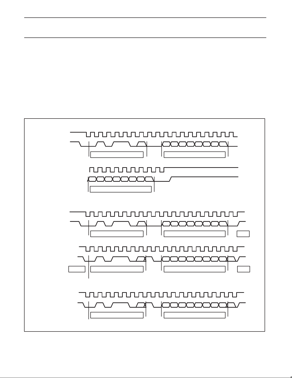
SMBus interface protocol
The NE1619 can communicate over a compatible 2-wire serial
interface SMBus using the two device pins SCL and SDA. The
device employs three standard SMBus protocols: Write Byte, Read
Byte and Receive byte.
Data formats of those protocols are shown below with following notices:
•The SMBus controller initiates data transfer by establishing a start
condition (S) and terminates data transfer by generating a stop
condition (P).
•Data is sent over the serial bus in sequence of 9 clock pulses for
each 8-bit data byte followed by 1-bit status of the device
acknowledgement (A).
Write Byte Format:
SCL
SDA
SCL (continued)
SDA (continued)
123456789123456789
010110a0
SWA A
DEVICE ADDRESS
123456789
D7 D6 D5 D4 D3 D2 D1 D0
DATA TO BE WRITTEN TO REGISTER
•The 7-bit slave address is replaced by the selected address of the
device.
•The command byte is replaced by the selected command of the
device register.
•The receive byte format is used for quickly transfer data from a
reading register which was previously selected by a read.
•During the transition between start and stop conditions, data must
be stable and valid when the SCL is high.
(TO NEXT)
D7 D6 D5 D4 D3 D2 D1 D0
DEVICE REGISTER COMMAND
AP
(TO NEXT)
Read Byte Format:
SCL
SDA
SCL (continued)
SDA (continued)
Receive Byte Format:
SCL
SDA
123456789123456789
(TO NEXT)
010110a0
SWA AP
DEVICE ADDRESS
123456789123456789
0 1 0 1 1 0 a0 D7 D6 D5 D4 D3 D2 D1 D0
SRA NAP
RESTART DEVICE ADDRESS
123456789123456789
010110a0 D7D6D5D4D3D2D1D0
SRA NAP
DEVICE ADDRESS
(end)
D7 D6 D5 D4 D3 D2 D1 D0
DATA REGISTER COMMAND
DATA FROM DEVICE REGISTER
DATA FROM DEVICE REGISTER
(TO NEXT)
STOP
STOP
SL01233
Figure 2. NE1619 SMBus interface protocols
2000 Jul 13
15
Page 16

Philips Semiconductors Product specification
NE1619HECETA4 Temperature and voltage monitor
NOTES
2000 Jul 13
16
Page 17
Philips Semiconductors Product specification
NE1619HECETA4 Temperature and voltage monitor
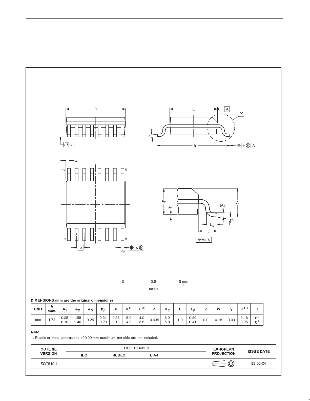
SSOP16: plastic shrink small outline package; 16 leads; body width 3.9 mm;
lead pitch 0.635 mm SOT519-1
2000 Jul 13
17
Page 18

Philips Semiconductors Product specification
NE1619HECETA4 Temperature and voltage monitor
Data sheet status
Data sheet
status
Objective
specification
Preliminary
specification
Product
specification
Product
status
Development
Qualification
Production
Definition
This data sheet contains the design target or goal specifications for product development.
Specification may change in any manner without notice.
This data sheet contains preliminary data, and supplementary data will be published at a later date.
Philips Semiconductors reserves the right to make changes at any time without notice in order to
improve design and supply the best possible product.
This data sheet contains final specifications. Philips Semiconductors reserves the right to make
changes at any time without notice in order to improve design and supply the best possible product.
[1]
[1] Please consult the most recently issued datasheet before initiating or completing a design.
Definitions
Short-form specification — The data in a short-form specification is extracted from a full data sheet with the same type number and title. For
detailed information see the relevant data sheet or data handbook.
Limiting values definition — Limiting values given are in accordance with the Absolute Maximum Rating System (IEC 134). Stress above one
or more of the limiting values may cause permanent damage to the device. These are stress ratings only and operation of the device at these or
at any other conditions above those given in the Characteristics sections of the specification is not implied. Exposure to limiting values for extended
periods may affect device reliability.
Application information — Applications that are described herein for any of these products are for illustrative purposes only. Philips
Semiconductors make no representation or warranty that such applications will be suitable for the specified use without further testing or
modification.
Disclaimers
Life support — These products are not designed for use in life support appliances, devices or systems where malfunction of these products can
reasonably be expected to result in personal injury . Philips Semiconductors customers using or selling these products for use in such applications
do so at their own risk and agree to fully indemnify Philips Semiconductors for any damages resulting from such application.
Right to make changes — Philips Semiconductors reserves the right to make changes, without notice, in the products, including circuits, standard
cells, and/or software, described or contained herein in order to improve design and/or performance. Philips Semiconductors assumes no
responsibility or liability for the use of any of these products, conveys no license or title under any patent, copyright, or mask work right to these
products, and makes no representations or warranties that these products are free from patent, copyright, or mask work right infringement, unless
otherwise specified.
Philips Semiconductors
811 East Arques Avenue
P.O. Box 3409
Sunnyvale, California 94088–3409
Telephone 800-234-7381
Copyright Philips Electronics North America Corporation 2000
All rights reserved. Printed in U.S.A.
Date of release: 07-00
Document order number: 9397 750 07323
2000 Jul 13
18
 Loading...