

Page 1
DATA BULLETIN
VSR CODEC WITH
MX812
Features and Applications
• Half-Duplex Voice Storage and Retrieval
• Serial Bus
• On-Chip DRAM Controller
• Up To 2 Minutes of High-Quality
Recorded Audio
• Answering Functions and VoiceNotepad
• Low-Power 5-Volt CMOS
µµ
µProcessor Control
µµ
DRAM CONTROL
PRELIMINARY INFORMATION
• Selectable Sample Rates and “Memory
Size”
MX812DW MX812J
28-pin SOIC 28-pin CDIP
CLOCK
AUDIO OUT
V
BIAS
AUDIO IN
E
BIAS
V
DD
V
SS
CHIP SELECT
SERIAL CLOCK
COMMAND DAT A
REPLY DATA
IRQ
CLOCK
GENERA TOR
DEMOD
CV S D
CODEC
MOD
POWER METER
STATUS REGISTER
SERIAL
C-BUS
INTERFACE
and
LOGIC
STORE/PLA Y/WAIT COMMAND BUFFER
MODE REGISTER
DRAM
CONTROL
WE
CAS
RAS1
A10/R2
A9
A8
A7
A6
A5
A4
A3
A2
A1
A0
D
DGND
EXTERNAL
DRAM
1 or 2 x
1Mbit
DRAM
Chips
or
1 x
4Mbit
DRAM
Chip
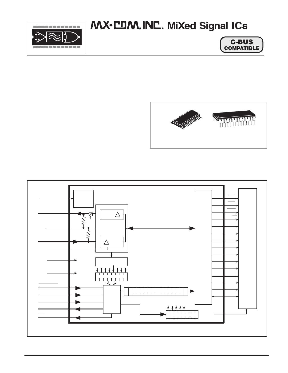
Figure 1 - MX812 Voice Store and Retrieve Codec
© 1997 MX•COM Inc. www.mxcom.com Tele: 800 638-5577 910 744-5050 Fax: 910 744-5054 Doc. # 20480076.003
4800 Bethania Station Road, Winston-Salem, NC 27105-1201 USA All trademarks and service marks are held by their respective companies.
Page 2

VSR CODEC with DRAM CONTROL 2 MX812 PRELIMINARY INFORMATION
DESCRIPTION
The MX812 is a half-duplex VSR Codec, which
when connected to an audio processing microcircuit
(such as the MX816, 826 or 836), provides the storage
and recovery of speechband audio in attached Dynamic
RAM. The addition of this device will enhance the
communications system by providing cellular radios
with Answering Functions, “Message-Notepad” and
general announcement cababilities.
The MX812 will enable:
• Storage of a speech message for transmission
(replay) at a later time.
• Storage of a received speech message when the
operator is not attending.
• The storage and subsequent replay of speech.
All VSR operating functions are controlled by a
simple serial µProcessor interface which may operate
from the radio’s own µProcessor/Controller.
Input audio from the “Store” output of the audio
processor is digitized by delta modulation and stored
via the DRAM controller, in attached memory.
Audio for replay is recovered from the assigned
memory locations and after demodulation made
available for supply to the “Play” input of the audio
processor. For use with other audio systems, the input/
output audio can be connected to relevant points in
circuit.
The MX812 has no on-chip input or output audio
filtering; this capability must therefore be provided by
the host system. Sampling rates and memory capacity
are selectable to 32kb/s or 63kb/s and 1 x 4Mbit or 2 x
1Mbit respectively, which when used in conjunction
allow control of audio-quality and storage-time.
This low-power CMOS device is available 28-pin
plastic SOIC and 28-pin Cerdip packages.
Pin Function
1 CAS: This output should be connected to the “Column Address Strobe” input pin(s) of all DRAM
devices installed.
2 WE: This output should be connected to the “Write Enable” input pin(s) of all DRAM devices installed.
3D: Digital (speech) data into and out of the VSR Codec. This pin should be connected to the “Data
In” and “Data Out” pins (“D” and “Q”) of DRAM devices.
4 Xtal: The nominal 4.0MHz clock input to the VSR Codec. The signal applied to this device may be
derived from the attached Audio Processor on-chip Xtal Oscillator circuits (see Figures 2 and 3).
Note that the VSR Codec will be able to function and maintain correct DRAM refresh, with Xtal input
frequencies down to 2.0MHz. Compand and Local Decoder time constants will change accordingly
and minimum “C-BUS” timings (Figures 6 and 7) would have to be increased pro-rata.
5 Interrupt Request (IRQ): This Interrupt Request output from the MX812 is ‘wire-OR able’ allowing
the Interrupt Outputs of other peripherals to be commoned and connected to the Interrupt input of the
µProcessor (see the C-BUS Interface and System Applications document). This input has a lowimpedance pulldown to VSS when active, and a high-impedance when inactive.
6 Serial Clock: The C-BUS serial clock input. This clock produced by the µController, is used for
transfer timing of commands and data to and from the VSR Codec. See Timing Diagrams.
7 Command Data: The C-BUS serial (command) data input from the µController. Data is loaded to
this device in 8-bit bytes MSB (B7) first and LSB (B0) last, synchronized to the Serial Clock.
8 Chip Select (CS): The C-BUS data transfer control function. This input is provided by the
µController. Transfer sequences are initiated, completed or aborted by this signal. See Timing
Diagrams.
9 Reply Data: The C-BUS serial data output to the µController. The transmission of reply bytes is
synchronized to the Serial Clock under the control of the Chip Select input. This is a 3-state output
which is held at a high-impedance when not sending data to the µController.
10 V
: The output of the internal analog circuitry bias line, held internally at VDD/2. This pin should be
BIAS
decoupled to VSS by capacitor C2 (see Figure 2).
© 1997 MX•COM Inc. www.mxcom.com Tele: 800 638-5577 910 744-5050 Fax: 910 744-5054 Doc. # 20480076.003
4800 Bethania Station Road, Winston-Salem, NC 27105-1201 USA All trademarks and service marks are held by their respective companies.
Page 3
VSR CODEC with DRAM CONTROL 3 MX812 PRELIMINARY INFORMATION
Pin Function
11 Audio Out: The analog output to the Audio Processor “Play” input when the VSR Codec is
configured as a Decoder. When configured as an active Decoder but with no Play Page commands
(62H) active, the VSR Codec will play-out an idle pattern of “101010........10s”. When not configured as
a Decoder, or Powersaved (Mode Register), this output will be held at V
resistor. The output at this pin is unfiltered; an external speechband filter – such as that included on
the MX816/826/836 Audio Processors – will be required. Since this output is centered around VDD/2 a
coupling capacitor is required.
via an internal 500kΩ
BIAS
12 E
: The Encoder d.c. internal balancing circuitry line. This pin should be decoupled to VSS by
BIAS
capacitor C4 (see Figure 2). Note that in the ‘Encode’ mode (Mode Register DE and PS both “0”) the
Codec drives this pin to approximately VDD/2 through a very high impedance; it can take more than
one second for the E
voltage to stabilize when power is first applied to this device. A faster start-up
BIAS
can be achieved by setting Bit DE or PS to “1” for 250mS (approx) during power-up. This will cause
the E
pin to be connected to V
BIAS
through a resistance of approximately 100kΩ.
BIAS
13 Audio In: The analog input to the VSR Codec in the Encode mode. When not configured as an
Encoder, or Powersaved (Mode Register), this input will be held at V
via an internal 500kΩ resistor.
BIAS
This pin should be coupled via a capacitor, see Figure 2. As this input does not contain an internal
audio filter, the audio to this pin should be limited to a 3400Hz “speechband” by an external audio filter
– such as included in the MX816/826/836 Audio Processors.
14 VSS: The “analog” ground connection. See D
description.
GND
15 A0:
16 A1:
17 A2:
18 A3:
19 A4:
20 A5:
DRAM address line outputs from the MX812.
These pins should be connected to the corresponding address
inputs of the associated DRAM.
21 A6:
22 A7:
23 A8:
24 A9:
25 A10/R2: A dual function output pin selected by the memory size (MS) bit (Mode Register),
as detailed in the table below:
MS bit DRAMs Connected To This Output
“0” 1Mbits' DRAM No 2 RAS RAS2
“1” 4Mbit DRAM A10 A10 Signal
26 RAS: An output from the VSR Codec which should be connected to the “Row Address Strobe” pin of
the 4Mbit DRAM or the first 1Mbit DRAM, see Figure 4, Example DRAM connections.
27 D
: The digital signal ground connection to the VSR Codec. Both D
GND
and VSS pins should be
GND
connected to the negative side of the d.c. power supply. However, a printed circuit board should be
laid out so that D
is connected as closely as possible to the DRAM section ground pins.
GND
28 VDD: Positive supply rail. A single, stable +5-volt supply is required. Levels and voltages within the
VSR Codec are dependent upon this supply. This pin should be decoupled to VSS via capacitor C5,
located close to the MX812 pins.
© 1997 MX•COM Inc. www.mxcom.com Tele: 800 638-5577 910 744-5050 Fax: 910 744-5054 Doc. # 20480076.003
4800 Bethania Station Road, Winston-Salem, NC 27105-1201 USA All trademarks and service marks are held by their respective companies.
Page 4
VSR CODEC with DRAM CONTROL 4 MX812 PRELIMINARY INFORMATION
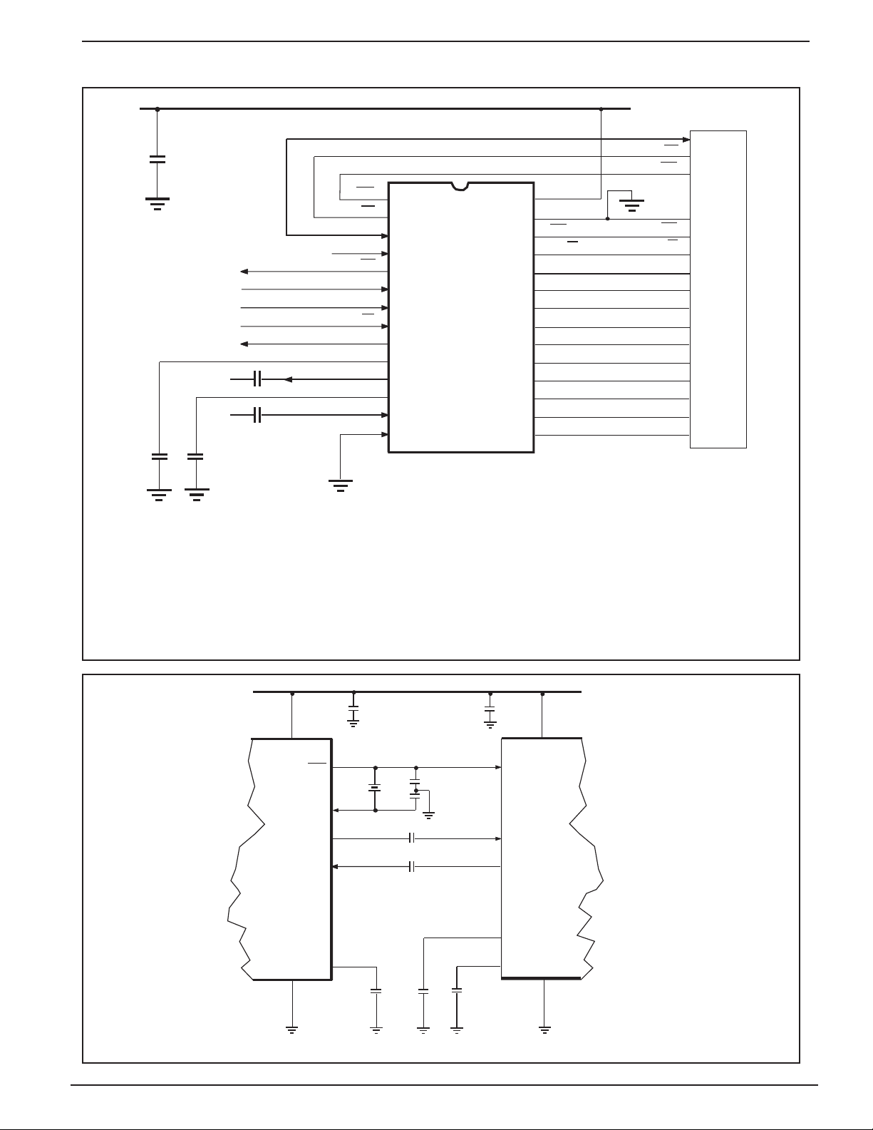
Application Information
V
DD
C
5
V
CAS
1
WE
2
D
SS
IRQ
CS
3
4
5
6
7
8
9
10
11
12
13
14
MX812J
XT AL
SERIAL CLOCK
COMMAND DATA
REPLY DATA
V
C
1
C
3
C
2
C
4
BIAS
AUDIO OUT
E
BIAS
AUDIO IN
V
28
27
26
25
24
23
22
21
20
19
18
17
16
15
DD
D
GND
RAS
A10/R2
A9
A8
A7
A6
A5
A4
A3
A2
A1
A0
WE
CAS
D
RAS
A10/R2
GND
A9
A8
A7
A6
A5
A4
A3
A2
A1
A0
D
D
R
A
M
Component Value
C
1
C
2
C
3
C
4
Tolerance: Capacitors = -50/+100%
Figure 2 - Recommended External Components
+ 5.0V
V
DD
XTAL
XTAL/CLOCK
STORE
Cellular
Audio
PLAY
Processor
eg. MX8n6
Dependent upon the input
impedance of the driven stage
1.0µF
0.1µF
1.0µF non-electrolytic
V
CC
XTAL
AUDIO IN
AUDIO OUT
MX812
E
BIAS
V
BIAS
V
SS
V
BIAS
V
SS
Figure 3 - Interfacing to an Audio Processor
© 1997 MX•COM Inc. www.mxcom.com Tele: 800 638-5577 910 744-5050 Fax: 910 744-5054 Doc. # 20480076.003
4800 Bethania Station Road, Winston-Salem, NC 27105-1201 USA All trademarks and service marks are held by their respective companies.
Page 5

VSR CODEC with DRAM CONTROL 5 MX812 PRELIMINARY INFORMATION
Application Information ......
+ 5.0V + 5.0V
V
DD
MX812
D
GND
CAS
RAS1
A10/R2
A9
A8
A7
A6
A5
A4
A3
A2
A1
A0
D
WWE
CAS
RAS
A10
A9
A8
A7
A6
A5
A4
A3
A2
A1
A0
Q
D
V
CC
4Mbit.
DRAM
V
SS
V
DD
MX812
D
GND
WE
WE
CAS
RAS1
A10/R2
A9
A8
A7
A6
A5
A4
A3
A2
A1
A0
V
CC
W
CAS
RAS
A9
A8
A7
1Mbit.
A6
DRAM.
A5
No.1
A4
A3
A2
A1
A0
Q
D
D
V
SS
Figure 4 - Example DRAM Connections
Choice of DRAM Devices
DRAM devices chosen should be standard 1,048,576 x 1 or 4,194,304 x 1 Dynamic Random Access
memories, with ‘CAS before RAS’ refresh, and a Row Address access time of 200 nano-seconds or less.
BANK
SELECT
INPUTS
A
B
'HC04
'HC00
W
CAS
RAS
A9
A8
A7
A6
A5
A4
A3
A2
A1
A0
Q
D
V
CC
1Mbit.
DRAM.
No.2
V
SS
MX812
WE
CAS
RAS1
A10/R2
A9
A8
A7
A6
A5
A4
A3
A2
A1
A0
W
CAS
RAS
A10
A9
A8
A7
A6
A5
A4
A3
A2
A1
A0
4Mbit
DRAM
No. 1
Q
D
D
Figure 5 - Use of External Elements to Drive Two 4-MBit DRAM Chips
Driving Two 4-MBit DRAM Sections
By adding external logic circuitry, the MX812 can be configured
to drive two 4-MBit DRAM sections. This will have the effect of
doubling the available storage time. i.e. 4 minutes at 32kbps.
With reference to the circuitry shown in Figure 5:
With the Mode Register MS Bit set to “0” the MX812 treats the
DRAM sections as two 1-Mbit devices. The external logic makes
each 4-MBit DRAM appear as four 1-MBit banks selected by the
Bank Select lines ‘A’ and ‘B.’
Bank Select DRAM No 1 DRAM No 2
Inputs Pages Pages
AB0 – 1023 1024 – 2047
00
10
01
11
W
CAS
RAS
A10
A9
A8
A7
A6
A5
A4
A3
A2
A1
A0
Q
D
4Mbit
DRAM
No. 2
© 1997 MX•COM Inc. www.mxcom.com Tele: 800 638-5577 910 744-5050 Fax: 910 744-5054 Doc. # 20480076.003
4800 Bethania Station Road, Winston-Salem, NC 27105-1201 USA All trademarks and service marks are held by their respective companies.
Page 6

VSR CODEC with DRAM CONTROL 6 MX812 PRELIMINARY INFORMATION
The Controlling System: C-BUS Hardware Interface
C-BUS is MX-COM's proprietary standard for the transmission of commands and data between a µController and MX-COM's
New Generation integrated circuits. C-BUS is designed for a low IC pin-count, flexibility in handling variable amounts of data,
and simplicity of system design and µController software.
It may be used with any µController, and can, if desired, take advantage of the hardware serial I/O functions built into many
types of µController. Because of this flexibility and because the BUS data-rate is determined solely by the µ Controller, the
system designer can choose a µController appropriate to the overall system processing requirements.
Control of the functions and levels within the MX812 VSR Codec is by a group of Address/Commands and appended data
instructions from the system µ Controller to set/adjust the functions and elements of the MX812. The use of these instructions
is detailed in the following paragraphs and tables.
Command Address/Command (A/C) Byte + Data
Assignment Hex. Binary Byte/s
MSB LSB
General Reset 01 0 0 0 00001
Write to Mode Register 60 0 1 1 00000 + 1 byte Instruction to Mode Register
Read Status Register 61 0 1 1 00001 + 1 byte Reply from Status Register
Store/Play Page 62 0 1 1 00010 + 2 bytes Command
Wait 63 0 1 1 00011
Table 1 – C-BUS Address/Commands
“Write to Mode Register”
– A/C 60H, followed by 1 byte of Command Data.
Interrupt Output – IE
Controls the MX812 IRQ output driver.
Sampling Rates – SR
The CVSD Codec sampling rates. Accurate rates depend
upon the applied Xtal/clock frequency (see Table 5).
Memory Size – MS
The MX812 can operate with 1 x 1Mbit, 2 x 1Mbit or
1 x 4Mbit of DRAM (see Figure 4).
Powersave – PS
Powersaves the CVSD Codec only. Logic functions and
DRAM refresh are maintained.
Decode/Encode – DE
The Codec and DRAM operational mode.“
“Play” or “Store”
Interrupts
The MX812's Interrupt Output is driven by the Status Bit 7 (IF)
when the Mode Register Bit7 (IE) is set to a “1.”
The IF bit and the Interrupt Output (If enabled) are set when
the Store/Play/Wait command Buffer is emptied (MT bit) by
transferring from the buffer to the DRAM control circuits.
and/or
The IF bit and the Interrupt Output (if enabled) are set when
a Store, Play or Wait command has finished and the Command
Buffer is empty.
The notes below illustrate the IRQ pin conditions:
IF Bit IE Bit IRQ
“0” cleared “0” disable High Z
“0” cleared “1” enable High Z
“1” Interrupt “0” disable High Z
“1” Interrupt “1” enable V
(logic “0”)
SS
Setting
MSB
7
1
0
6
1
0
5
1
0
4
1
0
3
1
0
210
000
Mode Bits
Transmitted to 812 First
Interrupt Output
Enable
Disable
Sampling Rate
63kb/s
32kb/s
Memory (DRAM) Size
Single 4Mbit
1 or 2 x 1Mbit
Powersave
CVSD Codec Powersaved
CVSD Codec Powered
Decode/Encode
Decode – Play Mode
Encode – Store Mode
Not Used
Set to ‘zeros’
Table 2 - Control Register
“General Reset” – A/C 01
Upon Power-Up the “bits” in the MX812 registers will be
random (either “0” or “1”). A General Reset Command (01
will be required to “reset” all microcircuits on the C-BUS, and
has the following effect upon the MX812.
Clear all Mode Register bits to “0”
Status Register Bit 7 (IF) to “0”
Bits 5 and 6 (MT and I) to “1”
Halt any current Store, Play or Wait execution
Clear the Store/Play/Wait Command Buffer
H
H
)
© 1997 MX•COM Inc. www.mxcom.com Tele: 800 638-5577 910 744-5050 Fax: 910 744-5054 Doc. # 20480076.003
4800 Bethania Station Road, Winston-Salem, NC 27105-1201 USA All trademarks and service marks are held by their respective companies.
Page 7

VSR CODEC with DRAM CONTROL 7 MX812 PRELIMINARY INFORMATION
The Controlling System ......
“Read Status Register” – A/C 61
Reading
MSB
7
1
0
6
1
0
5
1
0
43210
Table 3 Status Register
Status Bits
Received from 812 First
Interrupt Condition (Flag)
Bit 6 or 5 set to a “1”
Cleared condition
Command Buffer
Buffer Empty
Cleared condition
Device Condition
Storing, Playing or Waiting
Input Power Level
Store/Play/Wait Command Buffer
A buffer used to accept and hold the latest Store, Play or
Wait command received over the C-BUS while the MX812 is
executing the previous command. The Status Register, bit 6,
indicates the condition of this buffer.
When a command is received it is first loaded into this
buffer. If the MX812 is already executing a previously loaded
Store, Play or Wait command the new command will be stored
temporarily in the Command Buffer, from where it will be taken
on completion of the previous command.
, followed by 1 byte of Reply Data.
H
Interrupt Condition (Flag) – IF
Set to a logic “1” whenever Bit 6 or Bit 5 goes from “0” to
“1” (unless the transition is caused by a General Reset
command 01
while Interrupts are disabled.
Cleared to a logic “0” by a General Reset command or
immediately following a read of the Status Register.
Command Buffer Status – MT
Set to a logic “1” when the Command Buffer is empty or
by a General Reset command.
Cleared to a logic “0” by loading a new Store, Play, Wait
Idle
commands.
Device Condition – I
Set to a logic “1” when NO Store, Play or Wait command
is being executed or by a General Reset command.
Set to a logic “0” while a Store, Play or Wait command is
being executed.
Encode Input Power Level – POWER
Available in the Encode mode, a 5-bit representation of
the analog signal input level, updated at the end of every
Store or Wait command.
This permits the MX812 to perform a continuous sequence
of Store, Play or Wait commands, without gaps and without
requiring an unduly fast response from the mController.
Note that this Command Buffer can only hold one Store,
Play or Wait instruction, each new command received into this
buffer will overwrite any previously loaded contents.
To Store or Play a sequence of pages the relevant commands
should be loaded with sequential page numbers while observing
the Status Register – Bit 6.
). This indication allows monitoring by ‘poll’
H
“Store/Play Page” – A/C 62
For the purposes of storage and replay, the attatched
DRAM is divided into ‘data-pages’ of 1024 bits (1kbit).
One Store/Play command (loaded MSB first) will instruct
the MX812 to store or play (depending upon the setting of the
Mode Register, Bit-3) to or from 1 x 1024 “page” of DRAM.
The Store/Play/Wait command buffer will allow continuity of
, followed by 2 bytes of Command Data.
H
operation.
The particular page selected is identified by the 12 lowest
bits of the 2 x Store/Play bytes as shown below.
If a Store command is loaded and executed whilst the
Codec is “Powersaved” in the Encode mode, the selected
DRAM page will be filled with an idle pattern (“101010.....”).
Bit Number
MSB – Loaded to MX812 First Loaded Last – LSB
Bit151413121110987 6543210Bit
11
10
9
8
7
6
5
4
3
2
Value x x x x 2
2
2
2
2
2
2
2
2
2
1
2
20 Value
Page “0” “0” “0 ” “0” ––––––––––––––––––––––– DRAM Page Number ––––––––––––––––––––––– Page
DRAM Size Valid Page Nos Bit Nos
4Mbit 0 – 4095 0 – 11
1 + 1Mbit 0 – 2047 0 – 10
1Mbit 0 – 1023 0 – 9
“Wait” – A/C 63
Causes the MX812 to wait for 1024 bit periods (approximately
16 or 32ms).
If the Codec is set to the Encode mode, a new “Power”
, –– Wait for 1024 bit periods
H
reading that is relevant to the input audio level, will be loaded
into the Status Register at the end of the Wait period.
If the Codec is set to the Decode mode it will ‘Play’ a perfect
idle pattern (“101010..........”) during the Wait period.
© 1997 MX•COM Inc. www.mxcom.com Tele: 800 638-5577 910 744-5050 Fax: 910 744-5054 Doc. # 20480076.003
4800 Bethania Station Road, Winston-Salem, NC 27105-1201 USA All trademarks and service marks are held by their respective companies.
Page 8

VSR CODEC with DRAM CONTROL 8 MX812 PRELIMINARY INFORMATION
Control Timing Information
Figure 6 shows the timing parameters for two-way communication between the µController and Cellular peripherals on the
“C-BUS.” Figure 7 shows the timing relationships between the Serial Clock and Data.
t
CHIP SELECT
t
CSE
SERIAL CLOCK
COMMAND DATA
76543210 76543210
MSB LSB
ADDRESS/COMMAND
REPL Y DATA
Logic level is not important
BYTE
t
NXT
t
CK
FIRST DATA BYTE LAST DATA BYTE
76543210
MSB
FIRST REPLY DATA BYTE LAST REPLY DATA BYTE
LSB
t
NXT
76543210
76543210
CSOFF
t
CSH
t
HIZ
Figure 6 - Control Timing Information
t
t
CDS
CK
t
CL
t
CH
t
70% VDD
30% VDD
CDH
Figure 7 - Control Timing Relationships
I bit (idle)
Device Condition
MT bit Command
Buffer Status
IF bit (Flag)
COMMAND DATA
(from C)
SERIAL CLOCK
(from C)
REPLY DATA
(to C)
t
RDS
t
RDH
Interrupt
(IRQ) Output
New 'Store, Play orWait'
Command from C-BUS
C1 C2
C3
Read Status Register
** ** **
C2
C3
Command Executing
** The value read from the Status Register at these times will include a valid 'Power' reading if the Codec is set to the E ncode mode.
C1
Figure 8 - Typical Command Sequences
© 1997 MX•COM Inc. www.mxcom.com Tele: 800 638-5577 910 744-5050 Fax: 910 744-5054 Doc. # 20480076.003
4800 Bethania Station Road, Winston-Salem, NC 27105-1201 USA All trademarks and service marks are held by their respective companies.
Page 9

VSR CODEC with DRAM CONTROL 9 MX812 PRELIMINARY INFORMATION
Control Timing Information ......
Timing Specification – Figures 6 and 7
Characteristics See Note Min. Typ. Max. Unit
t
CSE
t
CSH
t
HIZ
t
CSOFF
t
CK
t
NXT
t
CH
t
CL
t
CDS
t
CDH
t
RDS
t
RDH
“CS-Enable to Clock-High” 2.0 – – µs
Last “Clock-High to CS-High” 4.0 – – µs
“CS-High to Reply Output Tri-state” – – 2.0 µs
“CS-High” Time between transactions 2.0 – – µs
“Clock-Cycle” Time 2.0 – – µs
“Inter-Byte” Time 4.0 – – µs
“Serial Clock-High” Period 500 – – ns
“Serial Clock-Low” Period 500 – – ns
“Command Data Set-Up” Time 250 – – ns
“Command Data Hold” Time 0 – – ns
“Reply Data Set-Up” Time 250 – – ns
“Repy Data Hold” Time 50.0 – – ns
Address Line Decoding
MA0 to MA21 are the outputs of the internal 22-bit DRAM address counter, which are time multiplexed as ‘Row’
and ‘Column’ addresses onto the DRAM address lines A0 to A10 etc., as shown below.
Memory Size (MS) Bit = “1” – 4Mbit DRAM
Pin A0 A1 A2 A3 A4 A5 A6 A7 A8 A9 A10/R2
Row Address MA0 MA2 MA4 MA6 MA8 MA10 MA12 MA14 MA16 MA18 MA20
Column Address MA 1 MA3 MA5 MA7 MA9 MA11 MA13 MA15 MA17 MA19 MA21
Memory Size (MS) Bit = “0” – 1Mbit DRAM(s)
Pin A0 A1 A2 A3 A4 A5 A6 A7 A8 A9
Row Address MA0 MA2 MA4 MA6 MA8 MA10 MA12 MA14 MA16 MA18
Column Address MA 1 MA3 MA5 MA7 MA9 MA11 MA13 MA15 MA17 MA19
MA20 MA21 RAS1 A10/R2 DRAM Selected
0 x active “first”
1 x active “second”
x = don't care
Table 4 Address Line Decoding
Sample Rate (SR) Bit Division Xtal/clock Frequency (MHz)
Ratio 4.0 4.032 4.096
SR = “1” 64 kbps 62.5 kbps 63 kbps 64 kbps
SR = “0” 128 kbps 31.25 kbps 31.5 kbps 32 kbps
Internal Clock Rate
Local Decoder Clock 125 kHz 126 kHz 128 kHz
Table 5 Sampling Clock Rates Available
© 1997 MX•COM Inc. www.mxcom.com Tele: 800 638-5577 910 744-5050 Fax: 910 744-5054 Doc. # 20480076.003
4800 Bethania Station Road, Winston-Salem, NC 27105-1201 USA All trademarks and service marks are held by their respective companies.
Page 10

VSR CODEC with DRAM CONTROL 10 MX812 PRELIMINARY INFORMATION
Performance
SINAD (dB)
35
30
25
20
Sample Rate = 63kb/s
Sample Rate = 32kb/s
15
10
5
0
-30 -27 -24 -21 -18 -15 -12 -9 -6 -3 0dB.
(308mVrms)
.
3
6
Input Level (dB)
Figure 9 - Typical “SINAD vs Input Level” Plot
Performance
Figure 9 Shows a typical graph of SINAD vs Input Level produced for both 32kbps and 63kbps sample rates
at an input frequency of 1.0kHz.
Figure 10 shows a typical graph of the “Power” reading for increasing input signal levels. The “Power” figure
(0 to 31) is the binary figure obtained from the 5-bit representation in the Status Register - Bits 0, 1, 2, 3 and 4
while the Codec is selected to the Encode mode.
This reading is updated at the end of every Store or Wait command; Excessive input signal levels will record
“111112” (3110).
1000
Input Level (mVrms)
Log Scale
100
10
Sample Ra te
32kbps
Sample Ra te
63kbps
1
010 20 30
Figure 10 - Typical “Power Reading vs Input Level” Plot
'POWER' Reading
Lin Scale
© 1997 MX•COM Inc. www.mxcom.com Tele: 800 638-5577 910 744-5050 Fax: 910 744-5054 Doc. # 20480076.003
4800 Bethania Station Road, Winston-Salem, NC 27105-1201 USA All trademarks and service marks are held by their respective companies.
Page 11

VSR CODEC with DRAM CONTROL 11 MX812 PRELIMINARY INFORMATION
Specifications
Absolute Maximum Ratings
Exceeding the maximum rating can result in device
damage. Operation of the device outside the operating
Operating Limits
All devices were measured under the following
conditions unless otherwise noted.
limits is not suggested.
Supply Voltage -0.3 to 7.0 V
Input Voltage at any pin
(ref VSS = 0V) -0.3 to (VDD+0.3V)
Sink/source current (supply pins) ±30mA
(other pins) ±20mA
Total device dissipation
@ T
25°C 800mW Max.
AMB
Derating 10mW/°C
Operating Temperature -40°C to +85°C
VDD = 5.0V
T
= 25°C
AMB
Xtal/Clock f0 = 4.00MHz
Audio Level 0dB ref = 308mVrms @ 1kHz
Reply Data Line loaded with 50pF/200kΩ to V
Storage Temperature -55°C to +125°C
Characteristics See Note Min. Typ. Max. Unit
Static Values
Supply Voltage 4.5 5.0 5.5 V
Supply Current
Enabled 1 – 3.0 – mA
Powersaved 1 – 1.0 – mA
Analog Input Impedance – 100 – kΩ
Analog Output Impedance (Decode) – 1.0 – kΩ
Analog Output Impedance
(Encode or Powersave) – 500 – kΩ
SS
DRAM Interface
Input Logic “1” 2 3.5 – – V
Input Logic “0” 2 – – 1.5 V
Output Logic “1” (at Io = -120µA) 3 2.7 – – V
Output Logic “0” (at Io = 120µA) 3 – – 0.4 V
Input Leakage Current (at VIN = 0 to VDD) 4 -1.0 – 1.0 µA
Input Capacitance 2 – 10.0 – pF
Digital Interface
Input Logic “1” 5 3.5 – – V
Input Logic “0” 5 – – 1.5 V
I
IN
(logic “1” or “0”) 5 -1.0 – 1.0 µA
Output Logic Levels
Output Logic “1” (-120µA) 6 4.6 – – V
Output Logic “0” (360µA) 7 – – 0.4 V
I
Tri-state (logic “1” or “0”) 6 -4.0 – 4.0 µA
Out
Input Capacitance 5 – – 7.5 pF
IOX (V
= 5V) 8 – – 4.0 µA
Out
© 1997 MX•COM Inc. www.mxcom.com Tele: 800 638-5577 910 744-5050 Fax: 910 744-5054 Doc. # 20480076.003
4800 Bethania Station Road, Winston-Salem, NC 27105-1201 USA All trademarks and service marks are held by their respective companies.
Page 12

VSR CODEC with DRAM CONTROL 12 MX812 PRELIMINARY INFORMATION
Characteristics See Note Min. Typ. Max. Unit
Dynamic Values
“Xtal” Pin Input Frequency Range 12 4.0 4.1 MHz
Store Mode
Analog Input Signal Levels 9 -24.0 – 4.0 dB
Analog Input Signal Frequency Range 9, 10 300 3400 Hz
Recommended Signal Source Impedance 9 – – 2.0 kΩ
Play Mode
Analog Output Signal Levels 1 3 -7.0 – -5.0 dB
Output Noise (idle) 11 – -55.0 – d Bp
Overall ‘Store to Play’ Performance
Output Noise (Input Short Circuit) 11 – -50.0 – dBp
SINAD (SR = 32kb/s)
(Input = 1.0kHz @ -6.0dB) 11 – 23.0 – dB
Notes
1. Not including DRAM current.
2. D input from DRAM
3. Outputs to DRAM.
4. All digital inputs.
5. Serial Clock, Command Data and Chip Select inputs.
6. Reply Data output.
7. Reply Data and Interrupt (IRQ) outputs.
8. Leakage current into the “Off” Interrupt (IRQ) output.
9. For optimum performance.
10. Input filtering must be performed at the source.
11. Measured in conjunction with the FX836 R2000 system Audio Processor.
12. For full C-BUS compatibility.
13. Playback of a stored “-6.0dB 1.0kHz Test Signal.”
© 1997 MX•COM Inc. www.mxcom.com Tele: 800 638-5577 910 744-5050 Fax: 910 744-5054 Doc. # 20480076.003
4800 Bethania Station Road, Winston-Salem, NC 27105-1201 USA All trademarks and service marks are held by their respective companies.
Page 13

VSR CODEC with DRAM CONTROL 13 MX812 PRELIMINARY INFORMATION
Package Outline
Figure 11 shows the MX812J Ceramic Dual In-Line, or Cerdip, Package. The MX812DW is
shown in Figure 12. Pin 1 is marked with an indent spot on each chip. Pins number counterclockwise when viewed from the top side.
Handling Precautions
The MX812 is a CMOS LSI circuit which includes input protection. However, precautions should
be taken to prevent static discharges which may cause damage.
ä
A
ä
ä
B
ä
ä
Pin 1
ä
C
ä
ä
ä
D
ä
ä
E
ä
ä
ä
G
F
ä
H
ä
ä
Figure 11 - MX812J 28-pin Cerdip
A
Package Tolerances
Dimension
in,(mm)
A
B
C
D
E
F
G
H
J
K
L
ä
J
ä
Min.
1.44 (36.58)
0.51 (13.06)
0.18 (4.49)
0.12 (3.0)
0.10 (2.54)
0.018 (0.45)
0.055 (1.39)
0.02 (.50)
0.61 (15.50)
0.670 (17.0)
0.009 (0.25)
ä
L
ä
ä
K
ä
Max.
1.46 (37.05)
0.53 (13.36)
0.220 (5.57)
0.15 (3.81)
typical
typical
typical
0.05 (1.30)
0.62 (15.70)
typical
typical
J
Pin 1
C
B
D
E
F
Package Tolerances
in,(mm)
A
B
C
D
E
F
G
H
J
K
L
M
N
P
R
Min.
0.698 (17.72)
0.291 (7.39)
0.092 (2.33)
0.004 (0.102)
0.014 (0.36)
0.050 (1.27)
0.026 (0.66)
0.096 (2.43)
5
0.020 (0.51)
0.025 (0.63)
0.041 (1.04)
0.009 (0.23)
5
0.39 (9.91)
Dimension
L
K
P
R
M
N
H
G
Max.
0.706 (17.97)
0.299 (7.59)
typical
0.012 (0.304)
0.018 (0.46)
typical
typical
0.104 (2.64)
typical
0.040 (1.02)
typical
typical
0.011 (0.28)
typical
0.414 (10.51)
Figure 12 - MX812DW SOIC-28 Package
© 1997 MX•COM Inc. www.mxcom.com Tele: 800 638-5577 910 744-5050 Fax: 910 744-5054 Doc. # 20480076.003
4800 Bethania Station Road, Winston-Salem, NC 27105-1201 USA All trademarks and service marks are held by their respective companies.
 Loading...