

Page 1
DATA BULLETIN
MX809
1200bps MSK Modem
1998 MX-COM, Inc. www.mxcom.com Tel: 800 638 5577 336 744 5050 Fax: 336 744 5054 Doc. # 20480036.004
4800 Bethania Station Road, Winston-Salem, NC 27105-1201 USA All trademarks and service marks are held by their respective companies.
PRELIMINARY INFORMATION
Features
Half-Duplex 1200bps MSK Modem
operating under C-BUS control
Software Selectable Checksum
Generation and Error Checking in
accordance with MPT1327
Low Power Operation
Member of DBS800 Family (C-BUS
Compatible)
ä
ä
ä
ää
ä
ä
ää
ä
ä
ä
MSK
RECEIVER
CLOCK
GENERATOR
CHECKSUM
GEN/CHECK
BYTE COUNTER
SYNC/
DETECT
SYNC
DATA REGISTER 1 DATA REGISTER 2
MSK
TRANSMITTER
UNCOMMITTED
AMPLIFIER
INTERRUPT
GENERATOR
IRQ
AMP OUT
AMP IN
STATUS
REGISTER
C-BUS
INTERFACE
AND
CONTROL
LOGIC
RX DATA BUFFER TX DATA BUFFER
8-BIT PARALLEL BUS
TX OUT
V
V
V
V
DD
SS
BIAS
BIAS
RECOVERED
CLOCK
RX IN
XTAL/
CLOCK
XTAL
CS
RX FREEFORMAT
REPLY
DATA
SERIAL
CLOCK
COMMAND
DATA
WAKE
CONTROL
REGISTER
ADDRESS
DECODER
ADDRESS
SELECT
SYNC PROGRAM
LOW - HIGH
+
_
INTERRUPT
ENABLE
RX DATA
READY
RX
DETECT
SYNC
RX
DETECT
SYNC
RX SYNC
DETECT
RX SYNC
DETECT
TX DAT A
READY
TX IDLE
RECOVERED
CLOCK
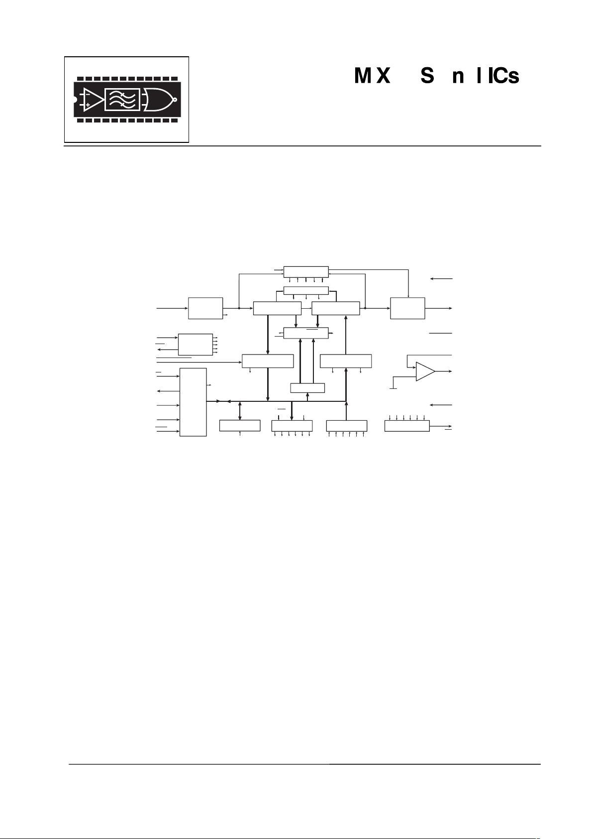
The MX809 is an intelligent, half-duplex 1200-baud MSK Modem, which operates under C-BUS control. This
modem provides software selectable checksum generation and error checking in accordance with MPT1327.
In TX Mode the MX809 will:
1. a) Accept from the host and transmit 8-bit bytes of data as instructed (preamble, sync, address, and data), or
b) Internally calculate and inset a 2 byte checksum based on the preceding 6 bytes f data, or
c) Disable the internal checksum generator and continuously transmit the data supplied.
2. Transmit 1 hang-bit and go to TX idle when all loaded data bytes have been transmitted.
In RX Mode the MX809 will:
1. Detect and carry out bit synchronization within 16 bits.
2. a) Search and detect the user-programmed Sync (or its opposite logic sense) Word and carry out frame
synchronization. Data will then be output in 8-bit bytes via the RX Data Buffer.
b) Use the received checksum to calculate the presence of any errors, setting the Status Register accordingly.
3. Make the incoming data directly available via the RX Data Buffer (RX Freeformat), overriding the synchronization
requirements.
RX input timing is achieved by recovering an RX clock from the incoming data stream. Output tones are
timed to the internally generated TX clock. Filter, register clocks, and transmit MSK tone frequencies are
derived internally from the external Xtal or clock pulse input.
A 4.032MHz Xtal or clock input is required for compliance with the MPT1327 Signaling Specification. Note:
All information contained in this data bulletin is specified using a 4.032MHz Xtal, 1200bps baud rate, with
Mark and Space frequencies of 1200Hz and 1800Hz. The MX809 has a non-committed amplifier on-chip for
general applications in the DBS 800 series.
The MX809 may be used with a 5.0V power supply and is available in the following packages:
24-pin PLCC (MX809LH), and 24-pin CERDIP (MX809J).
Page 2

MSK Modem 2 MX809
1998 MX-COM, Inc. www.mxcom.com Tel: 800 638 5577 336 744 5050 Fax: 336 744 5054 Doc. # 20480036.004
4800 Bethania Station Road, Winston-Salem, NC 27105-1201 USA All trademarks and service marks are held by their respective companies.
Contents
Section Page
1 Block Diagram................................................................................................................3
2 Signal List.......................................................................................................................4
3 External Components....................................................................................................6
4 General Description.......................................................................................................7
5 Controlling Protocol......................................................................................................7
5.1 Address/Commands............................................................................................................ 7
5.2 Address Select .................................................................................................................... 8
5.3 Write to Control Register ..................................................................................................... 9
5.4 RX Data buffer -- “Read RX Data Buffer” ............................................................................ 9
5.5 TX Data Buffer -- “Write to TX Data Buffer”....................................................................... 10
5.6 SYNC Program -- “Write to SYNC Program”..................................................................... 10
5.7 Read Status Register ........................................................................................................ 10
5.8 Interrupt Request............................................................................................................... 11
5.9 General Reset ................................................................................................................... 11
6 Application ................................................................................................................... 12
6.1 Checksum Generation and Checking................................................................................ 12
6.1.1 Generation..............................................................................................................................12
6.1.2 Checking.................................................................................................................................12
6.2 Modem Performance......................................................................................................... 12
6.3 Modem Timing Information................................................................................................ 13
6.4 TX Timing .......................................................................................................................... 14
6.4.1 TX More Than One Message, SYNC Before Every Message, TX Checksum Enabled .........14
6.4.2 TX More Than One Message, TX Checksum Not Enabled. ...................................................14
6.4.3 TX One Message, TX Checksum Enabled .............................................................................15
6.4.4 TX One Message, TX Checksum Not Enabled.......................................................................15
6.5 RX Timing.......................................................................................................................... 16
6.5.1 RX
SYNCSYNC
/ Required Before Every Message, Rx Checksum Not Enabled ................. 16
6.5.2 RX Additional Data Follows Initial Address (6 Data & 2 Checksum Bytes) Data, RX checksum
Enabled...................................................................................................................................16
7 Performance Specifications........................................................................................17
7.1 Electrical Specifications..................................................................................................... 17
7.1.1 Absolute Maximum Limits.......................................................................................................17
7.1.2 Operating Limits......................................................................................................................17
7.1.3 Operating Characteristics .......................................................................................................18
7.1.4 Timing.....................................................................................................................................20
7.2 Packages........................................................................................................................... 21
MXCOM, Inc. reserves the right to change specifications at any time without notice.
Page 3

MSK Modem 3 MX809
1998 MX-COM, Inc. www.mxcom.com Tel: 800 638 5577 336 744 5050 Fax: 336 744 5054 Doc. # 20480036.004
4800 Bethania Station Road, Winston-Salem, NC 27105-1201 USA All trademarks and service marks are held by their respective companies.
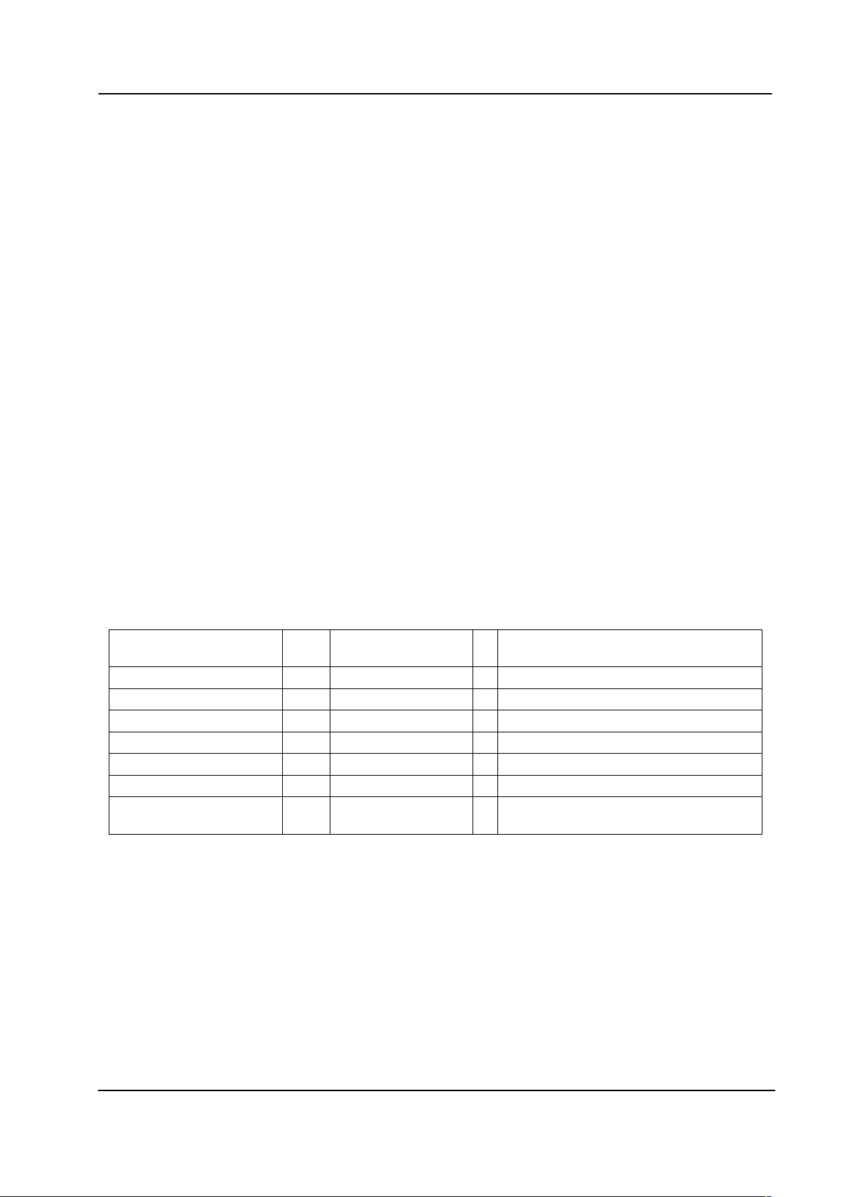
1 Block Diagram
ä
ä
ä
ää
ä
ä
ää
ä
ä
ä
MSK
RECEIVER
CLOCK
GENERA T OR
CHECKSUM
GEN/CHECK
BYTE COUNTER
SYNC/
DETECT
SYNC
DATA REGISTER 1 DATA REGISTER 2
MSK
TRANSMITTER
UNCOMMITTED
AMPLIFIER
INTERRUPT
GENERA T OR
IRQ
AMP OUT
AMP IN
ST ATUS
REGISTER
C-BUS
INTERFACE
AND
CONTROL
LOGIC
RX DATA BUFFER TX DATA BUFFER
8-BIT PARALLEL BUS
TX OUT
V
V
V
V
DD
SS
BIAS
BIAS
RECOVERED
CLOCK
RX IN
XT AL/
CLOCK
XT AL
CS
RX FREEFORMA T
REPLY
DAT A
SERIAL
CLOCK
COMMAND
DAT A
WAKE
CONTROL
REGISTER
ADDRESS
DECODER
ADDRESS
SELECT
SYNC PROGRAM
LOW - HIGH
+
_
INTERRUPT
ENABLE
RX DATA
READY
RX
DETECT
SYNC
RX
DETECT
SYNC
RX SYNC
DETECT
RX SYNC
DETECT
TX DATA
READY
TX IDLE
RECOVERED
CLOCK
Figure 1: Block Diagram
Page 4
MSK Modem 4 MX809
1998 MX-COM, Inc. www.mxcom.com Tel: 800 638 5577 336 744 5050 Fax: 336 744 5054 Doc. # 20480036.004
4800 Bethania Station Road, Winston-Salem, NC 27105-1201 USA All trademarks and service marks are held by their respective companies.
2 Signal List
Pin Signal Description
1
Xtal
This is the output of the on-chip clock oscillator. External components are
required at this output when a Xtal is used. See Figure 2. Inset
2 Xtal/Clock
This is the input to the on-chip clock oscillator inverter. A Xtal or externally
derived clock should be connected here. See Figure 2. Inset
3
IRQ
The output of this pin indicates an interrupt condition to the microcontroller by
going to a logic “0”. This is a “wire-or-able” output that enables the connection of
up to 8 peripherals to 1 interrupt port on the microcontroller. This pin is an opendrain output, and therefore has a low impedance pulldown to logic “0” when active
and a high impedance when inactive. The conditions that cause interrupts are
indicted in the Status Register and are shown in Table 2. The system
IRQ
line
requires a pull-up resistor to V
DD
.
4 N/C
5 N/C
6
Freeformat RX
When this input is logic “0” in the RX Mode, it allows received data to be read
from the RX Data Buffer via the Reply Data line without having to achieve byte
synchronization (SYNC/
SYNC) first. Data will continue to be available after this
input goes to a logic “1” until either a SYNC or
SYNCPrime Bit is set or the
modem is set to TX Mode. When held at a logic “1” the modem operates
normally. This pin has an internal 1M pull-up resistor.
Note
: If this input is held at a logic “0” in the TX Mode, the RX Data Ready bit in
the Status Register may occasionally be set, but not cause an interrupt. If this
input is a logic “0” when going into the RX Mode, and RX Data Ready interrupt
may be generated immediately (in this case the first byte of RX data should be
ignored).
7V
BIAS
The internal circuitry bias line, this is held at VDD/2. This pin must be decoupled
to V
SS
by capacitor C3. See Figure 2.
8 Amp In The inverting input to the on-chip uncommitted amplifier.
9 Amp Out The output of the on-chip uncommitted amplifier.
10 RX In This is the 1200 baud, 1200Hz/1800Hz received MSK signal input. The input
signal to this pin must be AC coupled via capacitor C4. See Figure 2.
11 N/C
12 V
SS
Negative Supply (GND)
13 TX Out This is the 1200 baud, 1200Hz/1800Hz MSK TX output. When not transmitting
data the output impedance of this pin is high. On power-up this output can be any
level. A General Reset command is required to ensure that this output attains
V
BIAS
initially.
14 N/C
15 N/C
16 N/C
17 Reply Data This is the C-BUS serial data output to the microcontroller. The transmission of
Reply Data bytes is synchronized to the Serial Clock under the
CS
input. This 3state output is held high impedance when not sending data to the microcontroller.
See Section 6 and Section 7.1.4.
18 N/C
19
CS
Select Chip . This is the ‘C-BUS’ data loading control function. This input is
provided by the microcontroller. Data transfer sequences are initiated, completed
or aborted by the
CS signal. See Section 6 and Section 7.1.4.
20 Command Data This is the ‘C-BUS’ serial data input from the microcontroller. Data is loaded to
this device in 8-bit bytes, MSB (bit 7) first and LSB (bit 0) last, synchronized to the
Serial Clock. See Section 6 and Section 7.1.4.
Page 5
MSK Modem 5 MX809
1998 MX-COM, Inc. www.mxcom.com Tel: 800 638 5577 336 744 5050 Fax: 336 744 5054 Doc. # 20480036.004
4800 Bethania Station Road, Winston-Salem, NC 27105-1201 USA All trademarks and service marks are held by their respective companies.
Pin Signal Description
21 Serial Clock
This is the ‘C-BUS’ serial Clock input. This clock, produced by the
microcontroller, is used for transfer timing of commands and data to and from the
MSK Modem. See Section 6 and Section 7.1.4.
22 Address Select This pin enables two MX809s to be used on the same C-BUS, providing full-
duplex operation. When at a logic “1” Address/Command bytes (with the
exception of a General Reset) must have bit 3 set to a logic “1” to address this
device. See Table 5 and Table 6.
23
Wake
This input can be used to reactivate the MX809 from Powersave. The device will
be in Powersave when both this pin and bit 2 of the Control Register are set to
logic “1”. Recovery from Powersave is achieved by putting either the
Wake pin or
the Powersave bit in the Control Register to logic “0”. This allows MX809
activation by the microcontroller or an external signal, such as R.S.S.I. or Carrier
Detect. See Table 3.
24 V
DD
Positive supply. A single +5.0V power supply is required. Levels and voltages
within the MSK Modem are dependent upon this supply.
Table 1: Signal List
TX Idle RX Data Ready TX Data Ready
RX SYNC Detect RX Sync Detect
Interrupt outputs can be disabled by bit 3 of the Control Register
Table 2:
IRQ
Conditions
Powersave (CR bit 2)
Wake
MX809 Condition
1
0
1
0
1
1
0
0
Powersave
Enabled
Enabled
Enabled
Table 3:
Wake
and Powersave Conditions
Page 6
MSK Modem 6 MX809
1998 MX-COM, Inc. www.mxcom.com Tel: 800 638 5577 336 744 5050 Fax: 336 744 5054 Doc. # 20480036.004
4800 Bethania Station Road, Winston-Salem, NC 27105-1201 USA All trademarks and service marks are held by their respective companies.
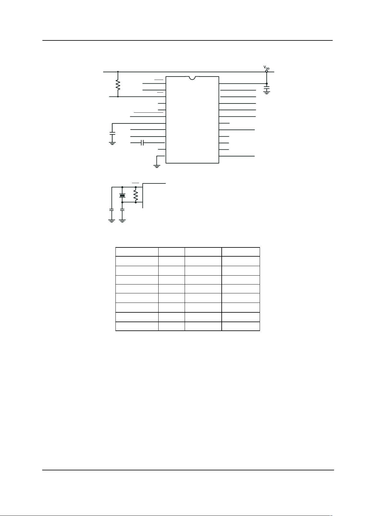
3 External Components
➤
➤
➤
➤
➤
➤
➤
➤
➤
➤
➤
➤
➤
➤
➤
➤
R2
SEE INSET
XTAL
XTAL/CLOCK
IRQ
RX FREEFORMAT
V
BIAS
AMP IN
AMP OUT
C3
1
2
3
4
5
6
7
8
9
10
11
12
13
14
15
16
17
18
19
20
21
22
23
24
MX809J
RX IN
C4
V
SS
V
DD
WAKE
ADDRESS SELECT
SERIAL CLOCK
COMMAND DA TA
CS
REPLY DATA
TX OUT
C5
INSET
XTAL
C2 C1
X1 R1
1
2
XTAL/CLOCK
MX809J
Figure 2: Recommended External Components
Component Notes Value Tolerance
R1
1.0M
±10%
R2
22.0K
±10%
C1 1 33pF ±20%
C2 1 33pF ±20%
C3
1.0F
±20%
C4
0.1F
±20%
C5
1.0F
±20%
X1 1 4.032MHz
Table 4: Recommended External Components
Recommended External Component Notes:
1. Xtal circuit capacitors C1 (CD) and C2 (CG) shown in Inset 2 are recommended in accordance with MXCOM’s Crystal Oscillator Application Note.
Page 7
MSK Modem 7 MX809
1998 MX-COM, Inc. www.mxcom.com Tel: 800 638 5577 336 744 5050 Fax: 336 744 5054 Doc. # 20480036.004
4800 Bethania Station Road, Winston-Salem, NC 27105-1201 USA All trademarks and service marks are held by their respective companies.
4 General Description
The MX809 is an intelligent, half-duplex 1200-baud MSK Modem, which operates under C-BUS control. This
modem provides software selectable checksum generation and error checking in accordance with MPT1327.
In TX Mode the MX809 will:
1. a) Accept from the host and transmit 8-bit bytes of data as instructed (preamble, sync, address, and data), or
b) Internally calculate and inset a 2 byte checksum based on the preceding 6 bytes of data, or
c) Disable the internal checksum generator and continuously transmit the data supplied.
2. Transmit 1 hang-bit and go to TX idle when all loaded data bytes have been transmitted.
In RX Mode the MX809 will:
1. Detect and carry out bit synchronization within 16 bits.
2. a) Search and detect the user-programmed Sync (or its opposite logic sense) Word and carry out frame
synchronization. Data will then be output in 8-bit bytes via the RX Data Buffer.
b) Use the received checksum to calculate the presence of any errors, setting the Status Register accordingly.
3. Make the incoming data directly available via the RX Data Buffer (RX Freeformat), overriding the synchronization
requirements.
RX input timing is achieved by recovering an RX clock from the incoming data stream. Output tones are
timed to the internally generated TX clock. Filter, register clocks, and transmit MSK tone frequencies are
derived internally from the external Xtal or clock pulse input.
A 4.032MHz Xtal or clock input is required for compliance with the MPT1327 Signaling Specification. Note:
All information contained in this data bulletin is specified using a 4.032MHz Xtal, 1200bps baud rate, with
Mark and Space frequencies of 1200Hz and 1800Hz. The MX809 has a non-committed amplifier on-chip for
general applications in the DBS 800 series.
5 Controlling Protocol
Control of the functions within the MX809 MSK Modem is by a group of Address/Commands and appended
data instructions from the system microcontroller. Two separate MSK Modems can be addressed. The use
of these A/Cs is detailed in the following paragraphs and tables.
Command Assignment Address/Command
Binary
Command Data
HEX
MSB LSB
General Reset 01 00000001 Control Register bits set to logic “0”
Write to Control Register 40 01000000 + 1 byte instruction to Control Register
Read Status Register 41 01000001 + 1 byte reply from Status Register
Read RX Data Buffer 42 01000010 + 1 byte of data from RX Data Buffer
Write to TX Data Buffer 43 01000011 + 1 byte of data to TX Data Buffer
Write to SYNC Program 44 01000100 + 2 bytes of SYNC Word to SYNC
Program. Register
Table 5: Modem No. 1 C-BUS Address/Commands – (Address Select input at a logic “0”)
5.1 Address/Commands
Instructions and data transactions to and from the MX809 consist of an Address/Command (A/C) byte
followed by either further instructions or data, or a Status or RX Data Reply.
Control and configuration is by writing instructions from the microcontroller to the Control Register [40
H
(48H)].
Reporting of the MX809 configuration is by reading the Status Register [41
H
(49H)]. Instructions and data are
transferred via C-BUS in accordance with the timing information given in Figure 11.
Data to be transmitted as MSK is sent to the TX Data Buffer via the Command Data line. Received data is
read from the RX Data buffer via the Reply Data line.
Instructions and data transactions to and from this device are preceded by the relevant A/C.
Page 8

MSK Modem 8 MX809
1998 MX-COM, Inc. www.mxcom.com Tel: 800 638 5577 336 744 5050 Fax: 336 744 5054 Doc. # 20480036.004
4800 Bethania Station Road, Winston-Salem, NC 27105-1201 USA All trademarks and service marks are held by their respective companies.
C-BUS allocations for the MX809 are shown in Table 5 and Table 6.
Command Assignment Address/Command
Binary
Command Data
HEX
MSB LSB
General Reset 01 00000001 Control Register bits set to logic “0”
Write to Control Register 48 01001000 + 1 byte instruction to Control Register
Read Status Register 49 01001001 + 1 byte reply from Status Register
Read RX Data Buffer 4A 01001010 + 1 byte of data from RX Data Buffer
Write to TX Data Buffer 4B 01001011 + 1 byte of data to TX Data Buffer
Write to SYNC Program 4C 01001100 + 2 bytes of SYNC Word to SYNC
Program Register
Table 6: Modem No. 2 C-BUS Address/Commands – (Address Select input at a logic “1”)
5.2 Address Select
This input allows 2 MSK Modems on the same BUS, using the correct addressing.
When operating in a system using 2 MSK Modems, one MSK Modem is designated No. 1 and requires its
Address Select input to be held at a logic “0”. The second Modem (No. 2) requires its Address select input to
be held at logic “1”.
All C-BUS transactions with Modem 1 will use Address/Command allocations 40
H
to 44H (Table 5) and
transactions with Modem 2 will use 48
H
to 4CH (Table 6).
For explanation purposes, further descriptions of MX809 MSK Modem internal register functions will deal
primarily with MSK Modem No. 1 (Address Select at logic “0”).
Page 9

MSK Modem 9 MX809
1998 MX-COM, Inc. www.mxcom.com Tel: 800 638 5577 336 744 5050 Fax: 336 744 5054 Doc. # 20480036.004
4800 Bethania Station Road, Winston-Salem, NC 27105-1201 USA All trademarks and service marks are held by their respective companies.
5.3 Write to Control Register
This “Write Only” register directs the Modem’s operation.
SYNC:
When set, this bit enables
SYNCWord detection. It is cleared on a successful SYNC Word
detection.
SYNC Prime:
When set, this bit enables SYNC Word detection. It is cleared on a successful SYNC Word
detection.
Interrupt Enable:
When set, this bit allows interrupts to be output by the MX809 on the
IRQ line.
Powersave:
Used in conjunction with the
Wake input (see Section 2) to control the Powersave state of the
MX809.
Checksum Enable:
When set:
In TX
: A 2-byte checksum is generated and transmitted after every 6 bytes transmitted.
In RX
: After every 8 received bytes (6 information + 2 checksum) the checksum word is checked. If
the checksum is correct, the RX Checksum True bit in the Status Register is set to a logic “1”. When
this bit is a logic “0” no checksum are generated or checked.
Note:
Checksum operation is inhibited during the
SYNC/SYNC search period.
Setting Control bits
MSB
Transmitter first
Bit 7
Not Used
Set to “0”
6
Not Used
Set to “0”
5
SYNC
Prime
0
1 Primed
4 SYNC Prime
0
1 Primed
3 Interrupt Enable
0
1
Disable
Enable
2 Powersave
0
1
Normal Operation
Powersave
1 Checksum Enable
0
1
Disable
Enable
0 RX/TX Mode
0
1
RX
TX
Table 7: Control Register
5.4 RX Data buffer -- “Read RX Data Buffer”
This “Read Only” register contains the last byte of data received from the Data Register. Data is received Bit
7 (MSB) first.
MSB LSB
7 654321 0
RX Data Buffer
Page 10

MSK Modem 10 MX809
1998 MX-COM, Inc. www.mxcom.com Tel: 800 638 5577 336 744 5050 Fax: 336 744 5054 Doc. # 20480036.004
4800 Bethania Station Road, Winston-Salem, NC 27105-1201 USA All trademarks and service marks are held by their respective companies.
5.5 TX Data Buffer -- “Write to TX Data Buffer”
This “Write Only” register contains the next byte of data to be transmitted. Bit 7 (MSB) is transmitted first.
MSB LSB
7 654321 0
TX Data Buffer
5.6 SYNC Program -- “Write to SYNC Program”
This “Write Only” register is loaded with the required SYNC word. This word (or its opposite logic sense,
SYNC
) is compared with the received synchronization word. If the required SYNC Word is less that 16bits,
the remaining bits must be programmed as preamble (10101010…etc). Bit 15 (MSB) is loaded first.
MSB
Byte 1 Byte 2
LSB
15 14 13 12 11 10 9 8 7 6 5 4 3 2 1 0
SYNC High SYNC Low
5.7 Read Status Register
This “Read Only” register indicated the source of MX809 interrupts (
sIRQ
).
RX
SYNC Detect:
This is set and an Interrupt is generated when the correct
SYNCWord is detected (if
SYNC
Prime is set).
It is cleared by (1) reading the Status Register, and (2) setting
TX/RX to logic “1”.
RX SYNC Detect:
This is set and an Interrupt is generated when the correct SYNC Word is detected (if
SYNC Prime is set).
It is cleared by (1) reading the Status Register, and (2) setting
TX/RX to logic “1”.
TX Idle:
This is set and an Interrupt is generated when all loaded TX data and 1 “hang-bit” have been
transmitted.
It is cleared by (1) writing to the TX Data Buffer, and (2) setting
TX/RX to logic “0”.
TX Data Ready:
This is set and an Interrupt generated indicating that a byte of data should be written to the
TX Data Buffer.
It is cleared by (1) reading the Status Register and writing a byte of data to the TX Data Buffer, and (2) setting
TX/RX to logic “0”.
RX Data Ready:
When this is set and an Interrupt generated, it indicates that the RX Data Buffer is full, and
that a byte of data is to be read from the RX Data buffer. This must be read within 8 bit periods.
It is cleared by (1) reading the Status Register and the RX Data buffer, and (2) setting the
TX/RX to logic “1”/
RX Checksum True:
This is set and an Interrupt is generated by a successful comparison of the received
and self-generated checksums.
It is cleared by (1) reading the Status Register and the RX Data Buffer, and (2)
TX/RX being taken to logic
“1”
Page 11

MSK Modem 11 MX809
1998 MX-COM, Inc. www.mxcom.com Tel: 800 638 5577 336 744 5050 Fax: 336 744 5054 Doc. # 20480036.004
4800 Bethania Station Road, Winston-Salem, NC 27105-1201 USA All trademarks and service marks are held by their respective companies.
Reading Status Bits
MSB Received First
Bit 7 Undefined
0
1
“0” or
“1”
6 Undefined
0
1
“0” or
“1”
5
RX
SYNC Detect
0
1
SYNC
4 RX SYNC Detect
0
1SYNC
3 TX Idle
0
1Idle
2 TX Data Ready
0
1 TX Date Ready
1 RX Checksum True
0
1True
0 RX Data Ready
0
1 RX Data Ready
Table 8: Status Register
5.8 Interrupt Request
The conditions that cause interrupts to be output (if enabled by the Control Register) from the MX809 are:
TX Idle
TX Data Ready
RX
SYNCDetect
RX Data Ready
RX SYNC Detect
The Status Register should be read to find the cause of the interrupt. Interrupts are cleared by (1) reading the
Status Register, or (2) changing the state of the
TX/RX
bit.
5.9 General Reset
Upon power-up, the bits in the MX809 Mode register and buffer will be random (either “0” or “1”). The
General Reset command (01
H
) will “reset” all microcircuits in the C-BUS and had the following effect on the
MX809.
All bits in the Control Register will be set to logic “0”. The Tx Out output will be set to V
BIAS
.
Note
: The Status register, RX Data Buffer, TX Data Buffer, and SYNC Program register are not affected by
the General Reset Command.
Page 12

MSK Modem 12 MX809
1998 MX-COM, Inc. www.mxcom.com Tel: 800 638 5577 336 744 5050 Fax: 336 744 5054 Doc. # 20480036.004
4800 Bethania Station Road, Winston-Salem, NC 27105-1201 USA All trademarks and service marks are held by their respective companies.
6 Application
6.1 Checksum Generation and Checking
6.1.1 Generation
The checksum generator takes the 48 bits from the 6 bytes loaded into the TX Data Buffer and divides them
into modulo-2 by the generating polynomial:
x
15
+ x14 + x13 + x11 + x4 + x2 + x
1
It then takes the 15-bit remainder from the polynomial divider, inverts the last bit and appends an EVEN parity
bit generated from the initial 48 bits and the 15 bit remainder (with the last bit inverted). This 16 bit word is
used as the “Checksum”.
6.1.2 Checking
The checksum checker does two things:
1. It takes the first 63 bits of a received message, inverts bit 63, and divides them modulo-2 by the
generating polynomial:
x
15
+ x14 + x13 + x11 + x4 + x2 + x
1
2. The 15 bits remaining in the polynomial divider are checked to make sure that they are all zero.
3. It generates an even parity bit from the first 63 bits of a received message and compares this bit with the
received parity (bit 64).
If the 15 bits in the polynomial divider are all zero and the two parity bits are equal, then the RX
Checksum True (Status Register bit 1) is set.
6.2 Modem Performance
Figure 3: Bit Error Rate vs. Signal-to-Noise Ratio
Page 13

MSK Modem 13 MX809
1998 MX-COM, Inc. www.mxcom.com Tel: 800 638 5577 336 744 5050 Fax: 336 744 5054 Doc. # 20480036.004
4800 Bethania Station Road, Winston-Salem, NC 27105-1201 USA All trademarks and service marks are held by their respective companies.
6.3 Modem Timing Information
Figure 4: Modem Timing
Notes:
1. The SYNC and
SYNCdetector searches the incoming bit stream starting at the end of the byte in which
SYNC/SYNC
Prime was set.
2. After detection of a
SYNC/SYNC word, the SYNC/SYNC Prime bits automatically go low (control bits 5
and 6: detector off.
3. The checksum checker is inhibited during the time
SYNC/SYNC search is operating.
4. The Status Register will indicate whether SYNC or
SYNC
was detected here.
5. Any number of preamble bits can occur here.
6. Any number of bits can occur here.
7.
Freeformat RX set high.
Page 14

MSK Modem 14 MX809
1998 MX-COM, Inc. www.mxcom.com Tel: 800 638 5577 336 744 5050 Fax: 336 744 5054 Doc. # 20480036.004
4800 Bethania Station Road, Winston-Salem, NC 27105-1201 USA All trademarks and service marks are held by their respective companies.
6.4 TX Timing
A – Address bytes
C – Checksum bytes
D – Data bytes
H – Hang bit
P – Preamble bytes
- Don’t care state
TX only – In TX, Preamble, and SYNC are
loaded as data from the microcontroller.
6.4.1 TX More Than One Message, SYNC Before Every Message, TX Checksum Enabled
NOTE 6
RX/TX
TX OUTPUT
IRQ
READ ST ATUS
REGISTER
TX DAT A READY
WRITE TO
TX DAT A BUFFER
CHECKSUM
ON/OFF
P1 P2 P
P1 P2 P
S1 S2 A1 A2 A3 A4 A5 A6
C1 C2 S1 S2 D1 D2 D3 D4 D5 D6
S1 S2 A1 A2 A3 A4 A5 A6 S2
S1
D1 D2 D3 D4 D5 D6
Figure 5: TX More Than One Message, SYNC Before Every Message, TX Checksum Enabled
Notes:
1. Preamble and SYNC bytes are loaded as data from the microcontroller.
2. The TX output will be held at bias level when no data is being transmitted.
3. TX byte synchronization is established by loading of the first preamble byte from the microcontroller.
4. Checksum must be turned off during preamble and SYNC words.
5. When
TX/RX is low, TX output is at bias.
6. Any number of preamble bytes can occur here.
6.4.2 TX More Than One Message, TX Checksum Not Enabled.
NOTE 2 NOTE 3 NOTE 3
RX/TX
TX OUTPUT
IRQ
READ STATUS
REGISTER
TX DATA READY
WRITE TO
TX DAT A BUFFER
CHECKSUM
ON/OFF
P1 P2 P
P1 P2 P
S1 S2 A1 A2 A3 A4 A S1 S2 D1 D2 D3 D4 D S1 S2 D1
S1 S2 A1 A2 A3 A4 A S1 S2 D1 D2 D3 D S1 S2 D1 D2
D4
Figure 6: TX More Than One Message, TX Checksum Not Enabled.
Notes:
1. Preamble, SYNC words and checksums are supplied by the microcontroller in this format as data bytes.
2. Any number of preamble bytes can occur here.
3. Any number of address/data bytes can occur here.
Page 15

MSK Modem 15 MX809
1998 MX-COM, Inc. www.mxcom.com Tel: 800 638 5577 336 744 5050 Fax: 336 744 5054 Doc. # 20480036.004
4800 Bethania Station Road, Winston-Salem, NC 27105-1201 USA All trademarks and service marks are held by their respective companies.
6.4.3 TX One Message, TX Checksum Enabled
NOTE 2
RX/TX
TX OUTPUT
IRQ
READ STATUS
REGISTER
TX DATA READY
WRITE TO
TX DATA BUFFER
CHECKSUM
ON/OFF
TX IDLE
P1
P1
S1
S1
P2 P
S2
A1 A2 A3 A4 A5 A6
C1 C2
H
PP2
A6A5A4A3A2A1
S2
Figure 7: TX One Message, TX Checksum Enabled
Notes:
1. H is the “Hangover bit” (Logic1) appended to the transmitted message before transmission is terminated.
2. Any number of preamble bytes can occur here.
3. Transmission terminates after C1, C2, and H. Termination occurs when no further data bytes are written
to the TX Data Buffer.
6.4.4 TX One Message, TX Checksum Not Enabled.
NOTE 2
RX/TX
TX OUTPUT
IRQ
READ STATUS
REGISTER
TX DA TA READ Y
WRITE TO
TX DA TA BUFFER
CHECKSUM
ON/OFF
TX IDLE
P1
P1
S1
S1
NOTE 3
A
PP2
HAA5A4A3A2A1
S2
A5A4A3A2
S2
A1
PP2
Figure 8: TX One Message, TX Checksum Not Enabled
Notes:
1. H is the “Hangover bit” (Logic1) appended to the transmitted message before transmission is terminated.
2. Any number of preamble bytes can occur here.
3. Any number of address/data bytes can occur here.
4. Transmission terminates when no further data bytes are loaded into the TX Data Buffer.
Page 16

MSK Modem 16 MX809
1998 MX-COM, Inc. www.mxcom.com Tel: 800 638 5577 336 744 5050 Fax: 336 744 5054 Doc. # 20480036.004
4800 Bethania Station Road, Winston-Salem, NC 27105-1201 USA All trademarks and service marks are held by their respective companies.
6.5 RX Timing
A – Address bytes
C – Checksum bytes
D – Data bytes
H – Hang bit
P – Preamble bytes
- Don’t care state
TX only – In TX, Preamble, and SYNC are
loaded as data from the microcontroller.
6.5.1 RX
SYNCSYNC
/
Required Before Every Message, Rx Checksum Not Enabled
NOTE 1 NOTE 2 NOTE 3
P1 P2 P
A1 A2 A3
A1 A2 A3 A
A1 A2 A3 A
SYNCSYNC
RX/TX
RX INPUT
IRQ
READ STATUS REGISTER
SYNC DETECT
(OR DETECT)SYNC
RX DA TA READY
READ RX DA TA BUFFER
SYNC/ PRIMESYNC
CHECKSUM ON/OFF
Figure 9: RX
SYNCSYNC
/
Required Before Every Message, RX Checksum not Enabled
Notes:
1. Any number of preamble bits can occur here.
2. Any number of address/data bytes can occur here.
3. Any number of bits can occur here
4.
FreeformatRX
set high.
6.5.2 RX Additional Data Follows Initial Address (6 Data & 2 Checksum Bytes) Data, RX checksum
Enabled
NOTE 1
SYNC
RX/TX
RX INPUT
IRQ
READ STATUS
REGISTER
RX DATA READY
SYNC DETECT
(OR
DETECT)
SYNC
READ RX
DA TA BUFFER
RX CHECKSUM
TRUE
SYNC/
PRIME
SYNC
CHECKSUM
ON/OFF
P1 P2 P
A1 A2 A3 A4 A5 A6 C1 C2 D1 D2 D3 D4 D5 D6 C1 C2 D1
Figure 10: RX Additional Data Follows Initial Address (6 Data & 2 Checksum Bytes) Data , RX
Checksum Enabled
Notes:
1. Any number of preamble bits can occur here.
2.
FreeformatRX
set high.
Page 17

MSK Modem 17 MX809
1998 MX-COM, Inc. www.mxcom.com Tel: 800 638 5577 336 744 5050 Fax: 336 744 5054 Doc. # 20480036.004
4800 Bethania Station Road, Winston-Salem, NC 27105-1201 USA All trademarks and service marks are held by their respective companies.
7 Performance Specifications
7.1 Electrical Specifications
7.1.1 Absolute Maximum Limits
Exceeding these maximum ratings can result in damage to the device.
General Notes Min. Typ. Max. Units
Supply (VDD-VSS) -0.3 7.0 V
Voltage on any pin to V
SS
-0.3 VDD + 0.3 V
Current
V
DD
-30 30 mA
V
SS
-30 30 mA
Any other pin -20 20 mA
J / LH Packages
Total allowable Power dissipation
at T
AMB
= 25C
800 mW
Derating above 25C
10
mW/C above 25C
Operating Temperature -40 85
C
Storage Temperature -55 125
C
Table 9: Absolute Maximum Ratings
7.1.2 Operating Limits
Correct Operation of the device outside these limits is not implied.
Notes Min. Typ. Max. Units
Supply (VDD-VSS) 4.5 5.0 5.5 V
Operating Temperature -40 85
C
Xtal Frequency 4.032 MHz
Table 10: Operating Limits
Page 18

MSK Modem 18 MX809
1998 MX-COM, Inc. www.mxcom.com Tel: 800 638 5577 336 744 5050 Fax: 336 744 5054 Doc. # 20480036.004
4800 Bethania Station Road, Winston-Salem, NC 27105-1201 USA All trademarks and service marks are held by their respective companies.
7.1.3 Operating Characteristics
For the following conditions unless otherwise specified.
V
DD
= 5.0V @ T
AMB
= 25C
Xtal/Clock Frequency = 4.032MHz, Audio Level 0dB ref. = 308mV
RMS
@ 1kHz
Bit Rate = 1200bps
Notes Min. Typ. Max. Units
Static Values
Supply Current
Enabled 5.0 mA
Powersave 2.0 mA
Dynamic Values
Digital Interface
Input Logic “1” 1 3.5 V
Input Logic “0” 1 1.5 V
Output Logic “1” (IOH = -120A)
2 4.6 V
Output Logic “0” (IOH = 360A)
2, 3 0.4 V
Digital Input Current
VIN = Logic “1” or “0” 1 1.0
A
Digital Input Capacitance 1 7.5 pF
Tri-State “OFF” Leakage Current 8 -4.0 4.0
A
Analog Impedance
Input Impedance 100
k
Output Impedance
Transmitting Data 6.0 10.0
k
Not Transmitting Data 1.0
k
On-Chip Xtal Oscillator
R
IN
10.0
M
R
OUT
5.0
k
Gain 15.0 dB
Frequency 4 4.032 MHz
Receiver
Signal Input Levels 5 -9.0 -2.0 10.5 dB
Bit Error Rate
At 12dB SNR 7.0 10
-4
At 20dB SNR 1.0 10
-8
Synchronization at 12dB SNR 6
Probability of Bit 8 being correct 99.0 %
Probability of Bit 16 being correct 99.5 %
Page 19

MSK Modem 19 MX809
1998 MX-COM, Inc. www.mxcom.com Tel: 800 638 5577 336 744 5050 Fax: 336 744 5054 Doc. # 20480036.004
4800 Bethania Station Road, Winston-Salem, NC 27105-1201 USA All trademarks and service marks are held by their respective companies.
Notes Min. Typ. Max. Units
Transmitter
Output Level 0 dB
Output Level Variation -1.0 1.0 dB
Output Distortion 3.0 5.0 %
Third Harmonic Distortion 2.0 3.0 %
Logic “1” Frequency 7 1200 Hz
Logic “0” Frequency 7 1800 Hz
Isochronous Distortion
1200Hz – 1800Hz 25.0 40.0
s
1800Hz – 1200Hz 20.0 40.0
s
Uncommitted Amplifier
Bandwidth 200 kHz
Gain 50.0 dB
Input Impedance 1.0
Output Impedance 10.0
k
Table 11: Operating Characteristics
Operating Characteristics Notes:
1. Device control pins: Serial Clock, Command Data,
Wake , and CS.
2. Reply Data output.
3.
IRQ output
4. For baud rate specified (1200 baud)
5. Signal-to-Noise Ratio = 50dB
6. The response time is measured using 10101010…101 signal input pattern at 230mV
RMS
(-2.5dB) with
noise.
7. Dependant upon Xtal tolerance.
8.
IRQ
and Reply Data outputs for V
SS
< V
OUT
< VDD.
Page 20

MSK Modem 20 MX809
1998 MX-COM, Inc. www.mxcom.com Tel: 800 638 5577 336 744 5050 Fax: 336 744 5054 Doc. # 20480036.004
4800 Bethania Station Road, Winston-Salem, NC 27105-1201 USA All trademarks and service marks are held by their respective companies.
7.1.4 Timing
C-BUS Timing Min. Typ. Max. Units
t
CSE
Chip Select Low to First Serial Clock Rising Edge 2.0
s
t
CHS
Last Serial Clock Rising Edge to Chip Select High 4.0
s
t
HIZ
Chip Select High to Reply Data High -Z 2.0
t
CSOFF
Chip Select High time between transactions 2.0
s
t
NXT
Inter-Byte Time 4.0
s
t
CK
Serial Clock Period 2.0
s
Table 12: Timing Information
Notes:
1. Depending on the command, 1 or 2 bytes of Command Data is transmitted to the peripheral MSB (bit 7)
first, LSB (bit 0) last. Reply Data is read from the peripheral MXB (bit 7) first, LSB (bit 0) last.
2. Data is clocked into and out of the peripheral on the rising Serial Clock edge.
3. Loaded commands are acted upon at the end of each command.
4. To allow for differing microcontroller serial interface formats, C-BUS compatible ICs are able to work with
either polarity Serial Clock pulses.
CHIP SELECT
SERIAL CLOCK
COMMAND DAT A
REPLY DATA
ADDRESS/COMMAND
BYTE
FIRST DATA BYTE LAST DATA BYTE
FIRST REPLY DAT A BYTE LAST REPLY DAT A BYTE
Logic level is not important
MSB LSB
76543210
MSB LSB
76543210
MSB LSB
76543210
76543210
76543210
MSB LSB MSB LSB
t
t
t
CSOFF
t
CSH
HIZ
t
NXT
t
NXT
CK
t
CSE
ä
ä
Figure 11: C-BUS Timing Information
Page 21

MSK Modem 21 MX809
1998 MX-COM, Inc. www.mxcom.com Tel: 800 638 5577 336 744 5050 Fax: 336 744 5054 Doc. # 20480036.004
4800 Bethania Station Road, Winston-Salem, NC 27105-1201 USA All trademarks and service marks are held by their respective companies.
7.2 Packages
NOTE: All dimensions in inches (mm.)
Angles are in degrees
PackageTolerances
A
B
C
E
E1
H
TYP. MAX.MIN.DIM.
J
J1
P
Y
T
K
L
0.220 (5.59)
0.555 (14.04)
0.670 (17.02)
7°
0.160 (4.05)
1.270 (32.26)
0.151 (3.84)
0.100 (2.54)
0.121 (3.07)
0.600 (15.24)
0.590 (14.99) 0.625 (15.88)
0.015 (0.38) 0.045 (1.14)
0.008 (0.20) 0.015 (0.38)
0.015 (0.38) 0.023 (0.58)
0.040 (1.02) 0.065 (1.65)
0.066 (1.67) 0.074 (1.88)
1.200 (30.48)
0.500 (12.70)
H
K
L
J1
J1
J
J
P
P
C
C
B
B
A
A
PIN1
PIN1
T
T
E
E
E1
E1
Y
Figure 12: 24-pin CERDIP Mechanical Outline:
Order as part no. MX809J
PackageTolerances
NOTE: All dimensions in inches (mm.)
Angles are in degrees
A
B
C
D
E
H
P
F
G
TYP. MAX.MIN.DIM.
K
J
W
T
Y
0.435 (11.05)
0.435 (11.05)
0.051 (1.30)
0.009 (0.22)
6°
30°
0.409 (10.40)
0.409 (10.40)
0.146 (3.70)
0.417 (10.60)
0.417 (10.60)
0.049 (1.24)
0.006 (0.152)
0.250 (6.35)
0.250 (6.35)
0.023 (0.58)
0.047 (1.19)
0.022 (0.55)0.018 (0.45)
0.380 (9.61)
0.380 (9.61)
0.128 (3.25)
0.048 (1.22)
45°
F
G
P
A
D
B
E
PIN 1
W
C
J
K
Y
W
H
T
Figure 13: 24-pin PLCC Mechanical Outline:
Order as part no. MX809LH
 Loading...