

Page 1
DATA BULLETIN
MX806A
Audio Processor
1998 MX-COM, Inc. www.mxcom.com Tel: 800 638 5577 336 744 5050 Fax: 336 744 5054 Doc. # 20480064.006
4800 Bethania Station Road, Winston-Salem, NC 27105-1201 USA All trademarks and service marks are held by their respective companies.
Features
Half-Duplex Audio Processor
Dynamic Control of Signal Levels
Performs Signal Conditioning and
Filtering requirements for both
Transmit and Receive
Three separate signal sections:
Input process
Main Process
Mixing and Output Drives
Low Power Operation
Member of DBS800 Family (C-BUS
Compatible)
C-BUS INTERFA CE
MIC. AMP
VOGAD AMP
HIGHPASS
FILTER
GAIN
SET
PRE-EMPHASIS
LIMITING
FILTERING
GAIN SETTING
MODULATION
MIXER AMP
VOGAD
SENSE
VOGAD
SENSE
OR
MAIN PROCESS
CLOCK
GENERAT OR
BUFFER
ATTENUAT OR
ATTENUAT OR
ATTENUAT OR
INPUT
PROCESS
DE-EMPHASIS
FILTER
OUTPUT DRIVES
#
#
#
#
#
## #
#
#
#
#
LOUDSPEAKER
AUDIO
MODULATION 2
OUT
MODULATION 1
OUT
TRANSMITTER
MODULATION
DRIVES
MOD
OUT
MOD
IN
MAIN
PROCESS
OUT
PRIMARY
AND
SECONDARY
AUDIO
INPUTS
Voice
Sub-Audio
Tone
MSK,etc.
COMMAND
DATA
SERIAL
CLOCK
CHIP
SELECT
VOGAD SENSE
CALIBRATION INPUT
TX
MIC IN
RX
AUDIO IN
XTAL/CLOCK
XTAL
TO EXTERNAL
AUDIO PROCESSES
EXTERNAL AUDIO
PROCESS IN
POWER
SUPPL Y
The MX806A LMR audio processor is intended too primarily to operate as the “Audio Terminal” or radio
systems using the DBS800 Digitally Integrated Baseband Subsystem.
The MX806A half-duplex device has signal paths and level setting elements that are configured and adjusted
by digital information sent from the radio microcontroller using C-BUS protocol. (C-BUS is the serial interface
for all DBS 800 ICs.)
The Signal Path is divided into three sections: Input Process, Main process, and Mixing and Output Drives.
If selected, signal level stability and output accuracy of the MX806A is maintained by a voltage-controlled gain
system using selectable signal-level detectors. Signal levels can be dynamically controlled to provide
“dynamic compensation” for factors such as temperature drift, VCO non-linearity, etc.
The MX806A audio stages can be completely disabled – or the whole IC can be placed into powersave mode,
leaving only clock and C-BUS circuitry active.
The MX806A may be used with a 5.0V power supply and is available in the following packages:
24-pin SOIC (MX806ADW), 24-pin PLCC (MX806ALH), and 24-pin PDIP (MX806AP).
Page 2

Audio Processor 2 MX806A
1998 MX-COM, Inc. www.mxcom.com Tel: 800 638 5577 336 744 5050 Fax: 336 744 5054 Doc. # 20480064.006
4800 Bethania Station Road, Winston-Salem, NC 27105-1201 USA All trademarks and service marks are held by their respective companies.
Contents
Section Page
1 Block Diagram................................................................................................................3
2 Signal List.......................................................................................................................4
3 External Components....................................................................................................6
4 General Description.......................................................................................................7
4.1 Signal Path .......................................................................................................................... 7
4.2 VOGAD................................................................................................................................ 7
4.2.1 VOGAD Components Calculations – Figure 2 and Figure 5.....................................................8
4.3 Calibration Methods............................................................................................................. 8
4.3.1 TX Calibration: From Mic. In to Modulator Drives Out.............................................................8
4.3.2 RX Calibration: From RX Audio In to Audio Out......................................................................8
5 Controlling Protocol....................................................................................................10
5.1.1 Control Command – (Preceded by A/C 10H)..........................................................................11
5.1.2 Mode Command – (Preceded by A/C 11H)............................................................................12
5.1.3 Modulator Levels – (Preceded by A/C 12H) ........................................................................... 13
5.1.4 Volume Set – (Preceded by A/C 13H)....................................................................................15
6 Application Notes ........................................................................................................16
7 Performance Specifications........................................................................................17
7.1 Electrical Specifications..................................................................................................... 17
7.1.1 Absolute Maximum Limits.......................................................................................................17
7.1.2 Operating Limits......................................................................................................................17
7.1.3 Operating Characteristics .......................................................................................................18
7.1.4 Timing..................................................................................................................................... 21
7.2 Packages........................................................................................................................... 22
MXCOM, Inc. reserves the right to change specifications at any time without notice.
Page 3
Audio Processor 3 MX806A
1998 MX-COM, Inc. www.mxcom.com Tel: 800 638 5577 336 744 5050 Fax: 336 744 5054 Doc. # 20480064.006
4800 Bethania Station Road, Winston-Salem, NC 27105-1201 USA All trademarks and service marks are held by their respective companies.
1 Block Diagram
C-BUS INTERFACE
MIC. AMP
VOGAD AMP
HIGHPASS
FILTER
GAIN
SET
PRE-EMPHASIS
LIMITING
FILTERING
GAIN SETTING
MODULATION
MIXER AMP
VOGAD
SENSE
VOGAD
SENSE
OR
MAIN PROCESS
CLOCK
GENERATOR
BUFFER
ATTENUATOR
ATTENUATOR
ATTENUATOR
INPUT
PROCESS
DE-EMPHASIS
FILTER
OUTPUT DRIVES
#
#
#
#
#
## #
#
#
#
#
LOUDSPEAKER
AUDIO
MODULATION 2
OUT
MODULATION 1
OUT
TRANSMITTER
MODULATION
DRIVES
MOD
OUT
MOD
IN
MAIN
PROCESS
OUT
PRIMARY
AND
SECONDARY
AUDIO
INPUTS
Voice
Sub-Audio
Tone
MSK,etc.
COMMAND
DATA
SERIAL
CLOCK
CHIP
SELECT
VOGAD SENSE
CALIBRATION INPUT
TX
MIC IN
RX
AUDIO IN
XTAL/CLOCK
XTAL
TO EXTERNAL
AUDIO PROCESSES
EXTERNAL AUDIO
PROCESS IN
POWER
SUPPL Y
Figure 1: Block Diagram
Page 4
Audio Processor 4 MX806A
1998 MX-COM, Inc. www.mxcom.com Tel: 800 638 5577 336 744 5050 Fax: 336 744 5054 Doc. # 20480064.006
4800 Bethania Station Road, Winston-Salem, NC 27105-1201 USA All trademarks and service marks are held by their respective companies.
2 Signal List
Pin Signal Description
1
Xtal
The output of the 4.032MHz on-chip clock oscillator. External components are
required at this output when a Xtal is used. See Figure 2.
2 Xtal/Clock
The input to the on-chip 4.032MHz clock oscillator inverter. A 4.032MHz Xtal or
externally derived clock should be connected here. See Figure 2. This clock
provides timing for on-chip elements, filters, etc.
3 Serial Clock This is the ‘C-BUS’ serial Clock input. This clock, produced by the
microcontroller, is used for transfer timing of commands and data to and from the
MX805A. See Section 6 and Section 7.1.4.
4 Command Data This is the ‘C-BUS’ serial data input from the microcontroller. Command Data is
loaded to this device in 8-bit bytes, MSB (bit 7) first and LSB (bit 0) last,
synchronized to the Serial Clock. The Command/Data instruction is acted upon
at the end of loading the whole instruction. Command information is detailed in
Table 3 through Table 7. See Section 6 and Section 7.1.4.
5
CS
Select Chip . This is the ‘C-BUS’ data loading control function. This input is
provided by the microcontroller. Command Data transfer sequences are initiated,
completed or aborted by the
CS signal. See Section 6 and Section 7.1.4.
6 VOGAD OUT The error-voltage output of the selected VOGAD sensor. This output, with
external attack and decay setting components, should be connected as in Figure
2 and Figure 3, to the VOGAD In pin.
7 RX Audio In
The audio input to the MX806A from the radio receiver’s demodulator circuits.
This input, which requires AC coupling with capacitor C12, is selected via a
Control Command bit.
8 VOGAD In The gain control signal from the selected VOGAD sensor (VOGAD Out) to the
Input Process voltage-controlled amplifier. The required sensor is selected via a
Mode Command. The choice of two sensors enables gain control from either the
Input Process or an External Process. External attack and decay setting
components should be applied as recommended. See Figure 2 and Figure 3.
9V
BIAS
The output of the on-chip analog circuitry bias system, held internally at VDD/2.
This pin should be decoupled to V
SS
by capacitor C10. See Figure 2.
10 Mic In (+) The non-inverting input to the microphone Op-Amp. This input requires external
components for Op-Amp gain/attenuation setting as shown in Figure 2.
11 Mic In (-) The inverting input to the microphone Op-Amp. This input requires external
components for Op-Amp gain/attenuation setting as shown in Figure 2.
12 V
SS
Negative Supply (GND)
13 Mic Out The output of the Microphone Op-Amp, used with the Mic In (-) input to provide
the required gain/attenuation using external components as shown in Figure 2.
The external components shown are to assist in the use of this amplifier with
wither inverting or non-inverting inputs. During Powersave (Volume Command
this output is placed at V
SS
.)
14 Processed Audio In The input to the device from such external audio processed as Voice Store and
Retrieve or Frequency Domain Scrambling. This input, which requires AC
Coupling with capacitor C13, is selected by a Mode Command bit.
15
External Audio
Process
The buffered output of the Input Processing Stage. Its purpose is to further
external audio processing stages prior to re-introduction at the Processed Audio
In Pin.
16 Calibration Input A unique audio input to be used for dynamic balancing of the modulator drives for
measuring Deviation Limiter levels. A CUE (beep) input from the MX803 Audio
Tone Processor can be entered on this line. This audio input must be externally
biased. It is selected via a Mode Command bit.
17 Main Process Out The output of the Main Process stage. This output should be mixed with any
additional system audio inputs (Audio, Sub-Audio Signaling, MSK) in the on-chip
Modulation Summing Amplifier. External components shown in Figure 2 should
be used as required.
Page 5
Audio Processor 5 MX806A
1998 MX-COM, Inc. www.mxcom.com Tel: 800 638 5577 336 744 5050 Fax: 336 744 5054 Doc. # 20480064.006
4800 Bethania Station Road, Winston-Salem, NC 27105-1201 USA All trademarks and service marks are held by their respective companies.
Pin Signal Description
18 Sum In
19 Sum Out
The input and output terminals of the on-chip Modulation Summing Amplifier.
External components are required for input signals and gain/attenuation setting as
shown in Figure 2. For single-signal, no gain requirements, Main Process Out
may be linked directly to Modulation In.
20 Modulation In The final, composite modulating signal to VCO (Mod 1) and Reference (Mod 2)
Output Drives
21 Audio Output The processed audio signal output intended as a received audio (volume) output.
Though normally used in the RX mode, operation in TX is permitted. The output
level of this attenuator is controlled via a Volume Set command. During
Powersave this output is placed at V
SS
.
22 Modulation 1 Drive The drive to the radio modulator Voltage Controlled Oscillator (VCO) from the
composite audio summing stage.
23 Modulation 2 Drive The drive to the radio modulator Reference Oscillator from the composite audio
summing stage.
Note: These VCO output attenuators are individually adjustable using the
Modulator Level command. During Powersave these outputs are placed at V
SS
.
24 V
DD
Positive Supply. A single 5.0V regulated supply is required. Levels and voltages
within this Audio Processor are dependent upon this supply.
Table 1: Signal List
Page 6
Audio Processor 6 MX806A
1998 MX-COM, Inc. www.mxcom.com Tel: 800 638 5577 336 744 5050 Fax: 336 744 5054 Doc. # 20480064.006
4800 Bethania Station Road, Winston-Salem, NC 27105-1201 USA All trademarks and service marks are held by their respective companies.
3 External Components
1
2
3
4
5
6
7
8
9
10
11
12
24
23
22
21
20
19
18
17
16
15
14
13
MX806AJ
XTAL
XTAL/CLOCK
SERIAL CLOCK
COMMAND DA TA
CHIP SELECT
VOGAD OUT
RX AUDIO IN
VOGAD IN
MIC. IN (+)
MIC. IN (-)
V
BIAS
V
V
V
V
V
V
SS
SS
BIAS
DD
DD
DD
MODULATION 2 DRIVE
MODULATION 1 DRIVE
AUDIO OUT
MOD. IN
MIX OUT
MIX IN
CALIBRATION IN
EXTERNAL AUDIO PROCESS
PROCESSED AUDIO IN
MIC. OUT
MAIN PROCESS
OUT
EXTERNAL SIGNAL
AND
DATA INPUTS
SEE INSET 2
SEE INSET 1
C11
C13
C14
R8
R7
R9
R10
R11
R6
C12
R5
R12
R13
C8
C10
C9
MIC. OUT
C5
R4
C4
+
-
C2
R2
C1
R1
MIC. IN (+)
MIC. IN (-)
R3
C3
MX806AJ
MX806AJ
10
11
13
INSET 2
INSET 1
1
2
XTAL
XTAL/CLOCK
X1
C7
C6
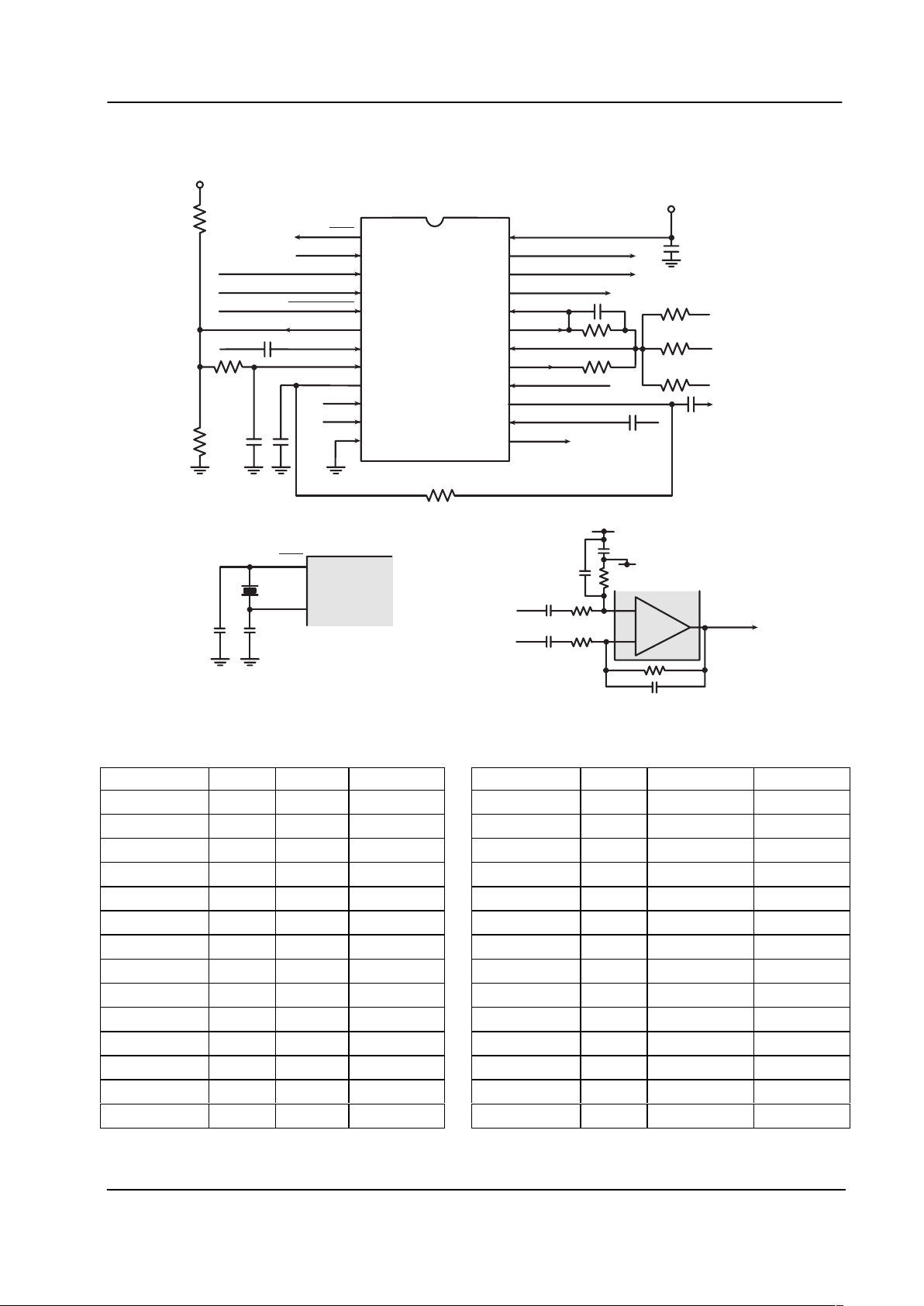
Figure 2: Recommended External Components
Component Notes Value Tolerance Component Notes Value Tolerance
R1
10k
±10% C2
.47F
±20%
R2
10k
±10% C3 270pF ±20%
R3
20k
±10% C4 270pF ±20%
R4
20k
±10% C5
0.1F
±20%
R5
10k
±10% C6 33pF ±20%
R6
2.2M
±10% C7 5-65pF ±20%
R7
100k
±10% C8
1.0F
±20%
R8
100k
±10% C9
1.0F
±20%
R9
100k
±10% C10
1.0F
±20%
R10
100k
±10% C11 22pF ±20%
R11
100k
±10% C12
0.1F
±20%
R12
2.2M
±10% C13
0.01F
±20%
R13
470k
±10% C14
0.01F
±20%
C1
.47F
±20% X1 4.00MHz
Table 2: Recommended External Components
Page 7

Audio Processor 7 MX806A
1998 MX-COM, Inc. www.mxcom.com Tel: 800 638 5577 336 744 5050 Fax: 336 744 5054 Doc. # 20480064.006
4800 Bethania Station Road, Winston-Salem, NC 27105-1201 USA All trademarks and service marks are held by their respective companies.
Recommended External Component Notes:
1. Input Op-Amp gain/attenuation components (voltage gain = 6.0dB) are shown in Inset 1 is a differential
configuration to demonstrate the versatility of this input. Components for a single (+ or -) input may be
used.
2. Resistor values R7 to R11 (summation components) are dependent upon application and configuration
requirements.
3. Xtal circuit capacitors C6 (CD) and C7 (CG) shown in Inset 2 are recommended in accordance with MXCOM’s Crystal Oscillator Application Note. Circuit drive and drain resistors are incorporated on-chip.
Operation of any MX-COM IC without a Xtal clock input may cause device damage. To minimize damage
in the event of a Xtal/drive failure, you should install a current limiting device (resistor or fast-reaction
fuse) on the power-input (V
DD
).
4 General Description
The MX806A LMR audio processor is intended too primarily to operate as the “Audio Terminal” or radio
systems using the DBS800 Digitally Integrated Baseband Subsystem.
The MX806A half-duplex device has signal paths and level setting elements that are configured and adjusted
by digital information sent from the radio microcontroller using C-BUS protocol. (C-BUS is the serial interface
for all DBS 800 ICs.)
4.1 Signal Path
The Signal path is divided into three sections:
Input Process:
This stage has selectable TX/RX paths. Transmits voice signals pass through microphone
pre-amplifier, voltage controlled gain (VOGAD) and highpass filter stages. Received audio is de-emphasized.
This initial audio, after line-in gain adjustment, may be switched to external audio processes (such as
scrambling) or to the internal Main Process stages.
Main Process
: Conditioning for the input or external process signals is completed in this stage. It is
comprised of pre-emphasis, high and lowpass switched capacitor filters and a deviation limiter.
Mixing and Output Drives
: Main audio for transmission is mix with signaling and data from external sources
(other DBS 800 ICs) to provide the composite signal for the digitally adjustable transmitter modulation drives.
Received audio level is adjusted for output to loudspeaker circuitry.
If selected, signal level stability and output accuracy of the MX806A is maintained by a voltage-controlled gain
system using selectable signal-level detectors. Signal levels can be dynamically controlled to provide
“dynamic compensation” for factors such as temperature drift, VCO non-linearity, etc.
The MX806A audio stages can be completely disabled – or the whole IC can be placed into powersave mode,
leaving only clock and C-BUS circuitry active.
4.2 VOGAD
The overall Gain Control system of the MX806A consists of 2 selectable signal peak detectors whose output
is fed via external integrating components to adjust the gain of the Voltage Controlled Amplifier positioned in
the TX Input Process Path. The transmit input signals is presented to Peak Detector 1 or 2. The Peak
Detectors are enabled individually by a Mode Command. When the input signal exceeds the peak - to - peak
threshold of the detector, a 5-volt level is produced at the VOGAD Out pin. This level remains for as long as
the signal exceeds the threshold. The integrated level to the VOGAD In pin causes the Voltage Controlled
Amplifier gain to be reduced. As can be seen from Figure 3 and Figure 5, Peak Detector 1 allows control of
the audio level to the external audio process and Peak Detector 2 allows control of transmit deviation levels.
Page 8

Audio Processor 8 MX806A
1998 MX-COM, Inc. www.mxcom.com Tel: 800 638 5577 336 744 5050 Fax: 336 744 5054 Doc. # 20480064.006
4800 Bethania Station Road, Winston-Salem, NC 27105-1201 USA All trademarks and service marks are held by their respective companies.
ä
-
+
MIC. IN
MIC. IN
MIC. OUT
VOGAD
(Voltage Controlled)
AMPLIFIER
TX INPUT PROCESS
MAIN PROCESS
RX
DRIVE
TX
TX
DRIVES
VOGAD
IN
VOGAD
OUT
EXTERNAL INTEGRATION COMPONENTS
HI - LO PEAK
DETECTOR
HI PEAK
DETECTOR
CAL
INPUT
V
V
DD
SS
R5
R6
R12
C8
To EXTERNAL AUDIO PROCESSES
PROCESSED AUDIO IN
Figure 3: VOGAD Sensors and Timing Components (from Figure 5)
VOGAD attack and decay times are set using the external components shown in Figure 2 and Figure 3. They
are calculated as described below.
4.2.1 VOGAD Components Calculations – Figure 2 and Figure 5
2
C8 x R6
)(T TimeDecay
C8 x R5 )(T Time Attack
Then
R5 R12 R6 and 1.0k R5 Provided
D
A
4.3 Calibration Methods
To effectively null all internal IC tolerance, the following initial calibration routine is suggested.
4.3.1 TX Calibration: From Mic. In to Modulator Drives Out
Disable Peak Detectors (Mode Command)
Set Transmitter Drives to 0dB (Mod. Levels Set)
Pre-emphasis may be employed as required (Control Command)
Set Input Level Amp to 0dB Control Command)
1. Mic. In = 250mVRMS at 1kHz. Set Process Gain Amp for output of 1440mV
P-P
(100% deviation).
2. With Process Gain Amp set as 1 and with Mic. In = 25mV
RMS
at 1kHz, set the Input Level Amp for an
output level of 308mV
RMS
(60% deviation)
4.3.2 RX Calibration: From RX Audio In to Audio Out
Set Audio Output Drive In to Audio Out
Leave Process Gain Amp set as 1 (See Section 4.3.1)
3. With and RX Audio In level of between 154mV
RMS
and 308mV
RMS
(See Section 7) at 1kHz, set the Input
Level Amp for and output level of 308mV
RMS
.
Page 9

Audio Processor 9 MX806A
1998 MX-COM, Inc. www.mxcom.com Tel: 800 638 5577 336 744 5050 Fax: 336 744 5054 Doc. # 20480064.006
4800 Bethania Station Road, Winston-Salem, NC 27105-1201 USA All trademarks and service marks are held by their respective companies.
RADIO
AND
CLUSTER
MICRO-
CONTROLLER
EXTERNAL DATA
PROM
DRAM
"C-BUS" SERIAL DATA SYSTEM
MX809
MX805A
MX803A
MX802
MX806A
Transmitter
MOD
VCO
REF.
L
MSK
MODEM
SUB-AUDIO
SIGNALING
PROCESSOR
AUDIO
SIGNALING
PROCESSOR
DAT A/VOICE
STORE AND
RETRIEVE
CODEC
RECEIVE
AND
TRANSMIT
AUDIO
PROCESSOR
AUDIO
Receiver
DEMOD
TX TONE AUDIO SIGNALS AND CUE
1200 BA UD MSK SIGNALS
TX SUB-AUDIO SIGNALS
RX (AUDIO, MSK, TONE, SUB-AUDIO) SIGNALS
4.032MHz XT AL
XTAL
XTAL XTAL
Figure 4 - MX806A Interfaced with Other DBS800 Elements
Figure 4: MX806A Interfaced with Other DBS 800 Elements
Page 10

Audio Processor 10 MX806A
1998 MX-COM, Inc. www.mxcom.com Tel: 800 638 5577 336 744 5050 Fax: 336 744 5054 Doc. # 20480064.006
4800 Bethania Station Road, Winston-Salem, NC 27105-1201 USA All trademarks and service marks are held by their respective companies.
➤
➤
➤
Figure 5: LMR Audio Processor Explanatory Block Diagram
5 Controlling Protocol
Control of the functions and levels within the MX806A LMR Audio processor is by a group of
Address/Commands and appended data instructions from the system microcontroller. The use of these
instructions is detailed in the following paragraphs and tables.
Command Assignment Address/Command Binary Command Data Table
HEX
MSB LSB
General Reset 01 00000001
Control Command 10 00010000 + 1 byte 2
Mode Command 11 00010001 + 1 byte 3
Mod. Levels Set 12 00010010 + 2 bytes 4
Volume Set 13 00010011 + 1 byte 5
Table 3: C-BUS Address/Commands
In “C-BUS” protocol the MX806A is allocated Address/Command values 10H and 13H. C-BUS Command
Mode, Modulation and Volume assignments, and data requirements are given in Table 3 and illustrated in
Figure 5.
Commands and Data are only to be loaded in the group configurations detailed since the “C-BUS” interface
recognizes the first byte after Chip Select (logic “0”) as an Address/Command.
Function or Level control data, which is detailed in Table 4, Table 5, Table 6, and Table 7, is acted upon at
the end of the loaded instruction
Page 11

Audio Processor 11 MX806A
1998 MX-COM, Inc. www.mxcom.com Tel: 800 638 5577 336 744 5050 Fax: 336 744 5054 Doc. # 20480064.006
4800 Bethania Station Road, Winston-Salem, NC 27105-1201 USA All trademarks and service marks are held by their respective companies.
Upon power-up the value of the “bits” in this device will be random (either “0” or “1”). A General Reset
Command (01H) is required. This command is provided to “reset” all devices on the Command “Data line and
has the following effect on the MX806A:
Control Address Command Loaded as 00
H
Mode Address Command Loaded as 00
H
Volume Set Loaded as 00
H
5.1.1 Control Command – (Preceded by A/C 10H)
Settings Control Bits
MSB
7 Audio Output (RX)
0
1
Disabled
Enabled
6 Modulation Drives
0
1
Disabled
Enabled
5 Pre-Emphasis
0
1
Bypass
Enabled
4 Input Select
0
1
RX In
Mic. In
3210 Input Level Set
0
0
0
0
0
0
0
0
1
1
1
1
1
1
1
1
0
0
0
0
1
1
1
1
0
0
0
0
1
1
1
1
0
0
1
1
0
0
1
1
0
0
1
1
0
0
1
1
0
1
0
1
0
1
0
1
0
1
0
1
0
1
0
1
Input Amp Disabled
–4.0dB
–3.0dB
–2.0dB
–1.0dB
0dB
1.0dB
2.0dB
3.0dB
4.0dB
5.0dB
6.0dB
7.0dB
8.0dB
9.0dB
10.0dB
Table 4: Control Commands
Page 12

Audio Processor 12 MX806A
1998 MX-COM, Inc. www.mxcom.com Tel: 800 638 5577 336 744 5050 Fax: 336 744 5054 Doc. # 20480064.006
4800 Bethania Station Road, Winston-Salem, NC 27105-1201 USA All trademarks and service marks are held by their respective companies.
5.1.2 Mode Command – (Preceded by A/C 11H)
Setting Mode Bits
MSB
7 Drive Source
0
1
Signals
Calibration
6 Deviation Limiter
0
1
Disabled
Enabled
5 VOGAD
0
1
Disabled
Enabled
4 De-Emphasis
0
1
Enabled
Bypassed
3 Signal Select
0
1
Internal
External
2 1 0 Process Gain Set
0
0
0
0
1
1
1
1
0
0
1
1
0
0
1
1
0
1
0
1
0
1
0
1
–4.0dB
–3.0dB
–2.0dB
–1.0dB
0dB
1.0dB
2.0dB
3.0dB
Table 5: Mode Commands
Page 13

Audio Processor 13 MX806A
1998 MX-COM, Inc. www.mxcom.com Tel: 800 638 5577 336 744 5050 Fax: 336 744 5054 Doc. # 20480064.006
4800 Bethania Station Road, Winston-Salem, NC 27105-1201 USA All trademarks and service marks are held by their respective companies.
5.1.3 Modulator Levels – (Preceded by A/C 12H)
Setting Modulator Drives
Byte 1 First byte for transmission
MSB
765
0 0 0 Must be “0”
43210 VCO Drive Attenuation
0
0
0
0
0
0
0
0
0
0
0
0
0
0
0
0
1
1
1
1
1
1
1
1
1
1
1
1
1
1
1
1
0
0
0
0
0
0
0
0
1
1
1
1
1
1
1
1
0
0
0
0
0
0
0
0
1
1
1
1
1
1
1
1
0
0
0
0
1
1
1
1
0
0
0
0
1
1
1
1
0
0
0
0
1
1
1
1
0
0
0
0
1
1
1
1
0
0
1
1
0
0
1
1
0
0
1
1
0
0
1
1
0
0
1
1
0
0
1
1
0
0
1
1
0
0
1
1
0
1
0
1
0
1
0
1
0
1
0
1
0
1
0
1
0
1
0
1
0
1
0
1
0
1
0
1
0
1
0
1
12.4dB
12.0dB
11.6dB
11.2dB
10.8dB
10.4dB
10.0dB
9.6dB
9.2dB
8.8dB
8.4dB
8.0dB
7.6dB
7.2dB
6.8dB
6.4dB
6.0dB
5.6dB
5.2dB
4.8dB
4.4dB
4.0dB
3.6dB
3.2dB
2.8dB
2.4dB
2.0dB
1.6dB
1.2dB
0.8dB
0.4dB
0dB
Page 14

Audio Processor 14 MX806A
1998 MX-COM, Inc. www.mxcom.com Tel: 800 638 5577 336 744 5050 Fax: 336 744 5054 Doc. # 20480064.006
4800 Bethania Station Road, Winston-Salem, NC 27105-1201 USA All trademarks and service marks are held by their respective companies.
Setting Modulator Drives
Byte 0 Last byte for transmission
MSB
765
0 0 0 Must be “0”
43210 VCO Drive Attenuation
0
0
0
0
0
0
0
0
0
0
0
0
0
0
0
0
1
1
1
1
1
1
1
1
1
1
1
1
1
1
1
1
0
0
0
0
0
0
0
0
1
1
1
1
1
1
1
1
0
0
0
0
0
0
0
0
1
1
1
1
1
1
1
1
0
0
0
0
1
1
1
1
0
0
0
0
1
1
1
1
0
0
0
0
1
1
1
1
0
0
0
0
1
1
1
1
0
0
1
1
0
0
1
1
0
0
1
1
0
0
1
1
0
0
1
1
0
0
1
1
0
0
1
1
0
0
1
1
0
1
0
1
0
1
0
1
0
1
0
1
0
1
0
1
0
1
0
1
0
1
0
1
0
1
0
1
0
1
0
1
6.2dB
6.0dB
5.8dB
5.6dB
5.4dB
5.2dB
5.0dB
4.8dB
4.6dB
4.4dB
4.2dB
4.0dB
3.8dB
3.6dB
3.4dB
3.2dB
3.0dB
2.8dB
2.6dB
2.4dB
2.2dB
2.0dB
1.8dB
1.6dB
1.4dB
1.2dB
1.0dB
0.8dB
0.6dB
0.4dB
0.2dB
0dB
Table 6: Modulator Drive Levels
Page 15

Audio Processor 15 MX806A
1998 MX-COM, Inc. www.mxcom.com Tel: 800 638 5577 336 744 5050 Fax: 336 744 5054 Doc. # 20480064.006
4800 Bethania Station Road, Winston-Salem, NC 27105-1201 USA All trademarks and service marks are held by their respective companies.
5.1.4 Volume Set – (Preceded by A/C 13H)
Setting Volume Set
MSB
7 5 Main Process Out
0
0
0
1
Enabled
Biased
5 Powersave
0
1
Chip Enabled
Powersaved
43210 VCO Drive Attenuation
0
0
0
0
0
0
0
0
0
0
0
0
0
0
0
0
1
1
1
1
1
1
1
1
1
1
1
1
1
1
1
1
0
0
0
0
0
0
0
0
1
1
1
1
1
1
1
1
0
0
0
0
0
0
0
0
1
1
1
1
1
1
1
1
0
0
0
0
1
1
1
1
0
0
0
0
1
1
1
1
0
0
0
0
1
1
1
1
0
0
0
0
1
1
1
1
0
0
1
1
0
0
1
1
0
0
1
1
0
0
1
1
0
0
1
1
0
0
1
1
0
0
1
1
0
0
1
1
0
1
0
1
0
1
0
1
0
1
0
1
0
1
0
1
0
1
0
1
0
1
0
1
0
1
0
1
0
1
0
1
OFF
48.0dB
46.4dB
44.8dB
43.2dB
41.6dB
40.0dB
38.4dB
36.8dB
35.2dB
33.6dB
32.0dB
30.4dB
28.8dB
27.2dB
25.6dB
24.0dB
22.4dB
20.8dB
19.2dB
17.6dB
16.0dB
14.4dB
12.8dB
11.2dB
9.6dB
8.0dB
6.4dB
4.8dB
3.2dB
1.6dB
0dB
Table 7: Volume Set
Notes:
1. Command Loading: Address/Commands and data bytes must be loaded in accordance with the
information given in Figure 7.
2. The powersave function is enabled by bit 5 of the Volume Set Command (Table 7).
During Powersave all internal elements except the clock Generator and “C-BUS” interface are off. The
Mic Op-Amp and output Drive stage outputs are connected to V
SS
.
3. Modulator Drives are controlled separately, but the whole two-byte modulator Drive command must be
loaded for each requirement adjustment.
4.
Select Chip must be held at a logic “1” for the period “t
CSOFF
” between transactions.
Page 16

Audio Processor 16 MX806A
1998 MX-COM, Inc. www.mxcom.com Tel: 800 638 5577 336 744 5050 Fax: 336 744 5054 Doc. # 20480064.006
4800 Bethania Station Road, Winston-Salem, NC 27105-1201 USA All trademarks and service marks are held by their respective companies.
6 Application Notes
To assist in rapid setting, this quick-reference list should be used with Figure 5.
Control A/C = 10
H
7 Audio Out (RX) Enable
6 Modulator Drive Enable
5 Pre-Emphasis Select
4 Input Select (RX/TX)
3-0 Input Level Set (-4dB to 10dB)
Mode A/C = 11
H
7 Drive Source
6 Derivation Limiter Enable
5 VOGAD Enable
4 De-emphasis Enable
3 Signal Select
2-0 Process Gain Set
Modulator Levels A/C = 12
H
Byte 1
7-5 “0”
4-0 Mod 1 Attenuation (0 to 12.4dB)
Byte 2
7-5 “0”
4-0 Mod 2 Attenuation (0 to 6.2dB)
Volume Set A/C = 13
H
7-6 “0”
5 Powersave
4-0 Volume Set Attenuation (0 to 48dB)
Table 8: Quick Reference List
GENERAL RESET
MSB LSB
Sets the Control, Mode and Volume Commands to 00
H
7
6
5
4
3
21
0
MSB LSB
CONTROL COMMAND 1 DAT A BYTE
MSB LSB
MODE COMMAND 1 DATA BYTE
MSB LSB
VOLUME SET 1 DATA BYTE
MSB LSB
MODULAT OR LEVELS SET
2 DATA BYTES - BYTE 1 (loaded first) BYTE 0 (loaded last)
TABLE 4
TABLE 5
TABLE 3
TABLE 2
7
6
5
4
3
21
0
7
6
5
4
3
21
0
7
6
5
4
3
21
0
7
6
5
4321
0
Figure 6: Examples of Command Data Configurations
Page 17

Audio Processor 17 MX806A
1998 MX-COM, Inc. www.mxcom.com Tel: 800 638 5577 336 744 5050 Fax: 336 744 5054 Doc. # 20480064.006
4800 Bethania Station Road, Winston-Salem, NC 27105-1201 USA All trademarks and service marks are held by their respective companies.
7 Performance Specifications
7.1 Electrical Specifications
7.1.1 Absolute Maximum Limits
Exceeding these maximum ratings can result in damage to the device.
General Notes Min. Typ. Max. Units
Supply (VDD-VSS) -0.3 7.0 V
Voltage on any pin to V
SS
-0.3 VDD + 0.3 V
Current
V
DD
-30 30 mA
V
SS
-30 30 mA
Any other pin -20 20 mA
P / DW / LH Packages
Total allowable Power dissipation
at T
AMB
= 25C
800 mW
Derating above 25C
10
mW/C above 25C
Operating Temperature -40 85
C
Storage Temperature -55 125
C
Table 9: Absolute Maximum Ratings
7.1.2 Operating Limits
Correct Operation of the device outside these limits is not implied.
Notes Min. Typ. Max. Units
Supply (VDD-VSS) 4.5 5.0 5.5 V
Operating Temperature -40 85
C
Xtal Frequency 4.0 MHz
Table 10: Operating Limits
Page 18

Audio Processor 18 MX806A
1998 MX-COM, Inc. www.mxcom.com Tel: 800 638 5577 336 744 5050 Fax: 336 744 5054 Doc. # 20480064.006
4800 Bethania Station Road, Winston-Salem, NC 27105-1201 USA All trademarks and service marks are held by their respective companies.
7.1.3 Operating Characteristics
For the following conditions unless otherwise specified.
V
DD
= 5.0V @ T
AMB
= 25C
Xtal/Clock Frequency = 4.0MHz, Audio Level 0dB ref. = 308mV
RMS
@ 1kHz (60% deviation, FM)
Notes Min. Typ. Max. Units
Static Values
Supply Current
All Elements Enabled 8.0 15.0 mA
Maximum Powersave 0.7 1.5 mA
“C-BUS” Interface
Input Logic “1” 3.5 V
Input Logic “0” 1.5 V
Input Current -1.0 1.0
A
Input Capacitance 7.5 pF
Overall Performance
Microphone Input Level 1, 2 25 mV
RMS
Discriminator Input Level 2, 3 154 308 mV
RMS
Output Drive Level
60% Deviation 2, 4 291 308 326 mV
RMS
100% Deviation 2, 4, 5 1440 MV
P-P
Passband 6 297 3000 Hz
Passband Ripple 7 -2 0.5 dB
Stopband Attenuation 6, 8
@ 150Hz 10 12 dB
@ 3400Hz 2 dB
@ 6000Hz 30 36 dB
@ 8000Hz to 20,000Hz 60 dB
Signal Path Noise
TX -50 dBp
TX 9 -45 dB
RX -60 dB
RX 9 -55 dB
Total Harmonic Distortion
RX or TX, 60% Deviation 1.0 %
Circuit Elements – Figure 5
Mic. Amp or Mod. Summation Amp
Open Loop Gain 50.0 dB
Bandwidth 20.0 kHz
Input Impedance 10.0
M
Output Impedance
Open Loop 6.0
k
Closed Loop 600
De-emphasis
Slope -6.0 dB/octave
Gain 0 dB
Input Impedance 1
M
Page 19

Audio Processor 19 MX806A
1998 MX-COM, Inc. www.mxcom.com Tel: 800 638 5577 336 744 5050 Fax: 336 744 5054 Doc. # 20480064.006
4800 Bethania Station Road, Winston-Salem, NC 27105-1201 USA All trademarks and service marks are held by their respective companies.
Notes Min. Typ. Max. Units
Voltage Controlled Gain Amp (VOGAD)
Gain
Non-Compression 2 6.0 dB
Full-Compression -24 dB
Input Impedance 10.0
M
VOGAD Peak Detectors
Output Impedance
Logic “1” (Compress) 1
k
Logic “0” 10
M
Hi/Lo Peak Detector Threshold 10 1300 mV
P-P
Hi Peak Detector Threshold 10 650 mV + ve pk
Input (Low + Highpass) Filter
Gain @ 1.0kHz -1.0 1.0 dB
Input Level Amp
Gain Range 0 dB
Overall Tolerance -1.0 1.0 dB
Step Size 0.75 1.0 1.25 dB
External Audio Buffer
Gain -0.1 0 0.1 dB
Pre-emphasis (Main Process and VOGAD)
Slope 6.0 dB/octave
Gain @ 1.0kHz 10.0 dB
Process Highpass Filter
Gain @ 1.0kHz -0.1 0 0.1 dB
Deviation Limiter
Threshold 708 1300 1413 mV
RMS
Gain -0.5 0.5 dB
Process Lowpass Filter
Gain @ 1.0kHz -0.1 0 0.1 dB
Process Gain Amp
Gain Range -4.0 3.0 dB
Overall Tolerance -0.5 0.5 dB
Step Size 0.75 1.0 1.25 dB
Output Impedance 600
Transmitter Modulator Drives
Input Impedance 15.0
k
Mod. 1 Attenuator
Attenuation Range 0 12.4 dB
Overall Tolerance -1 1 dB
Step Size 0.2 0.4 0.6 dB
Output Impedance 600
Mod. 2 Attenuator
Attenuation Range 0 6.2 dB
Overall Tolerance -0.5 0.5 dB
Step Size 0.1 0.2 0.3 dB
Output Impedance 600
Page 20

Audio Processor 20 MX806A
1998 MX-COM, Inc. www.mxcom.com Tel: 800 638 5577 336 744 5050 Fax: 336 744 5054 Doc. # 20480064.006
4800 Bethania Station Road, Winston-Salem, NC 27105-1201 USA All trademarks and service marks are held by their respective companies.
Notes Min. Typ. Max. Units
Audio Output Attenuator
Attenuation Range 0 48.0 dB
Overall Tolerance -1.0 1.0 dB
Step Size 1.1 1.6 2.1 dB
Output Impedance 600
Miscellaneous Impedances
Processed Audio Input 500
k
Calibration Input 500
k
External Process Out 100
RX with De-emphasis Bypass 25.0
k
Table 11: Operating Characteristics
Operating Characteristics Notes:
1. Producing an output of 0dB with the Mic. Op-Amp set to 6dB (as shown in Figure 2) and the Modulator
Drives set to 0dB.
2. With Output Drives set to 0dB and the system calibrated as described in the Application Notes.
3. Input level range for 0dB output, by adjustment of the Input Level Amp.
4. It is recommended that these output levels will produce 60% or 100% deviation in the transmitter.
5. With the microphone input level 20dB above the level required to produce 0dB at the Output Drives.
6. Between Microphone or RX inputs to Modulator or Audio Outputs.
7. Deviation from the ideal overall response including the pre- or de-emphasis slope.
8. Excluding the effect of pre- or de-emphasis slope.
9. In a 30kHz bandwidth.
10. Using pre-emphasis in the TX path.
Page 21

Audio Processor 21 MX806A
1998 MX-COM, Inc. www.mxcom.com Tel: 800 638 5577 336 744 5050 Fax: 336 744 5054 Doc. # 20480064.006
4800 Bethania Station Road, Winston-Salem, NC 27105-1201 USA All trademarks and service marks are held by their respective companies.
7.1.4 Timing
Timing Parameters for two-way communications between the C and the MX805A on the C-BUS are shown
in Table 12.
C-BUS Timing Min. Typ. Max. Units
t
CSE
Chip Select Low to First Serial Clock Rising Edge 2.0
s
t
CHS
Last Serial Clock Rising Edge to Chip Select High 4.0
s
t
CSOFF
Chip Select High time between transactions 2.0
s
t
NXT
Inter-Byte Time 4.0
s
t
CK
Serial Clock Period 2.0
s
Table 12: Timing Information
Notes:
1. Command Data is transmitted to the peripheral MSB (bit 7) first, LSB (bit 0) last. Reply Data is read from
the MX805A MXB (bit 7) first, LSB (bit 0) last.
2. Data is clocked into the MX805A and into the microcontroller on the rising Serial Clock edge.
3. Loaded data instructions are acted upon at the end of each individual, loaded byte.
4. To allow for differing microcontroller serial interface formats, the MX806A will work with either polarity
Serial Clock pulses.
CHIP SELECT
SERIAL CLOCK
COMMAND DATA
ADDRESS/COMMAND
BYTE
LAST DATA BYTE
Logic level is not important
MSB LSB
t
t
CSOFF
t
CSH
t
NXT
t
NXT
CK
t
CSE
FIRST DATA BYTE
5432 0617543206175432 0617
Figure 7: C-BUS Timing Information
Page 22

Audio Processor 22 MX806A
1998 MX-COM, Inc. www.mxcom.com Tel: 800 638 5577 336 744 5050 Fax: 336 744 5054 Doc. # 20480064.006
4800 Bethania Station Road, Winston-Salem, NC 27105-1201 USA All trademarks and service marks are held by their respective companies.
7.2 Packages
NOTE: All dimensions in inches (mm.)
Angles are in degrees
PackageTolerances
A
B
C
E
E1
H
TYP. MAX.MIN.DIM.
J
J1
P
Y
T
K
L
0.220 (5.59)
0.555 (14.04)
0.670 (17.02)
7°
0.160 (4.05)
1.270 (32.26)
0.151 (3.84)
0.100 (2.54)
0.121 (3.07)
0.600 (15.24)
0.590 (14.99) 0.625 (15.88)
0.015 (0.38) 0.045 (1.14)
0.008 (0.20) 0.015 (0.38)
0.015 (0.38) 0.023 (0.58)
0.040 (1.02) 0.065 (1.65)
0.066 (1.67) 0.074 (1.88)
1.200 (30.48)
0.500 (12.70)
H
K
L
J1
J1
J
J
P
P
C
C
B
B
A
A
PIN1
PIN1
T
T
E
E
E1
E1
Y
Figure 8: 24-pin PDIP Mechanical Outline:
Order as part no. MX806AP
0.597 (15.16)
PackageTolerances
A
B
C
E
H
TYP. MAX.MIN.DIM.
J
P
X
W
T
Y
K
L
0.105 (2.67)
0.093 (2.36)
0.419 (10.64)
45°
7°
0°
10°
0.050 (1.27)
0.046 (1.17)
0.613 (15.57)
0.299 (7.59)
0.050 (1.27)
0.016 (0.41)
0.390 (9.90)
0.020 (0.51)0.003 (0.08)
0.009 (0.23)
0.0125 (0.32)
0.013 (0.33)
0.020 (0.51)
0.036 (0.91)
0.286 (7.26)
Z
NOTE: All dimensions in inches (mm.)
Angles are in degrees
5°
5°
PIN 1
A
B
X
P
J
Y
C
H
K
E
L
T
W
Z
Alternative Pin
Location
Marking
Figure 9: 24-pin SOIC Mechanical Outline:
Order as part no. MX806ADW
Page 23

Audio Processor 23 MX806A
1998 MX-COM, Inc. www.mxcom.com Tel: 800 638 5577 336 744 5050 Fax: 336 744 5054 Doc. # 20480064.006
4800 Bethania Station Road, Winston-Salem, NC 27105-1201 USA All trademarks and service marks are held by their respective companies.
PackageTolerances
NOTE: All dimensions in inches (mm.)
Angles are in degrees
A
B
C
D
E
H
P
F
G
TYP. MAX.MIN.DIM.
K
J
W
T
Y
0.435 (11.05)
0.435 (11.05)
0.051 (1.30)
0.009 (0.22)
6°
30°
0.409 (10.40)
0.409 (10.40)
0.146 (3.70)
0.417 (10.60)
0.417 (10.60)
0.049 (1.24)
0.006 (0.152)
0.250 (6.35)
0.250 (6.35)
0.023 (0.58)
0.047 (1.19)
0.022 (0.55)0.018 (0.45)
0.380 (9.61)
0.380 (9.61)
0.128 (3.25)
0.048 (1.22)
45°
F
G
P
A
D
B
E
PIN 1
W
C
J
K
Y
W
H
T
Figure 10: 24-pin PLCC Mechanical Outline:
Order as part no. MX806ALH
 Loading...