

Page 1

DATA BULLETIN
MX805A
1998 MX-COM, Inc. www.mxcom.com Tel: 800 638 5577 336 744 5050 Fax: 336 744 5054 Doc. # 20480116.004
4800 Bethania Station Road, Winston-Salem, NC 27105-1201 USA All trademarks and service marks are held by their respective companies.
Sub-Audio Signaling
Processor
Features
Non-predictive CTCSS Tone Decoder
DCS Sub-Audio Signal demodulator
CTCSS /NRZ Encoder with TX level
adjustment and lowpass filter output
stage with optional NRZ pre-emphasis
Selectable Sub-Audio bandstop filter
NoTone (CTCSS RX) period timer
Low Power Operation
Member of DBS800 Family (C-BUS
Compatible)
RX SUB-AUDIO
IN
RX LPF
RX AMP
AMP IN
AMP OUT
RX SUB-AUDIO
OUT
COMPARATOR
AMP
COMPARATOR
NRZ RX
DATA AND
BAUD RATE
EXTRACTOR
+
+
_
_
DIGITAL
NOISE
FILTER
FREQUENCY
ASSESMENT
NOTONE
TIMER
FREQUENCY
MEASUREMENT
C-BUS
INTERFACE
AND
CONTROL
LOGIC
TX LEVEL
ADJUST
NOTONE
COMMAND DA TA
REPLY DATA
INTERRUPT
SERIAL CLOCK
WAKE
ADDRESS SELECT
TX SUB-AUDIO
OUT
TX SUB-AUDIO LPF
AUDIO OUT
AUDIO BYPASS
CLOCK
GENERAT OR
AUDIO IN
XTAL/
CLOCK
XTAL
IN
OUT
V
DD
V
SS
V
BIAS
NRZ
TX DAT A
NRZ RX
BAUD RATE
NRZ
RX DATA
CTCSS SUB-
AUDIO FREQUENCY
CHIP SELECT
RAW NRZ DATA
RX
TX
SUB-AUDIO BANDSTOP
AUDIO SIGNAL PATH
VARIABLE
BANDWIDTH
180Hz/260Hz
DATA BUFFER
AND
SHIFT REGISTER
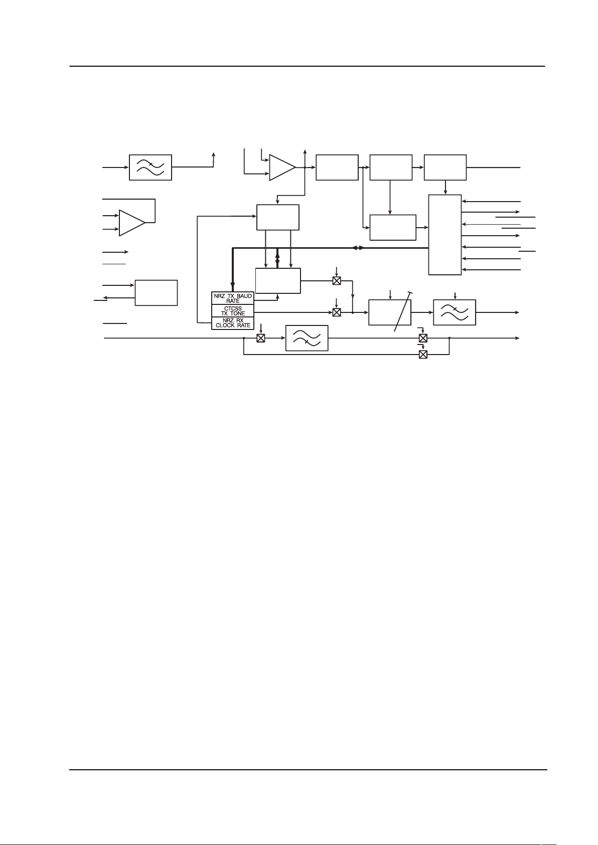
The MX805A is a sub-audio frequency signaling processor that provides outband audio and digital signaling
capability for LMR systems. Designed for the transmission and non-predictive reception of Continuous Tone
Controlled Squelch (CTCSS) tones and other non-standard frequencies, the MX805A also handles NonReturn-to Zero (NRZ) data reception and transmission to provide Digitally Coded Squelch (DCS/DPL
TM
) and
LTR
TM
signaling.
Setting the MX805A functions and modes is accomplished by data loaded from the microcontroller to the
controlling registers within the device. Reply Data and Interrupt protocol keep the microcontroller up to date
on the operational status of the circuitry. CTCSS tone data for transmission is generated in the
microcontroller, loaded to the CTCSS TX Frequency Register, encoded and output as a tone via the TX Subaudio LPF. Received non-predicted CTCSS tone frequencies are measured and the resulting data, in the
form of a 2-byte data word, is presented to the microcontroller for matching against a lookup table. Noise
filtering is provided to improve the signal quality prior to measurement. NRZ coded data streams for
transmission, when generated within a microcontroller, are loaded to the NRZ TX Data Buffer and output, in
8-bit bytes, through the lowpass filter circuitry as subaudible signals. DCS turnoff tones can be added to the
data signals by switching the MX805A to the CTCSS transmit mode at the appropriate time. NRZ coding is
produced by the microcontroller and translated to subaudio signals by the MX805A. Received NRZ data is
filtered, detected, and placed into the NRZ Data Register, which is then available for transfer (one byte at a
time) to the microcontroller for decoding by software. Clock extraction circuitry is provided on-chip. TX ad RX
baud rates are selectable.
Hardware and software are designed to allow consecutive addressing of two MX805A Sub-Audio Signaling
Processors to achieve multi-mode duplex operation. Powersaving may be controlled by software or by an
input dedicated to the purpose.
The MX805A may be used with a 5.0V power supply and is available in the following packages:
24-pin SOIC (MX805ADW), 24-pin PLCC (MX805ALH), and 24-pin PDIP (MX805AP).
Page 2

Sub-Audio Signaling Processor 2 MX805A
1998 MX-COM, Inc. www.mxcom.com Tel: 800 638 5577 336 744 5050 Fax: 336 744 5054 Doc. # 20480116.004
4800 Bethania Station Road, Winston-Salem, NC 27105-1201 USA All trademarks and service marks are held by their respective companies.
Contents
Section Page
1 Block Diagram................................................................................................................4
2 Signal List.......................................................................................................................5
3 External Components....................................................................................................7
3.1 Input configurations ............................................................................................................. 8
3.1.1 Using and External Op-Amp.....................................................................................................8
4 General Description.......................................................................................................9
4.1 Glossary .............................................................................................................................. 9
4.2 Operating Modes................................................................................................................. 9
4.2.1 NRZ Encoding...........................................................................................................................9
4.2.2 CTCSS Encoding......................................................................................................................9
4.2.3 NRZ Decoding ........................................................................................................................10
4.2.4 CTCSS Decoding....................................................................................................................10
5 Controlling Protocol....................................................................................................10
5.1 MX805A Internal Registers................................................................................................ 10
5.1.1 Control Register (70H/78H) ....................................................................................................10
5.1.2 Status Register (71H/79H)......................................................................................................10
5.1.3 CTCSS Rx Frequency Register (72H/7AH)............................................................................10
5.1.4 CTCSS Tx Frequency/NRZ Tx or Rx Baud Rate Register (73H/7BH) ...................................10
5.1.5 NRZ Rx Data Register (74H/7CH)..........................................................................................10
5.1.6 NRZ Tx Data Register (75H/7DH) ..........................................................................................10
5.1.7 Gain Set Register (76H/7EH)..................................................................................................10
5.2 Address/Commands.......................................................................................................... 11
5.2.1 Write to Control Register - A/C 70H (78H) followed by 1 byte of Command Data..................12
5.2.2 General Reset.........................................................................................................................12
5.2.3 Read Status Register –A/C 71H (79H) followed by 1 byte of Rely Data.................................13
5.2.4 Read CTCSS RX Frequency Register –A/C 72H (7AH) followed by 2 bytes of Reply Data ..13
5.2.5 Write to CTCSS TX Frequency/NRZ Baud Data Rate Register –A/C 73H (7BH) followed
by 2 bytes of Command Data. ................................................................................................15
5.2.6 Read NRZ RX Data Register – A/C 74H (7CH) followed by 1 byte Reply Data.....................17
5.2.7 Write to NRZ TX Data Register – A/C 75H (7DH) followed by 1 byte of Command Data. .....17
5.2.8 Write to Gain Set Register – A/C 76H (7EH) followed by 1 byte of Command Data..............17
Page 3

Sub-Audio Signaling Processor 3 MX805A
1998 MX-COM, Inc. www.mxcom.com Tel: 800 638 5577 336 744 5050 Fax: 336 744 5054 Doc. # 20480116.004
4800 Bethania Station Road, Winston-Salem, NC 27105-1201 USA All trademarks and service marks are held by their respective companies.
6 Performance Specifications........................................................................................18
6.1 Electrical Specifications..................................................................................................... 18
6.1.1 Absolute Maximum Limits..............................................................................................................18
6.1.2 Operating Limits ............................................................................................................................18
6.1.3 Operating Characteristics..............................................................................................................19
6.1.4 Timing............................................................................................................................................22
6.2 Packages........................................................................................................................... 23
MXCOM, Inc. reserves the right to change specifications at any time without notice.
Page 4
Sub-Audio Signaling Processor 4 MX805A
1998 MX-COM, Inc. www.mxcom.com Tel: 800 638 5577 336 744 5050 Fax: 336 744 5054 Doc. # 20480116.004
4800 Bethania Station Road, Winston-Salem, NC 27105-1201 USA All trademarks and service marks are held by their respective companies.
1 Block Diagram
RX SUB-AUDIO
IN
RX LPF
RX AMP
AMP IN
AMP OUT
RX SUB-AUDIO
OUT
COMPARATOR
AMP
COMPARATOR
NRZ RX
DATA AND
BAUD RATE
EXTRACTOR
+
+
_
_
DIGITAL
NOISE
FILTER
FREQUENCY
ASSESMENT
NOTONE
TIMER
FREQUENCY
MEASUREMENT
C-BUS
INTERFACE
AND
CONTROL
LOGIC
TX LEVEL
ADJUST
NOTONE
COMMAND DATA
REPL Y DAT A
INTERRUPT
SERIAL CLOCK
WAKE
ADDRESS SELECT
TX SUB-AUDIO
OUT
TX SUB-AUDIO LPF
AUDIO OUT
AUDIO BYPASS
CLOCK
GENERAT OR
AUDIO IN
XTAL/
CLOCK
XTAL
IN
OUT
V
DD
V
SS
V
BIAS
NRZ
TX DATA
NRZ RX
BAUD RATE
NRZ
RX DATA
CTCSS SUB-
AUDIO FREQUENCY
CHIP SELECT
RAW NRZ DATA
RX
TX
SUB-AUDIO BANDSTOP
AUDIO SIGNAL PATH
VARIABLE
BANDWIDTH
180Hz/260Hz
DATA BUFFER
AND
SHIFT REGISTER
Figure 1: Block Diagram
Page 5
Sub-Audio Signaling Processor 5 MX805A
1998 MX-COM, Inc. www.mxcom.com Tel: 800 638 5577 336 744 5050 Fax: 336 744 5054 Doc. # 20480116.004
4800 Bethania Station Road, Winston-Salem, NC 27105-1201 USA All trademarks and service marks are held by their respective companies.
2 Signal List
Pin Signal Description
1
Xtal
The output from the on-chip clock oscillator inverter. External components are
required at this input when a Xtal input is used. See Figure 2.
2 Xtal/Clock
The input to the clock oscillator inverter. A Xtal or externally derived clock should
be connected here.
3 Address Select This input enables two MX805A’s to be used on the same C-BUS to provide dull-
duplex operation. See Table 4 and Table 5.
4
IRQ Request Interrupt . The output of this pin indicates an interrupt condition to the
microcontroller by going to a logic ‘0”. This ‘wire-or-able’ output allows the
connection of up to 8 peripherals to 1 interrupt port on the microcontroller. This
pin has a low impedance pulldown to logic ‘0’ when active, and a high impedance
when inactive. The system
IRQ line requires 1 pull-up resistor to VDD. The
conditions that cause interrupts are indicated in the Table 5 and Table 7.
5 Serial Clock
This is the ‘C-BUS’ serial Clock input. This clock, produced by the
microcontroller, is used for transfer timing of commands and data to and from the
MX805A. See timing diagrams.
6 Command Data This is the ‘C-BUS’ serial data input from the microcontroller. Data is loaded to
this device in 8-bit bytes, MSB (bit 7) first and LSB (bit 0) last, synchronized to the
Serial Clock. See Timing diagrams.
7
CS
Select Chip . This is the ‘C-BUS’ data loading control function. This input is
provided by the microcontroller. Data transfer sequences are initiated, completed
or aborted by the
CS signal. See Timing diagrams.
8 Reply Data This is the ‘C-BUS’ serial data output to the microcontroller. The transmission of
Reply Data bytes is synchronized to the Serial Clock under the control of the
CS
input. This 3-state output is held at high impedance when not sending data to the
microcontroller. See Timing Diagrams
9 TX Sub-Audio Out This is the subaudio output (pure or NRZ derived). Signals are band limited. The
TX Output Filter had a variable bandwidth (See Table 9). This output is at V
BIAS
(a) when the NRZ Encoder is enabled but no data is being transmitted, (b) when
the MX805A is placed in the Powersave All condition.
10 Audio In This is the input to the switched sub-audio bandstop (highpass) filter. It is
internally biased, and should be AC coupled by capacitor C7.
11 Audio Out This is the output of the audio signal path (filter or bandpass). It is controlled by
the Control Register. When disabled, the pin is held at V
BIAS
.
12 V
SS
Negative Supply (GND)
13 RX Amp In (-)
This is the inverting input to the on-chip RX Input Amp. (See Figure 2, Figure 3,
and Figure 4).
14 RX Amp In (+) This is the non-inverting input to the on-chip RX Input Amp.
15 RX Amp Out This is the output of the on-chip RX Input Op-Amp. This circuit may be used, with
external components, as a signal amplifier and anti-aliasing filter prior to the RX
Lowpass Filter, or for other purposes. See Figure 2 for Component details.
16 RX Sub-Audio In This is the received Sub-Audio (CTCSS/NRZ) input. It is internally referenced to
V
BIAS
. This signal to this pin should be AC coupled or biased. See Figure 2.
17 RX Sub-Audio Out
This is the output of the RX lowpass filter. It may be coupled into the on-chip
amplifier or comparator as required.
18 V
BIAS
The internal circuitry bias line, held at VDD/2. This pin must be decoupled to V
SS
by capacitor C8. See Figure 2.
19 Comparator In (-) This is the inverting input to the on-chip ‘comparator’ amplifier. See Figure 2,
Figure 3, and Figure 4.
20 Comparator In (+)
This is the non-inverting input to the on-chip ‘comparator’ amplifier. See Figure 2,
Figure 3, and Figure 4.
Page 6
Sub-Audio Signaling Processor 6 MX805A
1998 MX-COM, Inc. www.mxcom.com Tel: 800 638 5577 336 744 5050 Fax: 336 744 5054 Doc. # 20480116.004
4800 Bethania Station Road, Winston-Salem, NC 27105-1201 USA All trademarks and service marks are held by their respective companies.
Pin Signal Description
21 Comparator Out
This is the output of the ‘comparator’ amplifier. This node is also connected
internally to the input of the /digital Noise Filter (See Figure 1). When both
decoders (CTCSS or NRZ) are powersaved, this output is at a logic ‘0’.
22 Notone Timing External RC components connected to this pin form the timing mechanism of a
Notone period timer. The external network determines the “charge rate” of the
timer to V
BIAS
. The expiration of the timer will cause an interrupt. This function is
only used in the CTCSS RX mode. See page 9.
23
Wake
This ‘real time’ input can be used to reactivate the MX805A from the ‘Powersave
All’ condition using an externally derived signal. The MX805A will be in
‘Powersave All’ condition when both this pin and bit 0 of the Control Register are
set to a logic ‘1’. Recovery from ‘Powersave All’ is achieved by putting either the
Wake
pin or the ‘Powersave All” bit at logic ‘0’. This allows MX805A activation by
the microcontroller or an external signal, such as RSSI or Carrier Detect.
24 V
DD
Positive Supply. A single 5.0V regulated supply is required.
Note: More information on external components and the DBS800 system integration of the MX805A are
contained in the DBS800 System Support Documentation. Guidance on the generation and
manipulation of NRZ and RX and TX data is given in the DBS800 Application support documentation.
C-BUS: This is MX-COM’s proprietary standard for the transmission of commands and data between a
microcontroller and DBS8000 microcircuits. It may be used with any microcontroller, and can, if
desired, take advantage of the hardware and serial I/O functions embodied into many types of
microcontroller. The C-BUS data rate is determined by the microcontroller.
Table 1: Signal List
RX CTCSS Tone Measurement Completed
CTCSS NOTONE Timer Expired
1 NRZ RX Data Byte Received
New NRZ Data Received Before Last Byte Read
NRZ TX Buffer Ready
NRZ Data Transmission Complete
Table 2: Interrupt Conditions
Page 7
Sub-Audio Signaling Processor 7 MX805A
1998 MX-COM, Inc. www.mxcom.com Tel: 800 638 5577 336 744 5050 Fax: 336 744 5054 Doc. # 20480116.004
4800 Bethania Station Road, Winston-Salem, NC 27105-1201 USA All trademarks and service marks are held by their respective companies.
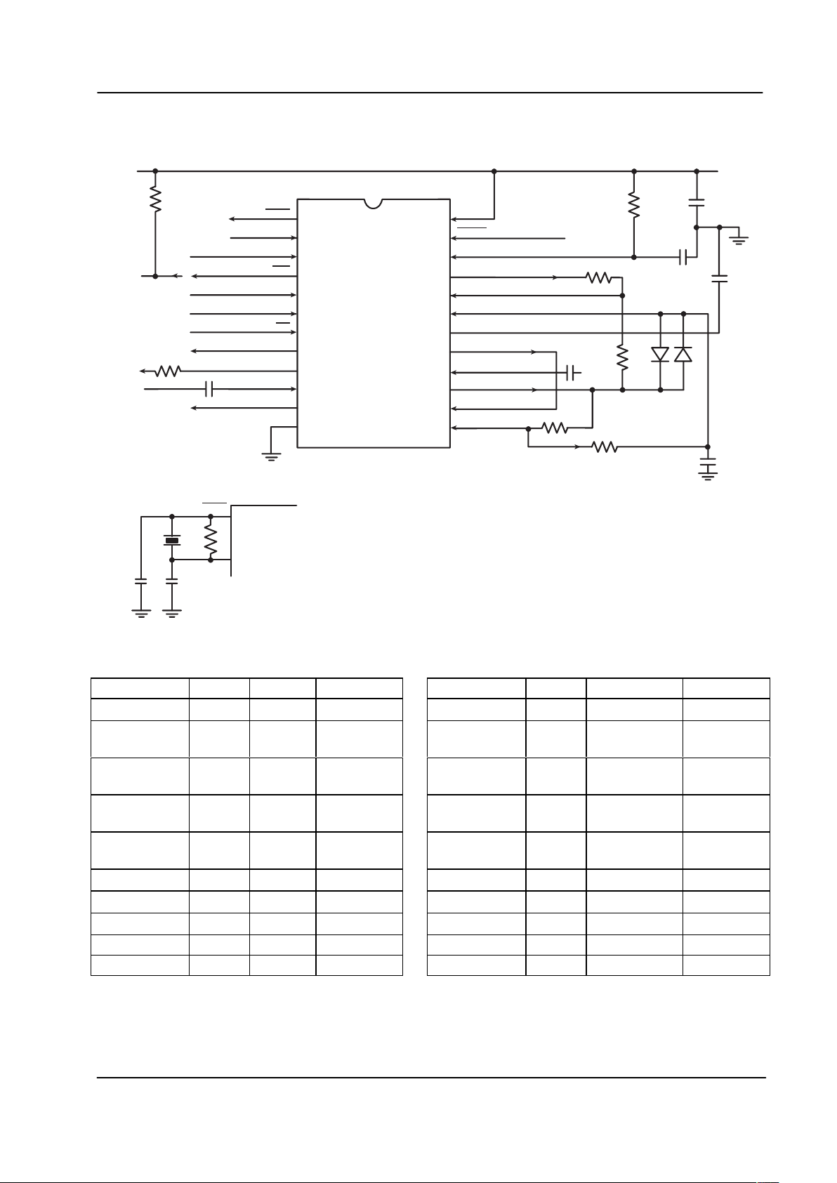
3 External Components
1
2
3
4
5
6
7
8
9
10
11
12
24
23
22
21
20
19
18
17
16
15
14
13
MX805AJ
XTAL
IRQ
CS
XTAL/CLOCK
ADDRESS SELECT
SERIAL CLOCK
COMMAND DAT A
REPL Y DA TA
TX SUB-AUDIO OUT
AUDIO IN
AUDIO OUT
BIAS
V
V
SS
V
DD
DD
WAKE
NOTONE
COMP ARATOR OUT
COMP ARATOR IN (+)
COMP ARATOR IN (-)
V
RX SUB-AUDIO OUT
RX SUB-AUDIO IN
RX AMP OUT
RX AMP IN (+)
RX AMP IN (-)
SEE INSET
C7
R8
C5
C8
C4
+
C6
+
+
R6
R4
R5
D1
D2
R3
R7
R2
C3
MX805AJ
INSET
1
2
XTAL
XTAL/CLOCK
X1 R1
C1
C2
Figure 2: Recommended External Components
Component Notes Value Tolerance Component Notes Value Tolerance
R1 5
1.0M
±5% C3
1.5F
±20%
R2 4
360k
±5% C4
15.0F,
6V Tant.
±20%
R3 1
10.0k
±5% C5
1.0F,
10V Tant.
±20%
R4 4
150k
±5% C6
1.0F,
10V Tant.
±20%
R5 4
100k
±5% C7
0.1F,
25V x 7R
±20%
R6
150k
±5% C8
1.0F
R7 6
22.0k
±5%
R8 2
360k
±5% D1 8
C1 5 D2 8
C2 5 X1 4.00MHz
Table 3: Recommended External Components
Page 8
Sub-Audio Signaling Processor 8 MX805A
1998 MX-COM, Inc. www.mxcom.com Tel: 800 638 5577 336 744 5050 Fax: 336 744 5054 Doc. # 20480116.004
4800 Bethania Station Road, Winston-Salem, NC 27105-1201 USA All trademarks and service marks are held by their respective companies.
Recommended External Component Notes:
1. Xtal/Clock circuitry shown in inset are recommended in accordance with the MX-COM’s “Standard and
DBS 800 Crystal Oscillators” application note.
2. Resistor R8 is a System Component. Its value is chosen together with the MX806A Modulation Summing
Amplifier to provide a subaudio signal level of –11.0dB to the system modulator.
3. Figure 3 and Figure 4 illustrate alternative input component configurations.
4. The values for R2 and R5 are dependent on the input signal level. Values given are for the specified
composite signal (reference page 14). R4 add hysteresis to the comparator and is not always required.
5. The values used for C1 and C2 are determined by the frequency of X1.
As a guide:
5.0MHzX1 for 18pFC2C1
5.0MHzX1 for Fp332C1C
If the on-chip Xtal oscillator is to be used, then the external components X1, C1, C2, and R1 are required
as shown in Figure 2 (inset). If an external clock source is used these components are not required; the
input should be connected to the Xtal/Clock pin and the
Xtal
pin unconnected.
6. Resistor R7 is used as the DBS800 system common pull-up for the C-BUS Interrupt Request (
IRQ ) line.
The optimum value of this component will depend upon the circuitry connected to the
IRQ line.
7. The level at this point should be approximately 900mV
P-P.
8. Silicon small signal
3.1 Input Configurations
Figure 3 shows an input configuration that is generally for use for CTCSS signal and NRZ data reception.
Input coupling capacitor C3 is required because the RX Sub-Audio Input is held at V
BIAS
during all powered
conditions of the MX805A. Diodes D1 and D2 can be any silicon small signal diode.
The output resistance (open loop) of the on-chip Rx Amp is = 6k. In the configuration shown in Figure 3, the
(Rx Amp) RC time constant is therefore 90ms. If this period is too long for some systems, i.e. those using half
duplex, short data burst, and external amplifier should be considered in place of the on-chip Rx Amp.
C4
C3
D1
R3
R5
R2
R4
D2
NOTE 7
+
+
_
_
MX805A
RX AMP
MX805A
RX LPF
RX SUB-AUDIO
INPUT
D.C. RESTORATION
MX805A
COMPARAT OR
COMPARATOR
OUT
COMPARATOR IN
RX AMP IN
HYSTERESIS (OPTIONAL)
19
20
14
13
21
16
17
15
Figure 3: MX805A Input Components
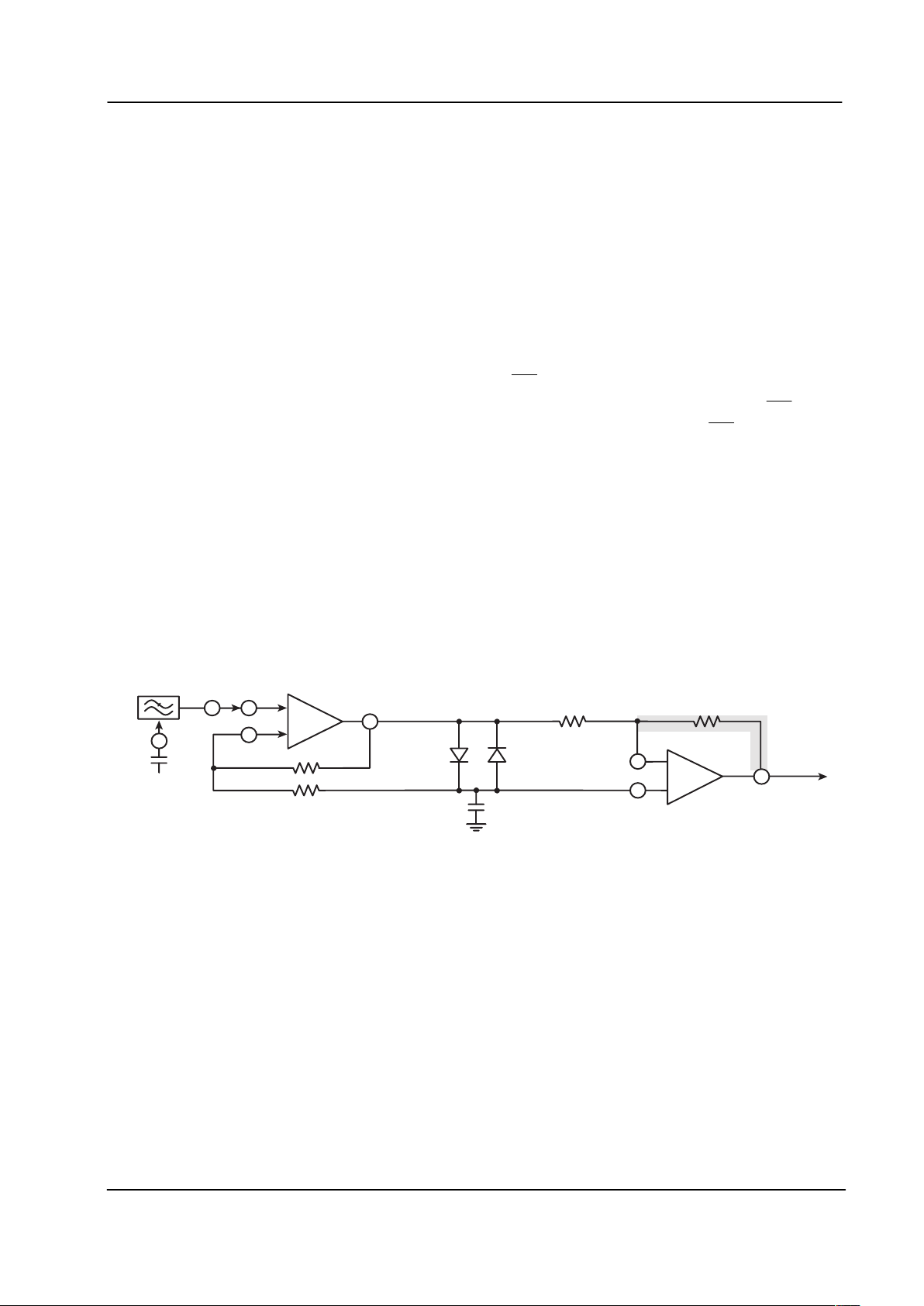
3.1.1 Using and External Op-Amp
For DC coupling the MX805A to the receiver’s discriminator output when using burst mode NRZ
communication, it is recommended that an additional, external Op-Amp is employed as configured in
Figure 4. This configuration will quickly compensate for sudden shift of DC input bas.
Components R9, R10, and R11, should be calculated to provide an accurate potential of 2.5VDC (equal to
V
BIAS
) at pin junction 15/16when using a discriminator input and 900mVP-P at the output of the external opamp. Note that the MX805A LPF has a 6dB gain. If additional filtering is required, C9 should be used, it
should be calculated with R9 to provide a lowpass cutoff frequency (f
CO
) of 500Hz.
Page 9

Sub-Audio Signaling Processor 9 MX805A
1998 MX-COM, Inc. www.mxcom.com Tel: 800 638 5577 336 744 5050 Fax: 336 744 5054 Doc. # 20480116.004
4800 Bethania Station Road, Winston-Salem, NC 27105-1201 USA All trademarks and service marks are held by their respective companies.
C9
D1
R3
100k
R9
R10
V
DD
R11
270k
D2
NOTE 6
(see p.4)
+
+
+
_
_
_
EXTERNAL
OP-AMP
MX805A
RX AMP
MX805A RX LPF
Gain = 6dB
D.C. RESTORATION
LEVEL SHIFT AND AMPLIFY
MX805A
COMP ARATOR
COMPARAT OR
OUT
COMPARAT OR IN
RX AMP IN
FROM RX
DISCRIMINATOR
19
20
14
13
21
17
16
15
15 F
m
Figure 4: MX805A Input Components using and External Op-Amp
4 General Description
4.1 Glossary
DCS Continuous Digitally Coded Squelch
CTCSS Continuous Tone Controlled Sub-Audio Squelch
DPL
TM
Digital Private Line
LTR
TM
Logic Trunked Radio
NRZ Non-Return-to-Zero
f
CO
Filter Cutoff frequency
f
CTCSS IN
Sub-Audio Rx frequency
f
CTCSS OUT
Sub-Audio Tx frequency
f
TONE
Tone frequency
f
XTAL
Xtal/Clock frequency
R
NRZRX
NRZ RX baud rate
R
NRZTX
NRZ TX baud rate
s
INPUT
Audio input signal.
4.2 Operating Modes
4.2.1 NRZ Encoding
The NRZ Encoder is formed by a shift register and the TX Sub-Audio Lowpass Filter. Data loaded from the
Command Data line is output one 8-bit byte at a time from the NRZ Tx Data Register. The output data level
may be adjusted and filtered. Data may be pre-emphasized via a C-BUS command. The expected Rx baud
rate is programmed as the NRZ Tx Baud Rate (R
NRZTX
). See Table 8
4.2.2 CTCSS Encoding
The CTCSS Tone Encoder is comprised of a clock divider programmed by an 11-bit binary number (Q)
loaded to the CTCSS Tx Frequency Register (See Table 8) via the C-BUS Command Data line.
The square-wave output of the encoder is fed through the Tx Level Adjust variable gain block to the Tx
Sub-Audio lowpass filter, a variable gain bandwidth circuit controlled by 4-bits (P) if the CTCSS Tx Frequency
Register. The Tx Sub-Audio output is a sine-wave. Standard and nonstandard sub-audio tones are available.
A CDCS turnoff tone may also be generated.
Page 10

Sub-Audio Signaling Processor 10 MX805A
1998 MX-COM, Inc. www.mxcom.com Tel: 800 638 5577 336 744 5050 Fax: 336 744 5054 Doc. # 20480116.004
4800 Bethania Station Road, Winston-Salem, NC 27105-1201 USA All trademarks and service marks are held by their respective companies.
4.2.3 NRZ Decoding
Input (NRZ type) sub-audio signals are filtered and the data clock extracted. Decoded data is serially loaded
into a shift register buffer. This data is output on 8-bit byte at a time as Reply Data from the NRZ Rx Data
Register to the microcontroller. The expected Rx baud rate is programmed as the NRZ Rx Baud Rate
(R
NRZRX
). See Table 8. Any codeword recognition can be carried out by software.
4.2.4 CTCSS Decoding
Received CTCSS signals are filtered, and coherence is increased by the digital noise filter. The quality of the
signal is assessed by measurement of the cycle–to-cycle period variance and, provided it is sufficiently good,
the frequency is measured over a period of 122.64ms (4.0MHz crystal).
If the average signal quality is consistently too low, NoTone is indicated; if not the input frequency is precisely
indicated in the CTCSS Rx Frequency Register in a binary form.
Any single sub-audio tone within the specified range may be selected, enabling a DCS turnoff tone of 134Hz)
to be decoded while in the NRZ Rx mode.
5 Controlling Protocol
Control of the MX805A Sub-Audio Signaling Processor’s operation is by communications between the
microcontroller and the MX805A internal registers on the C-BUS, using Address/Commands (A/Cs) and
appended instructions or data (See Figure 10). The use and content of these instructions is detailed in the
following paragraphs and tables. The Address Select Input enables the addressing of 2 separate MX805As
on the C-BUS to provide full-duplex signaling.
5.1 MX805A Internal Registers
5.1.1 Control Register (70H/78H)
Write only, control and configuration of the MX805A.
5.1.2 Status Register (71
H
/79H)
Read only, reporting of device functions.
5.1.3 CTCSS Rx Frequency Register (72
H
/7AH)
Read only, a 2-byte binary word indicating the frequency of the received sub-audio input.
5.1.4 CTCSS Tx Frequency/NRZ Tx or Rx Baud Rate Register (73
H
/7BH)
Write only, a 2-byte command to set the relevant parameters.
5.1.5 NRZ Rx Data Register (74
H
/7CH)
Read only, a single byte f received NRZ data.
5.1.6 NRZ Tx Data Register (75
H
/7DH)
Write only, to load a single byte of NRZ data for transmission.
5.1.7 Gain Set Register (76
H
/7EH)
Write only, a single byte to set the gain of the Tx Lowpass Filter.
Page 11

Sub-Audio Signaling Processor 11 MX805A
1998 MX-COM, Inc. www.mxcom.com Tel: 800 638 5577 336 744 5050 Fax: 336 744 5054 Doc. # 20480116.004
4800 Bethania Station Road, Winston-Salem, NC 27105-1201 USA All trademarks and service marks are held by their respective companies.
5.2 Address/Commands
The first byte of a loaded data sequence is always recognized by the C-BUS as an Address/Command (A/C)
byte. Instruction and data transactions to and from this device consist of an Address/Command byte followed
by either:
(i) further instructions or data
(ii) a Status or data Reply
Instructions and data are loaded and transferred, via C-BUS, in accordance with the timing information in
Figure 9 and Figure 11.
Placing the Address Select input at a logic “0” will address MX805A #1, a logic “1” will address MX805A #2.
Table 4 and Table 5 show the list of A/C bytes relevant to the MX805A
Command Assignment Address/Command (A/C) byte Data Bytes
Hex Binary
MSB LSB
General Reset 01 00000001
Write to Control Register 70 01110000 +1 byte instruction to Control
Register
Read Status Register 71 01110001 +1 byte reply from Status Register
Read CTCSS Rx Freq. Reg. 72 01110010 +2 byte reply of CTCSS Rx Data
Write to CTCSS Tx Freq./NRZ
Baud Rate Reg.
73 01110011 +2 byte instruction for Tx Frequency
and NRZ Tx/Rx baud rates
Read NRZ Rx Data Reg. 74 01110100 +1 byte binary data Reply
Write to NRZ Tx Data Reg. 75 01110101 +1 byte binary data Command
Write to Gain Set Reg. 76 01110110 +1 byte instruction for Tx Output
Table 4: MX805A #1 C-BUS Address/Commands – (Address Select input at a logic “0”)
Command Assignment Address/Command (A/C) byte Data Bytes
Hex Binary
MSB LSB
General Reset 01 00000001
Write to Control Register 78 01111000 +1 byte instruction to Control
Register
Read Status Register 79 01111001 +1 byte reply from Status Register
Read CTCSS Rx Freq. Reg. 7A 01111010 +2 byte reply of CTCSS Rx Data
Write to CTCSS Tx Freq./NRZ
Baud Rate Reg.
7B 01111011 +2 byte instruction for Tx Frequency
and NRZ Tx/Rx baud rates
Read NRZ Rx Data Reg. 7C 01111100 +1 byte binary data Reply
Write to NRZ Tx Data Reg. 7D 01111101 +1 byte binary data Command
Write to Gain Set Reg. 7E 01111110 +1 byte instruction for Tx Output
Table 5: MX805A #2 C-BUS Address/Commands – (Address Select input at a logic “1”)
Page 12

Sub-Audio Signaling Processor 12 MX805A
1998 MX-COM, Inc. www.mxcom.com Tel: 800 638 5577 336 744 5050 Fax: 336 744 5054 Doc. # 20480116.004
4800 Bethania Station Road, Winston-Salem, NC 27105-1201 USA All trademarks and service marks are held by their respective companies.
5.2.1 Write to Control Register - A/C 70H (78H) followed by 1 byte of Command Data
Table 6 shows the configurations available to the MX805A. Bits 5, 6, and 7 are used together to Enable and
Powersave circuits sections as required.
Setting Control Bits
MSB
Transmitted First
7 6 5 Enabled Powersaved
0
0
0
0
1
1
1
1
0
0
1
1
0
0
1
1
0
1
0
1
0
1
0
1
CTCSS Decoder
NRZ Decoder
CTCSS Encoder
NRZ Encoder
CTCSS Encoder and Decoder
NRZ Encoder and CTCSS Decoder
NRZ Decoder and CTCSS Decoder
NRZ Decoder
NRZ Decoder and Both Encoders
CTCSS Decoder and Both Encoders
All Decoders
All Decoders
NRZ Encoder and Decoder
No circuits
All Encoders
All Encodes except Tx Sub-Audio LPF
and CTCSS Decoder
4
1
0
Enable Audio Output – Used with Bit 3
Disable Audio Output – output to V
BIAS
3
1
0
Enable Sub-Audio Bandstop Filter (Audio Signal Path)
Bypass Sub-Audio Bandstop Filter
2
1
0
Enable All MX805A Interrupts
Disable All MX805A Interrupts
1
1
0
Set Rx Lowpass Filter Bandwidth to 180Hz – for low CTCSS tones or NRZ Data
Set Rx Lowpass Filter Bandwidth to 260Hz
0
1
0
All encoders and Decoders Powersaved
All Encoders and Decoders Enabled unless individually Powersaved
Table 6: Control Register
5.2.2 General Reset
Upon power-up the bits in the MX805A registers will be random (either 0 or 1). A General Reset Command
(01
H
) will be required to reset all devices on the C-BUS. It has the following effect on the MX805A:
Control Register Set to 00
H
Status Register Set to 00
H
NoTone Timer Discharged
Warning
: The following MX805A register configurations are not affected by a General Rest Command:
CTCSS Rx Frequency
CTCSS Tx Frequency/NRZ Baud Rate Register
NRZ Rx Data Register
NRZ Tx Data Register
Gain Set Register
Note
: Setting the Control Register in this way will set the MX805A to the CTCSS decode mode and overwrite
a “Powersave All” instruction. It should also be considered that a General Reset command will reset All
DBS800 ICs operating on the C-BUS.
Page 13

Sub-Audio Signaling Processor 13 MX805A
1998 MX-COM, Inc. www.mxcom.com Tel: 800 638 5577 336 744 5050 Fax: 336 744 5054 Doc. # 20480116.004
4800 Bethania Station Road, Winston-Salem, NC 27105-1201 USA All trademarks and service marks are held by their respective companies.
5.2.3 Read Status Register –A/C 71H (79H) followed by 1 byte of Rely Data.
The Status Register indicates the operational condition of the MX805A. Bits 0 to 5 are set individually to
indicate specific actions within the device. When a Status bit is set to a logic “1”, and Interrupt Request (IRQ)
output is generated. A read of the Status Register will reset the Interrupt and ascertain the state of this
register. Table 7 shows the conditions indicated by the Status bits.
Setting Set By Logic Cleared By Logic
MSB
Received First
7, 6
Not Used
0 Not Used 0
5
NRZ data transmission complete.
No new data is loaded.
1 1. Write to NRZ Data Reg., or
2. General Reset, or
3. NRZ Encoder Powersave
0
4
NRZ TX Data Buffer ready for next
data byte.
1 1. Write to NRZ TX Data Reg., or
2. General Rest, or
3. NRZ TX Powersave
0
3
New NRZ RX data received before
last byte was read.
1 1. Read NRZ RX Data Reg., or
2. General Reset, or
3. NRZ Decoder powersave
0
2
1 byte of NRZ data received 1 1. Read NRZ RX Data Reg., or
2. General Reset, or
3. NRZ Decoder powersave
0
1
NoTone timer period expired 1 1. Read Status Register, or
2. General Rest, or
3. CTCSS Decoder Powersave
0
0
RX Tone Measurement Complete 1 1. Read Status Register, or
2. General Reset, or
3. CTCSS Decoder Powersave
0
Table 7: Status Register
5.2.4 Read CTCSS RX Frequency Register –A/C 72
H
(7AH) followed by 2 bytes of Reply Data
5.2.4.1 Measurement of CTCSS RX Frequency (f
CTCSS IN
)
The input sub-audio signal (f
CTCSS IN
) is filtered, doubled and measured in the Frequency Counter over the
“measurement period” (122.64ms) (4.0MHz Xtal).
The measuring function counts the number of complete input cycles occurring within the measurement period
and the number of measuring-clock cycles necessary to make up one period.
When the measurement period of a successful decode is complete, the RX Tone Measurement bit in the
Status Register and the Interrupt bit are set.
The CTCSS RX Frequency Register will now indicated the sub-audio signal frequency (f
CTCSS IN
) in the form
of 2 data bytes (1 and 0) as illustrated in Figure 6.
Complete
Input
Cycle
Complete
Input
Cycle
Complete
Input
Cycle
Complete
Input
Cycle
Complete
Input
Cycle
Measuring
Clock
Cycles
Measurement Period
N
R
FIL TERED AND DOUBLED SUB-AUDIO INPUT SIGNAL 2 x f
CTCSS IN
Figure 5: Measurement of a CTCSS RX Frequency
Page 14

Sub-Audio Signaling Processor 14 MX805A
1998 MX-COM, Inc. www.mxcom.com Tel: 800 638 5577 336 744 5050 Fax: 336 744 5054 Doc. # 20480116.004
4800 Bethania Station Road, Winston-Salem, NC 27105-1201 USA All trademarks and service marks are held by their respective companies.
5.2.4.1.1 The Integer (N) –Byte 1
The binary number representing twice the number of cmplete input sub-audio cycle periods counted during
the measurement period of 122.64ms (4.0MHz crystal)
5.2.4.1.2 The Remainder (R) –Byte 0
A binary number representing the remainder part, R, of 2x the Sub-Audio Input Frequency. R = number of
specified measuring-clock cycles required to complete the specified measurement period (See N). The clock
cycle frequency is 4166.6Hz (4.0MHz crystal)
15
14
13
12 11
10
9
8
"0" "0"
Integer (N)
7
6
5
43
2
1
0
"0" "0"
Remainder (R)
Byte 1 Byte 0
CTCSS RX Frequency Register
(Reply Data)
(MSB) - Transmitted First
(Reply Data)
(LSB) - Transmitted Last
Figure 6: Format of the CTCSS RX Frequency Register
5.2.4.2 CTCSS RX Frequency Register
The format of the CTCSS RX Frequency Register is shown in Figure 6.
Bits 8 (LSB) to 13 (MSB) are used to represent the Integer (N). From Byte 1, valid values of
61N16N
i.e. values of N less than 16 and greater than 61 are not within the specified frequency band.
Bits 0 (LSB) to 5 (MSB) are used to represent the Remainder (R). From Byte 0, valid values of 31R
. This
register is not affected by the General Reset command (01H) and may adopt any random configuration at
Power-UP.
5.2.4.3 CTCSS RX Frequency Measurement Formulas
To assist in the production of “lookup” tables and limit-values in the microcontroller, and to provide guidance
upon the determination of N and R from a measured CTCSS frequency, the following formulas show the
derivation of the CTCSS RX Frequency (f
CTCSS IN
) from the measured data bytes (N and R).
5.2.4.3.1 f
CTCSS IN
In the measurement period of 122.64ms there are N cycles at 2 x f
CTCSS IN
and R clcok cycles at 4166.6Hz,
for any input frequency.
5.
f x 1920
f x N
-511INT R
f
xf511 x 1920
INT N
R)-(511 1920
f N
f
IN CTCSS
XTAL
XTAL
IN CTCSS
XTAL
IN CTCSS
Calculate N first
Example: (f
XTAL
= 4.00Mhz): f
CTCSS IN
= 100Hz N = 24 R = 11; f
CTCSS IN
= 250Hz N = 61 R = 3
5.2.4.4 NoTone Timing
The input sub-audio signal is monitored by the Frequency Assessment Circuitry. Before any NoTone action is
enabled, the MX805A must have achieved at least one successful “Tone Measurement Complete” action.
If there is no signal or the signal is of a consistently poor quality, the NoTone timer will start to charge via the
timing components. When the timing period has expired (at V
DD
/2), an Interrupt and a Status bit (NoTone
Timer Expired) are generated. This is a one-shot function which is rest by a “Tone Measurement Complete”
interrupt.
Page 15

Sub-Audio Signaling Processor 15 MX805A
1998 MX-COM, Inc. www.mxcom.com Tel: 800 638 5577 336 744 5050 Fax: 336 744 5054 Doc. # 20480116.004
4800 Bethania Station Road, Winston-Salem, NC 27105-1201 USA All trademarks and service marks are held by their respective companies.
5.2.5 Write to CTCSS TX Frequency/NRZ Baud Data Rate Register –A/C 73H (7BH) followed by 2
bytes of Command Data.
The information loaded to this register will set either the:
(a) CTCSS TX Tone Frequency f
CTCSS OUT
(b) NRZ TX Baud Rate R
NRZ TX
(c) NRZ RX Baud Rate R
NRZ RX
The chosen mode for this register (a, b, or c) is determined by the MX805A modes enabled by the Control
Register, as shown in Table 8.
Control Register Bits
765
MX805A Mode
Enabled
CTCSS TX/NRZ Baud Rate
Register Function
0
0
0
0
1
1
1
1
0
0
1
1
0
0
1
1
0
1
0
1
0
1
0
1
CTCSS Decode
NRZ Decode
CTCSS Decode
NRZ Encode
CTCSS Encode and Decode
NRZ Encode & CTCSS Decode
NRZ & CTCSS Decode
NRZ Decode
NRZ RX Baud Rate
CTCSS TX Frequency
NRZ TX Baud Rate
CTCSS TX Frequency
NRZ TX Baud Rate
NRZ RX Baud Rate
NRZ RX Baud Rate
Table 8 CTCSS Frequency/NRZ Baud Rate Register Configurations
5.2.5.1 Data Format
Data is transmitted to this register as 2 bytes of Command Data in the form illustrated in the diagram below.
This register is not affected by the General Rest Command (01H) and may adopt any random configuration at
power-up.
15
14
13
12 11
10
9
8
"0"
P
7
6
5
43
2
1
0
Q
Byte 1 Byte 0
CTCSS TX Frequency/NRZ Baud Rate Register
(Command Data)
(MSB) - Loaded First
(Command Data)
(LSB) - Loaded Last
Figure 7: Format of the CTCSS TX Frequency/NRZ Baud Rate Register
5.2.5.2 Command Words P and Q
The two words, P and Q, loaded to this register are interpreted as:
P = a binary number to set the TX Sub-Audio Lowpass filter bandwidth (applicable to NRX and CTCSS
modes).
Q = A binary number to set the frequency r baud rate of the selected functon.
Page 16

Sub-Audio Signaling Processor 16 MX805A
1998 MX-COM, Inc. www.mxcom.com Tel: 800 638 5577 336 744 5050 Fax: 336 744 5054 Doc. # 20480116.004
4800 Bethania Station Road, Winston-Salem, NC 27105-1201 USA All trademarks and service marks are held by their respective companies.
5.2.5.2.1 Command Word P
Bits
LSB
15 14 13 12 P LPF Bandwidth
0
0
0
0
0
0
1
0
0
1
1
1
1
0
1
1
0
0
1
1
0
0
1
0
1
0
1
0
2
3
4
5
6
7
8
300Hz
200Hz
150Hz
120Hz
100Hz
85.7Hz
75Hz
Table 9: Valid Values of P
Bits 12 to 15 are used to produce the data word “P” as shown in Table 9. The cutoff frequency f
C/O
(0.5dB
point) of the TX Sub-Audio Lowpass filter is calculated as:
C/O
XTAL
XTAL
C/O
f33.20832
f
P
P x 208.33 x 32
f
f
Table 9 is provided as and example and calculated using a Xtal/Clock (f
XTAL
) frequency of 4.00MHz. As
illustrated, only values of “P” of 2 to 8 are usable
5.2.5.2.2 Command Word Q
Bits 0 to 10 (See Figure 7) are used to produce the data word “Q” which sets one of the parameters described
below. As you can see, Command Word “Q” could be used to produce a parameter outside that specified in
the “Characteristics” section of this data bulletin. Care should be taken not to do this. Examples for limits of
“Q” in each operational configuration are included. “Q” = 0 is not valid in the following calculations. Bit 11 is
not used and must be set to logic “0”.
(a) CTCSS TX Tone Frequency (f
CTCSS OUT
)
Hz
f x 32
f
Q"" so
Hz
Q"" x 32
f
f
OUT CTCSS
XTAL
XTAL
OUT CTCSS
f
CTCSS OUT
So “Q”
f
CTCSS OUT
So “Q”
=
=
=
=
67Hz
1866
250Hz
500
“11101001010”
“00111110100”
(b) NRZ TX Baud Rate (R
NRZ TX
)
TZ NRZ
XTAL
XTAL
TZ NRZ
R x 32
f
Q"" so
bits/sec
Q"" x 32
f
R
R
NRZ TX
So “Q”
R
NRZ TX
So “Q”
=
=
=
=
67bits/sec
1866
300bits/sec
417
“11101001010”
“00110100001”
(c) NRZ RX Baud Rate (R
NRZ RX
)
RX NRZ
XTAL
XTAL
RX NRZ
R x 352
f
Q"" so
bits/sec
Q"" x 11 x 32
f
R
R
NRZ RX
So “Q”
R
NRZ RX
So “Q”
=
=
=
=
67bits/sec
114
300bits/sec
38
“00001110010”
“00000100110”
Page 17

Sub-Audio Signaling Processor 17 MX805A
1998 MX-COM, Inc. www.mxcom.com Tel: 800 638 5577 336 744 5050 Fax: 336 744 5054 Doc. # 20480116.004
4800 Bethania Station Road, Winston-Salem, NC 27105-1201 USA All trademarks and service marks are held by their respective companies.
5.2.6 Read NRZ RX Data Register – A/C 74H (7CH) followed by 1 byte Reply Data
Received NRZ data bits are organized into bytes and made available to the microcontroller via the Reply Data
line. As 8 bits are received into this register and interrupt is generated to indicate that a complete byte has
been received. This byte must be read before the arrival of the last (8
th
) bit of the next incoming byte. If this
in not done, an interrupt to indicate this condition will be generated and the previous RX data is discarded.
See Table 7.
Word synchronization is not provided. Byte synchronization and any codeword recognition will be performed
by the host microcontroller. The RX baud rate is set by writing to the CTCSS TX Frequency/NRZ Baud Rate
Register (73
H
/7BH). The first bit received is the first bit sent to the microcontroller.
This register is not affected by the General Reset Command (01H), and may adopt random configuration at
Power-Up.
5.2.7 Write to NRZ TX Data Register – A/C 75
H
(7DH) followed by 1 byte of Command Data.
A byte for transmission is loaded from the C-BUS Command Data line with the A/C. The first data bit
received via the C-BUS is transmitted first. The transmitter operation is non-inverting.
The first data byte loaded after the NRZ Encoder is enabled (Control Register) initiates the transmission
sequence and an interrupt will be generated when the NRZ TX Data Buffer is ready for the next data byte.
Subsequently, interrupts occur for every 8 bits transmitted.
Transmission is terminated, the TX Sub-Audio Output is placed at V
BIAS
, and a interrupt is generated if the
next byte is not loaded within 7 bit periods. See Table 7.
This register is not affected by the General Reset Command (01
H
), and may adopt any random configuration
at Power-Up.
5.2.8 Write to Gain Set Register – A/C 76
H
(7EH) followed by 1 byte of Command Data
5.2.8.1 Gain Set Register Settings:
The settings of this register control the CTCSS and NRZ signal level that is presented at the TX Sub-Audio
Output.
Bit 3, when enabled, is used to produce a pre-emphasis effect on the NRZ TX Data by increasing the gain of
the data bit before a level change (See Figure 8), by 1.72dB to make that data pulse level slightly more
positive (or negative). The signal level will be 1.72dB greater that that set by Bits 0 to 2. If the TX Sub-Audio
Output level is set to +2.58dB, the pre-emphasis level will be +4.3dB.
The pre-emphasis function will remain enabled until disabled by setting Bit 3 to a logic “0”. If this function
remains enabled when using the CTCSS Encoder, the output signal may be adversely affected. Therefore
this function should be enabled when in the NRZ Encode mode.
This register is not affected by the General Reset Command (01
H
), and may adopt any random configuration
at Power-Up.
Setting Gain Setting
7 6 5 4 Transmitted Bit 7 First
0000
3 Pre-Emphasis Setting
1
0
1.72dB Gain Enabled
1.72dB Gain Disabled
2 1 0 Tx Level Adjust Gain Setting
0
0
0
0
1
1
1
1
0
0
1
1
0
0
1
1
0
1
0
1
0
1
0
1
-2.58dB
–1.72dB
–0.86dB
0dB
+0.86dB
+1.72dB
+2.58dB
Not Used
Table 10: Gain Set Register Settings
Page 18

Sub-Audio Signaling Processor 18 MX805A
1998 MX-COM, Inc. www.mxcom.com Tel: 800 638 5577 336 744 5050 Fax: 336 744 5054 Doc. # 20480116.004
4800 Bethania Station Road, Winston-Salem, NC 27105-1201 USA All trademarks and service marks are held by their respective companies.
15
14
13
12 11
10
9
8
"0"
P
7
6
5
43
2
1
0
Q
Byte 1 Byte 0
CTCSS TX Frequency/NRZ Baud Rate Register
(Command Data)
(MSB) - Loaded First
(Command Data)
(LSB) - Loaded Last
Figure 8: Gain Set with Pre-Emphasisi
6 Performance Specifications
6.1 Electrical Specifications
6.1.1 Absolute Maximum Limits
Exceeding these maximum ratings can result in damage to the device.
General Notes Min. Typ. Max. Units
Supply (VDD-VSS) -0.3 7.0 V
Voltage on any pin to V
SS
-0.3 VDD + 0.3 V
Current
V
DD
-30 30 mA
V
SS
-30 30 mA
Any other pin -20 20 mA
P / DW / LH Packages
Total allowable Power dissipation
at T
AMB
= 25C
800 mW
Derating above 25C
10
mW/C above 25C
Operating Temperature -40 85
C
Storage Temperature -55 125
C
Table 11: Absolute Maximum Ratings
6.1.2 Operating Limits
Correct Operation of the device outside these limits is not implied.
Notes Min. Typ. Max. Units
Supply (VDD-VSS) 4.5 5.0 5.5 V
Operating Temperature -40 85
C
Xtal Frequency 4.0 MHz
Table 12: Operating Limits
Page 19

Sub-Audio Signaling Processor 19 MX805A
1998 MX-COM, Inc. www.mxcom.com Tel: 800 638 5577 336 744 5050 Fax: 336 744 5054 Doc. # 20480116.004
4800 Bethania Station Road, Winston-Salem, NC 27105-1201 USA All trademarks and service marks are held by their respective companies.
6.1.3 Operating Characteristics
For the following conditions unless otherwise specified.
V
DD
= 5.0V @ T
AMB
= 25C
Xtal/Clock Frequency = 4.0MHz, Audio Level 0dB ref. = 308mV
RMS
@ 1kHz
Composite Signal = 308mV
RMS
@ 1kHz + 75mV
RMS
Noise + 31mV
RMS
Sub-Audio signal
Noise Bandwidth = 5kHz Band Limited Gaussian
Notes Min. Typ. Max. Units
Static Values
Supply Current
All Functions Enabled 5.0 7.0 mA
All Functions Disabled 2.0 3.0 mA
Powersave All 0.9 1.5 mA
Analog Impedances
RX Sub-Audio Input 350.0 1500.0
k
Audio Input 350.0
k
Audio Bypass Switch On 5 2.0
k
Audio Bypass Switch OFF 5 1.0 6.5
M
RX Amp Input (+ and -) 1.0 6.5
M
Comparator Input (+ and -) 1.0 6.5
M
RX Sub-Audio Output 2.0
k
TX Sub-Audio Output
Encoder Enabled 5 2.0
k
Encoder Disabled 5 500.0
k
Audio Output
Encoder Enabled 5 2.0
k
Encoder Disabled 5 500.0
k
RX Amp and Comparator Outputs
Large Signal 6.0
k
Small Signal 600.0
k
Dynamic Values
Digital Interface
Input Logic 1 1 3.5 V
Input Logic 0 1 1.5 V
Output Logic 1 (IOH = -120mA) 2 4.6 V
Output Logic 1 (IOL = -360mA) 3 0.4 V
I
OUT
Tristate (Logic 1 or 0) 3 4.0
A
Input Capacitance 1 7.5 pF
Logic Input Current (VIN = 0 to 5.0V) 1 1.0
A
IOX (V
OUT
= 5.0V) 4 4.0
A
Page 20

Sub-Audio Signaling Processor 20 MX805A
1998 MX-COM, Inc. www.mxcom.com Tel: 800 638 5577 336 744 5050 Fax: 336 744 5054 Doc. # 20480116.004
4800 Bethania Station Road, Winston-Salem, NC 27105-1201 USA All trademarks and service marks are held by their respective companies.
Notes Min. Typ. Max. Units
Overall Performance
dB
CTCSS - Decode kHz
Sensitivity (Composite Signal) 6 -20.0 -26.0 dB
Response Time (Composite Signal)
100Hz to 257Hz Tone 210.0 250.0 ms
65Hz Tone 9 210.0 384.0 ms
Tone Measurement Resolution 0.2 %
Tone Measurement Accuracy -0.5 0.5 %
NoTone Response Time (Composite Signal) 7 175.0 250.0 ms
False tone Interrupts (Noise Input Only) 10 20.0 /Hr
CTCSS Encode
Frequency Range 65.0 257.0 Hz
Tone Frequency Resolution 0.2 %
Tone Amplitude Tolerance 12 -1.0 1.0 dB
Rise Time (to 90%) 30.0 ms
Fall Time (to 10%) 50.0 ms
Total Harmonic Distortion 5.0 %
NRX – Decode
RX Bit Rate Sync Time 2 edge
RX Bit Error Rate 11 1 x 10
-3
P
(ERROR)
NRZ – TX
TX Bit Rate 67.0 300.0 bits/sec
TX LPF (3dB) Bandwidth 75.0 300.0 Hz
Sub-Audio TX Output Level
CTCSS 0 dB
NRZ 0.871 V
P-P
Amplitude Adjustment Range -2.58 2.58 dB
Adjustment Step Size (7 Steps) 8 0.86 dB
Sub-Audio Bandstop Filter
Passband 297.0 3000.0 Hz
Passband Gain (@ 1.0kHz) 0 dB
Passband Ripple (with respect to gain @ 1.0Hz) -1.5 0.5 dB
Stopband Gain < 250Hz 36.0 dB
Residual Hum and Noise -50.0 -45.7 dB
Alias Frequency 62.5 kHz
Receive Lowpass Filter (See Figure 9)
Cutoff Frequency (-3dB) 280.0 Hz
Passband Gain 6.0 dB
Xtal/Clock Frequency (f
XTAL
) 4.0 6.1 MHz
Table 13: Operating Characteristics
Page 21

Sub-Audio Signaling Processor 21 MX805A
1998 MX-COM, Inc. www.mxcom.com Tel: 800 638 5577 336 744 5050 Fax: 336 744 5054 Doc. # 20480116.004
4800 Bethania Station Road, Winston-Salem, NC 27105-1201 USA All trademarks and service marks are held by their respective companies.
Operating Characteristics Notes:
1. Device control pins: Serial Clock, Command Data,
Wake , and CS .
2. Reply Data Output
3. Reply Data and
IRQ
outputs
4. Leakage current into the “OFF”
IRQ output.
5. See Control Register
6. With input gain components set as recommended in Figure 2.
7. Probability 97%
8. See Gain Set Register.
9. For f
CTCSS
IN of 65Hz to 100Hz, Response Time tR = (100/f
Tone
) x 250ms.
10. Distributed across the RX Frequency band
11. With 10dB signal-to-noise ratio in a bit-rate bandwidth.
12. At any gain setting of Gain Register.
10dB/division
0
0
800
Xtal = 4.0 MHz
V = 5.0V
DD
Frequency (Hz)
Signal
Level
(dB)
100
300 400
500
600
700200
Figure 9: Typical Frequency Response of RX Lowpass Filter
Page 22

Sub-Audio Signaling Processor 22 MX805A
1998 MX-COM, Inc. www.mxcom.com Tel: 800 638 5577 336 744 5050 Fax: 336 744 5054 Doc. # 20480116.004
4800 Bethania Station Road, Winston-Salem, NC 27105-1201 USA All trademarks and service marks are held by their respective companies.
6.1.4 Timing
Timing Parameters for two-way communications between the C and the MX805A on the C-BUS are shown
in Table 14.
C-BUS Timing Min. Typ. Max. Units
t
CSE
Chip Select Low to First Serial Clock Rising Edge 2.0
s
t
CHS
Last Serial Clock Rising Edge to Chip Select High 4.0
s
t
CSOFF
Chip Select High 2.0
s
t
NXT
Command Data Inter-Byte Time 4.0
s
t
CK
Serial Clock Period 2.0
s
t
CH
Decoder or Encoder Clock High 500 ns
t
CL
Decoder or Encoder Clock Low 500 ns
t
CDS
Command Data Set-Up Time 250 ns
t
CDH
Command Data Hold Time 0 ns
t
RDS
Reply Data Set-Up Time 250 ns
t
RDH
Reply Data Hold Time 50.0 ns
t
HIZ
Chip Select High to Reply Data High – Z 2.0
s
Table 14: Timing Information
Notes:
1. Command Data is transmitted to the peripheral MSB (bit 7) first, LSB (bit 0) last. Reply Data is read from
the MX805A MXB (bit 7) first, LSB (bit 0) last.
2. Data is clocked into the MX805A and into the microcontroller on the rising Serial Clock edge.
3. Loaded data instructions are acted upon at the end of each individual, loaded byte.
4. To allow for differing microcontroller serial interface formats, the MX805A will work with either polarity
Serial clock pulses.
CHIP SELECT
SERIAL CLOCK
COMMAND DATA
REPLY DATA
ADDRESS/COMMAND
BYTE
FIRST DATA BYTE LAST DATA BYTE
FIRST REPLY DAT A BYTE LAST REPLY DATA BYTE
Logic level is not important
MSB LSB
76543210 76543210
76543210
MSB
LSB
76543210
76543210
t
t
t
CSOFF
t
CSH
HIZ
t
NXT
t
NXT
CK
t
CSE
Figure 10: C-BUS Timing Information
Page 23

Sub-Audio Signaling Processor 23 MX805A
1998 MX-COM, Inc. www.mxcom.com Tel: 800 638 5577 336 744 5050 Fax: 336 744 5054 Doc. # 20480116.004
4800 Bethania Station Road, Winston-Salem, NC 27105-1201 USA All trademarks and service marks are held by their respective companies.
t
t
t
t
t
t
t
CH
CK
CDH
RDH
RDS
CDS
CL
70% VDD
30% VDD
COMMAND DATA
(from µC)
SERIAL CLOCK
(from C)
REPLY DA TA
(to µC)
Figure 11: Timing Relationships for C-BUS Information Transfer
6.2 Packages
NOTE: All dimensions in inches(mm.)
Angles are in degrees
PackageTolerances
A
B
C
E
E1
H
TYP. MAX.MIN.DIM.
J
J1
P
Y
T
K
L
0.220 (5.59)
0.555 (14.04)
0.670 (17.02)
7°
0.160 (4.05)
1.270 (32.26)
0.151 (3.84)
0.100 (2.54)
0.121 (3.07)
0.600 (15.24)
0.590 (14.99) 0.625 (15.88)
0.015 (0.38) 0.045 (1.14)
0.008 (0.20) 0.015 (0.38)
0.015 (0.38) 0.023 (0.58)
0.040 (1.02) 0.065 (1.65)
0.066 (1.67) 0.074 (1.88)
1.200 (30.48)
0.500 (12.70)
H
K
L
J1J1
JJ
PP
CC
B
B
A
A
PIN1PIN1
TT
E
E
E1
E1
Y
Figure 12: 24-pin PDIP Mechanical Outline:
Order as part no. MX805AP
0.597 (15.16)
PackageTolerances
A
B
C
E
H
TYP. MAX.MIN.DIM.
J
P
X
W
T
Y
K
L
0.105 (2.67)
0.093 (2.36)
0.419 (10.64)
45°
7°
0°
10°
0.050 (1.27)
0.046 (1.17)
0.613 (15.57)
0.299 (7.59)
0.050 (1.27)
0.016 (0.41)
0.390 (9.90)
0.020 (0.51)0.003 (0.08)
0.009 (0.23)
0.0125 (0.32)
0.013 (0.33)
0.020 (0.51)
0.036 (0.91)
0.286 (7.26)
Z
NOTE: All dimensions in inches(mm.)
Angles are in degrees
5°
5°
PIN 1
A
B
X
P
J
Y
C
H
K
E
L
T
W
Z
Alternative Pin
Location
Marking
Figure 13: 24-pin SOIC Mechanical Outline:
Order as part no. MX805ADW
Page 24

Sub-Audio Signaling Processor 24 MX805A
1998 MX-COM, Inc. www.mxcom.com Tel: 800 638 5577 336 744 5050 Fax: 336 744 5054 Doc. # 20480116.004
4800 Bethania Station Road, Winston-Salem, NC 27105-1201 USA All trademarks and service marks are held by their respective companies.
PackageTolerances
NOTE: All dimensions in inches (mm.)
Angles are in degrees
A
B
C
D
E
H
P
F
G
TYP. MAX.MIN.DIM.
K
J
W
T
Y
0.435 (11.05)
0.435 (11.05)
0.051 (1.30)
0.009 (0.22)
6°
30°
0.409 (10.40)
0.409 (10.40)
0.146 (3.70)
0.417 (10.60)
0.417 (10.60)
0.049 (1.24)
0.006 (0.152)
0.250 (6.35)
0.250 (6.35)
0.023 (0.58)
0.047 (1.19)
0.022 (0.55)0.018 (0.45)
0.380 (9.61)
0.380 (9.61)
0.128 (3.25)
0.048 (1.22)
45°
F
G
P
A
D
B
E
PIN 1
W
C
J
K
Y
W
H
T
Figure 14: 24-pin PLCC Mechanical Outline:
Order as part no. MX805ALH
 Loading...