

Page 1
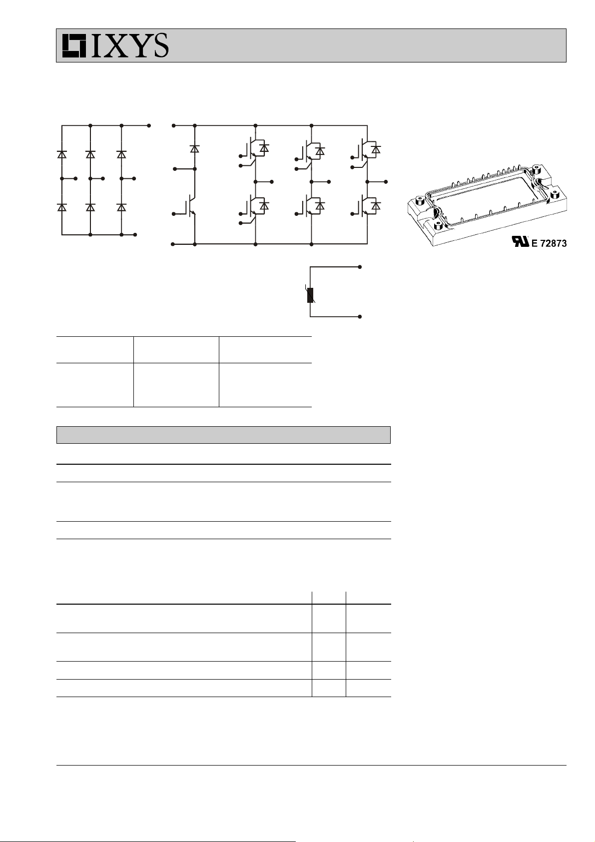
Converter - Brake - Inverter Module (CBI2)
22
21
MUBW 15-12 A7
T1
T2
D1
6
D2
D11 D13 D15
23
1
D12
D14
D16
23
14
7
D7
16
15
T7
11
10
24
Three Phase Brake Chopper Three Phase
Rectifier Inverter
V
I
DAVM
I
FSM
RRM
= 1600V V
= 36 A I
= 300 A V
= 1200 V V
CES
= 20 A I
C25
= 2.3 V V
CE(sat)
CES
C25
CE(sat)
= 1200 V
= 35 A
= 2.1 V
T3
D3
D4
20
19
5
18
17
T4
12 13
NTC
T5
T6
D5
4
D6
8
9
Input Rectifier Bridge D11 - D16
Symbol Conditions Maximum Ratings
V
I
FAV
I
DAVM
I
FSM
P
RRM
tot
TC = 80°C; sine 180° 25 A
TC = 80°C; rectangular; d = 1/3 24 A
TVJ = 25°C; t = 10 ms; sine 50 Hz 300 A
TC = 25°C 100 W
1600 V
Symbol Conditions Characteristic Values
(T
= 25°C, unless otherwise specified)
V
I
t
R
VJ
F
R
rr
thJC
IF = 15 A; TVJ = 25°C 1.3 1.6 V
TVJ = 125°C 1.3 V
VR = V
TVJ = 25°C 0.15 mA
RRM;
TVJ = 125°C 1.2 mA
VR = 100 V; IF = 15 A; di/dt = -15 A/µs 1 µs
(per diode) 1.3 K/W
min. typ. max.
Application: AC motor drives with
●
Input from single or three phase grid
●
Three phase synchronous or
asynchronous motor
●
electric braking operation
Features
●
High level of integration - only one power
semiconductor module required for the
whole drive
●
Fast rectifier diodes for enhanced EMC
behaviour
●
NPT IGBT technology with low
saturation voltage, low switching
losses, high RBSOA and short circuit
ruggedness
●
Epitaxial free wheeling diodes with
Hiperfast and soft reverse recovery
●
Industry standard package with insulated
copper base plate and soldering pins for
PCB mounting
●
Temperature sense included
IXYS reserves the right to change limits, test conditions and dimensions.
© 2001 IXYS All rights reserved
105
1 - 8
Page 2
MUBW 15-12 A7
Output Inverter T1 - T6
Symbol Conditions Maximum Ratings
V
CES
V
GES
V
GEM
I
C25
I
C80
RBSOA VGE = ±15 V; RG = 82 Ω; TVJ = 125°CI
t
SC
(SCSOA) non-repetitive
P
tot
TVJ = 25°C to 150°C 1200 V
Continuous
Transient
±
20 V
±
30 V
TC = 25°C35A
TC = 80°C25A
= 35 A
Clamped inductive load; L = 100 µH V
V
= V
CE
; VGE = ±15 V; RG = 82 Ω; TVJ = 125°C10µs
CES
CM
CEK
≤ V
CES
TC = 25°C 180 W
Symbol Conditions Characteristic Values
(T
= 25°C, unless otherwise specified)
V
V
I
CES
CE(sat)
GE(th)
VJ
IC = 15 A; VGE = 15 V; TVJ = 25°C 2.1 2.6 V
TVJ = 125°C 2.3 V
IC = 0.6 mA; VGE = V
V
= V
CE
CES; VGE
CE
= 0 V; TVJ = 25°C 0.9 mA
TVJ = 125°C 0.9 mA
min. typ. max.
4.5 6.5 V
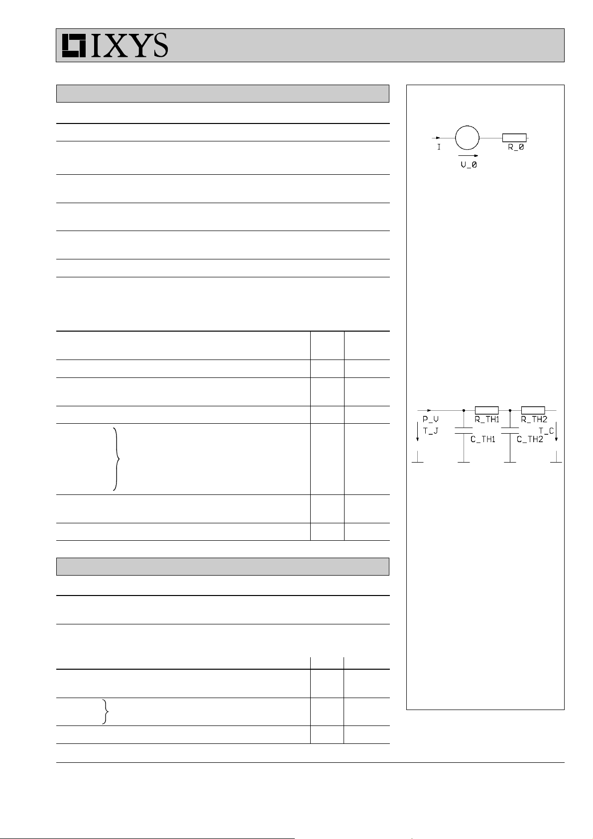
Equivalent Circuits for Simulation
Conduction
D11 - D16
Rectifier Diode (typ. at TJ = 125°C)
T1 - T6 / D1 - D6
IGBT (typ. at VGE = 15 V; TJ = 125°C)
Free Wheeling Diode (typ. at TJ = 125°C)
T7 / D7
IGBT (typ. at VGE = 15 V; TJ = 125°C)
Free Wheeling Diode (typ. at TJ = 125°C)
Thermal Response
V0 = 1.08 V; R0 = 15 m
V0 = 1.37 V; R0 = 62 m
V0 = 1.32 V; R0 = 30 m
V0 = 1.32 V; R0 = 131 m
V0 = 1.39 V; R0 = 56 m
Ω
Ω
Ω
Ω
Ω
I
GES
t
d(on)
t
r
t
d(off)
t
f
E
E
C
Q
R
on
off
ies
Gon
thJC
VCE = 0 V; VGE = ± 20 V 200 nA
100 ns
Inductive load, T
= 125°C
VJ
VCE = 600 V; IC = 15 A
VGE = ±15 V; RG = 82 Ω
70 ns
500 ns
70 ns
2.3 mJ
1.8 mJ
VCE = 25 V; VGE = 0 V; f = 1 MHz 1000 pF
V
= 600V; VGE = 15 V; IC = 15 A 70 nC
CE
(per IGBT) 0.7 K/W
Output Inverter D1 - D6
Symbol Conditions Maximum Ratings
I
F25
I
F80
TC = 25°C28A
TC = 80°C18A
Symbol Conditions Characteristic Values
min. typ. max.
V
F
I
RM
t
rr
R
thJC
IF = 15 A; VGE = 0 V; TVJ = 25°C 2.7 V
TVJ = 125°C 1.8 V
IF = 15 A; diF/dt = -400 A/µs; TVJ = 125°C16A
VR = 600 V; VGE = 0 V 130 ns
(per diode) 2.1 K/W
D11 - D16
Rectifier Diode (typ.)
C
= 0.106 J/K; R
th1
C
= 0.79 J/K; R
th2
th1
= 0.239 K/W
th2
T1 - T6 / D1 - D6
IGBT (typ.)
C
= 0.156 J/K; R
th1
C
= 1.162 J/K; R
th2
th1
th2
Free Wheeling Diode (typ.)
C
= 0.065 J/K; R
th1
C
= 0.639 J/K; R
th2
th1
th2
T7 / D7
IGBT (typ.)
C
= 0.09 J/K; R
th1
C
= 0.809 J/K; R
th2
= 0.954 K/W
th1
th2
Free Wheeling Diode (typ.)
C
= 0.043 J/K; R
th1
C
= 0.54 J/K; R
th2
th1
= 0.462 K/W
th2
= 1.06 K/W
= 0.545 K/W
= 0.155 K/W
= 1.758 K/W
= 0.342 K/W
= 0.246 K/W
= 2.738 K/W
© 2001 IXYS All rights reserved
2 - 8
Page 3
Brake Chopper T7
Symbol Conditions Maximum Ratings
MUBW 15-12 A7
V
CES
V
GES
V
GEM
I
C25
I
C80
RBSOA VGE = ±15 V; RG = 82 Ω; TVJ = 125°CI
t
SC
(SCSOA) non-repetitive
P
tot
TVJ = 25°C to 150°C 1200 V
Continuous
Transient
±
20 V
±
30 V
TC = 25°C20A
TC = 80°C15A
= 20 A
Clamped inductive load; L = 100 µH V
V
= 720 V; VGE = ±15 V; RG = 82 Ω; TVJ = 125°C10µs
CE
CM
CEK
≤ V
CES
TC = 25°C 105 W
Symbol Conditions Characteristic Values
= 25°C, unless otherwise specified)
(T
V
V
I
CES
I
GES
t
d(on)
t
r
t
d(off)
t
f
E
E
C
Q
R
CE(sat)
GE(th)
on
off
ies
Gon
thJC
VJ
IC = 10 A; VGE = 15 V; TVJ = 25°C 2.3 2.7 V
TVJ = 125°C 2.7 V
IC = 0.4 mA; VGE = V
V
= V
CE
CES; VGE
CE
= 0 V; TVJ = 25°C 0.5 mA
TVJ = 125°C 0.3 mA
VCE = 0 V; VGE = ± 20 V 200 nA
Inductive load, TVJ = 125°C
VCE = 600 V; IC = 10 A
VGE = ±15 V; RG = 82 Ω
VCE = 25 V; VGE = 0 V; f = 1 MH z 600 pF
V
= 600 V; VGE = 15 V; IC = 10 A 45 nC
CE
min. typ. max.
4.5 6.5 V
50 ns
40 ns
290 ns
60 ns
1.2 mJ
1.1 mJ
1.2 K/W
Brake Chopper D7
Symbol Conditions Maximum Ratings
V
RRM
I
F25
I
F80
TVJ = 25°C to 150°C 1200 V
TC = 25°C17A
TC = 80°C11A
Symbol Conditions Characteristic Values
min. typ. max.
V
F
I
R
I
RM
t
rr
R
thJC
IF = 10 A; TVJ = 25°C 2.9 V
TVJ = 125°C 1.9 V
VR = V
TVJ = 25°C 0.06 mA
RRM;
TVJ = 125°C 0.07 mA
IF = 10 A; diF/dt = -400 A/µs; TVJ = 125°C13A
VR = 600 V 110 ns
3.2 K/W
© 2001 IXYS All rights reserved
3 - 8
Page 4
Temperature Sensor NTC
Symbol Conditions Characteristic Values
min. typ. max.
MUBW 15-12 A7
R
25
B
25/50
T = 25°C 4.75 5.0 5.25 kΩ
3375 K
Module
Symbol Conditions Maximum Ratings
T
VJ
T
JM
T
stg
V
ISOL
M
d
Operating -40...+125 °C
150 °C
-40...+125 °C
I
≤ 1 mA; 50/60 Hz 2500 V~
ISOL
Mounting torque (M5) 2.7 - 3.3 Nm
Symbol Conditions Characteristic Values
min. typ. max.
R
pin-chip
d
S
d
A
R
thCH
Creepage distance on surface 6 mm
Strike distance in air 6 mm
with heatsink compound 0.02 K/W
5mΩ
Weight 180 g
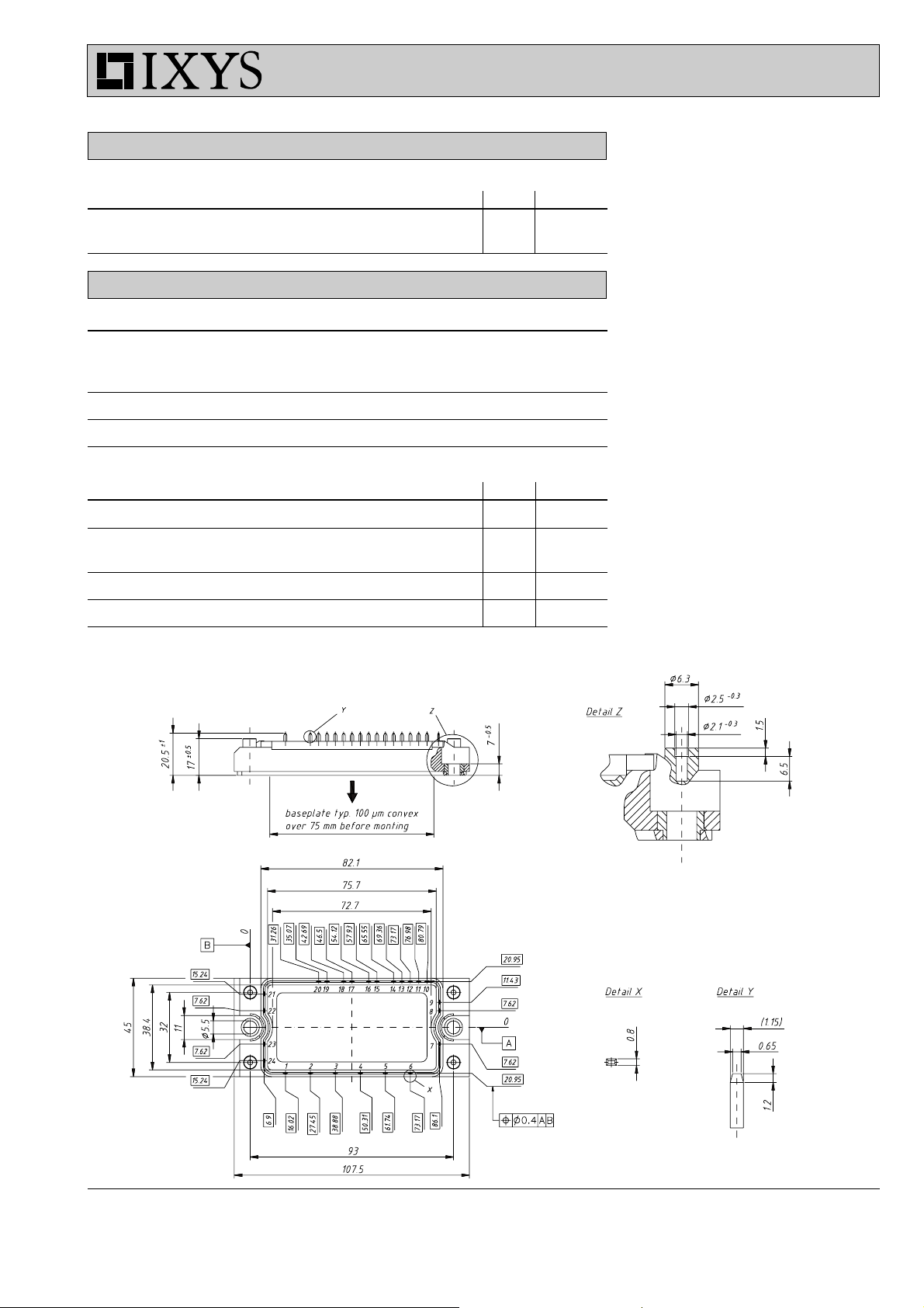
Dimensions in mm (1 mm = 0.0394")
© 2001 IXYS All rights reserved
4 - 8
Page 5
Input Rectifier Bridge D11 - D16
50
A
40
I
F
30
20
TVJ= 125°C
T
= 25°C
VJ
I
100
FSM
50Hz, 80% V
A
80
60
40
RRM
TVJ= 45°C
TVJ= 150°C
MUBW 15-12 A7
3
10
2
A
s
I2t
TVJ= 45°C
TVJ= 150°C
10
2
10
0
0.0 0.4 0.8 1.2 1.6 2.0
V
V
F
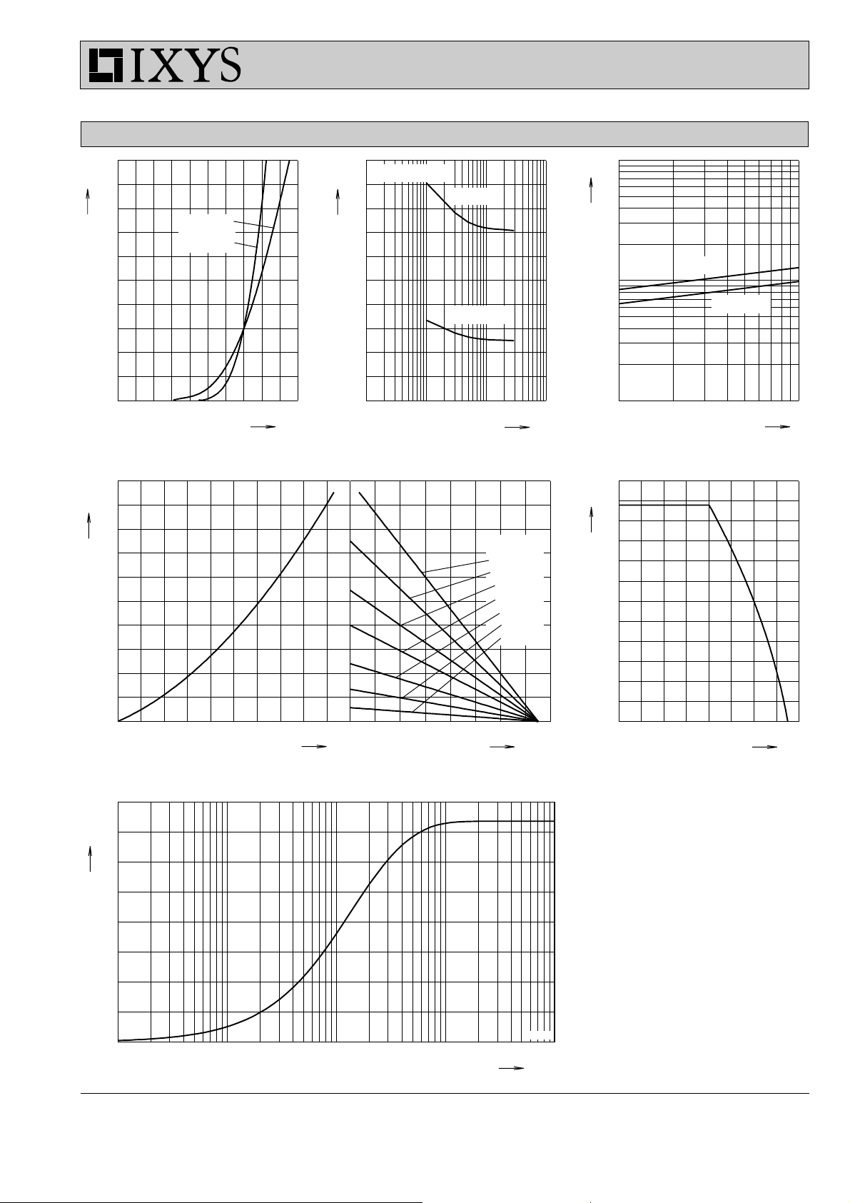
Fig. 1 Forward current versus voltage
20
0
0.001 0.01 0.1 1
s
t
Fig. 2 Surge overload current Fig. 3 I
drop per diode
500
W
400
R
P
tot
300
:
thA
0.05 K/W
0.15 K/W
0.3 K/W
0.5 K/W
1 K/W
200
2 K/W
5 K/W
100
0
0 20406080
I
d(AV)M
0 20 40 60 80 100 120 140
A
T
amb
°C °C
Fig. 4 Power dissipation versus direct output current and ambient temperature, sin
180°
1.6
1
10
23456789110
t
2
t versus time per diode
60
A
50
I
d(AV)
40
30
20
10
0
0 20406080100120140
T
C
Fig. 5 Max. forward current versus
case temperature
ms
K/W
1.2
Z
thJC
0.8
0.4
0.0
0.001 0.01 0.1 1 10
Fig. 6 Transient thermal impedance junction to case
DWFN9-16
s
t
© 2001 IXYS All rights reserved
5 - 8
Page 6
Output Inverter T1 - T6 / D1 - D6
MUBW 15-12 A7
50
V
= 17V
A
40
I
C
GE
15V
13V
30
20
10
TVJ = 25°C
0
01234567
V
CE
11V
9V
V
50
V
= 17V
A
40
I
C
GE
15V
13V
30
20
10
0
01234567
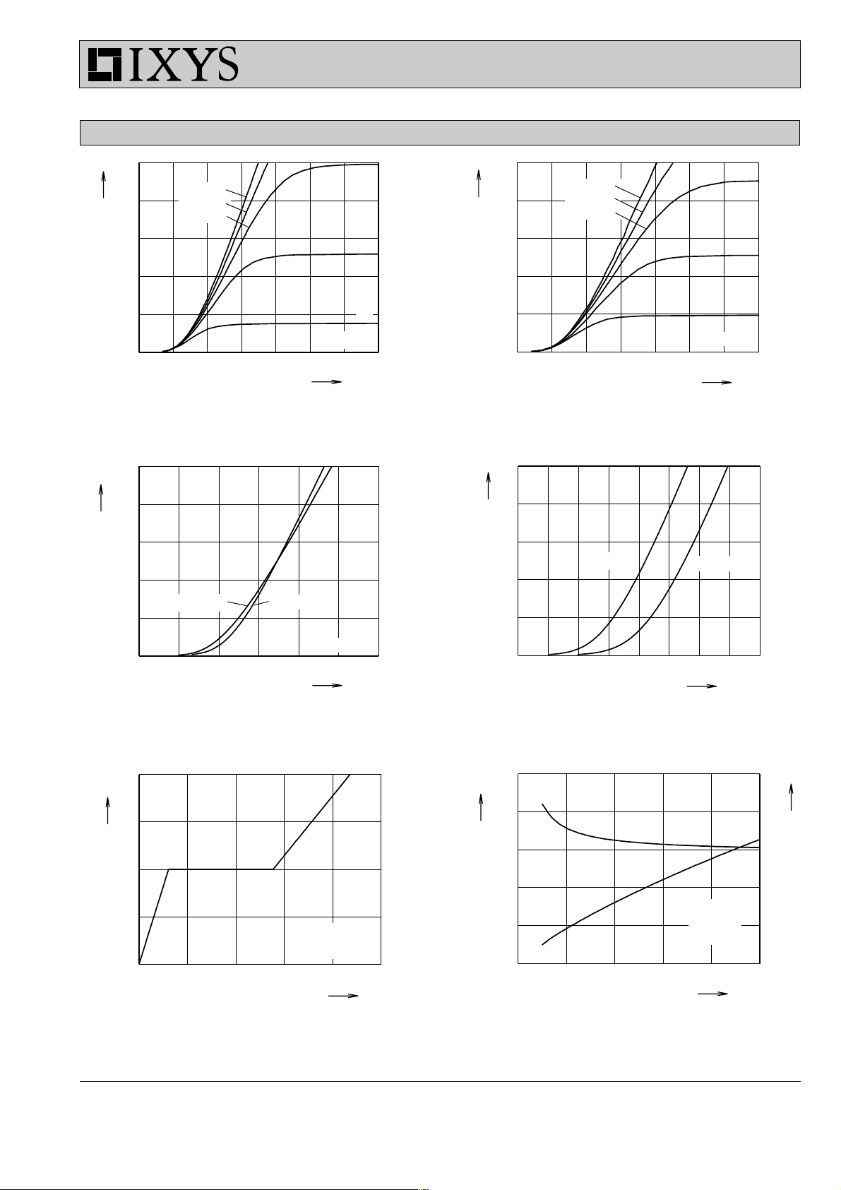
Fig. 7 Typ. output characteristics Fig. 8 Typ. output characteristics
50
A
40
I
C
30
20
T
= 125°C
VJ
TVJ = 25°C
10
50
40
A
I
F
30
20
10
V
CE
11V
9V
TVJ = 125°C
V
TVJ = 25°CTVJ = 125°C
0
VCE = 20V
4 6 8 10121416
V
GE
V
0
01234
Fig. 9 Typ. transfer characteristics Fig. 10 Typ. forward characteristics of
free wheeling diode
20
V
15
V
GE
10
5
VCE = 600V
= 15A
I
C
0
0 20406080100
Q
G
nC
50
t
rr
40
A
I
RM
30
20
10
I
RM
0
0 200 400 600 800 1000
Fig. 11 Typ. turn on gate charge Fig. 12 Typ. turn off characteristics of
free wheeling diode
V
F
-di/dt
V
TVJ = 125°C
VR = 600V
= 15A
I
F
MUBW1512A7
A/µs
$
ns
&
"
t
rr
© 2001 IXYS All rights reserved
6 - 8
Page 7
Output Inverter T1 - T6 / D1 - D6
MUBW 15-12 A7
6
mJ
J
E
on
d(on)
4
J
r
2
E
on
VCE = 600V
VGE = ±15V
R
= 82
G
T
= 125°C
VJ
0
0 102030
I
C
120
ns
t
80
40
Ω
0
A
6
mJ
E
off
4
V
2
V
R
TVJ = 125°C
0
0102030
I
C
= 600V
CE
= ±15V
GE
= 82
G
J
E
J
d(off)
off
Ω
f
600
ns
t
400
200
0
A
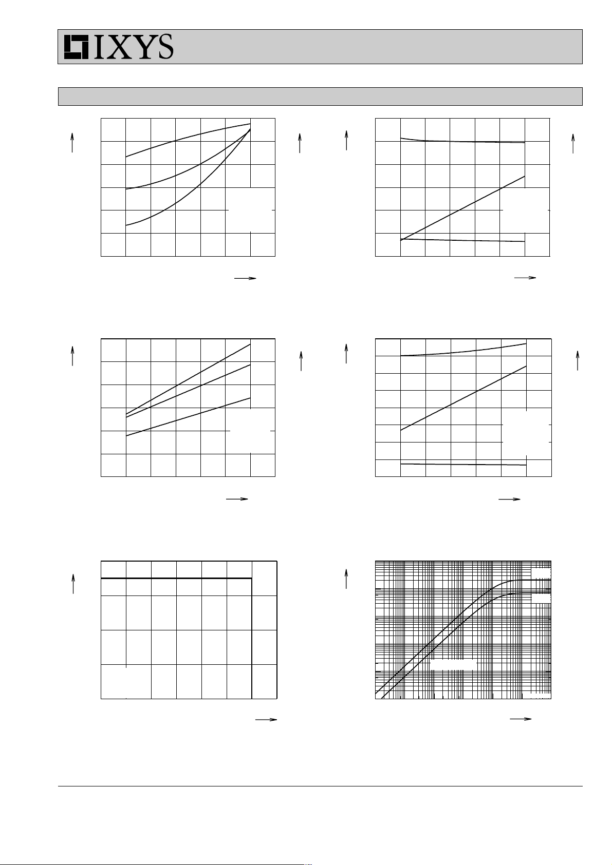
Fig. 13 Typ. turn on energy and switching Fig. 14 Typ. turn off energy and switching
times versus collector current times versus collector current
3
mJ
E
on
2
V
= 600V
CE
= ±15V
V
1
GE
IC = 15A
= 125°C
T
VJ
0
0 20406080100120140
R
G
E
J
J
on
d(on)
r
Ω
150
ns
100
50
0
t
2.0
E
mJ
E
off
1.5
1.0
0.5
off
V
V
I
C
T
0.0
0 20406080100120140
R
G
= 600V
CE
= ±15V
GE
= 15A
= 125°C
VJ
J
J
d(off)
f
Ω
800
ns
600
400
200
0
t
Fig. 15 Typ. turn on energy and switching Fig.16 Typ. turn off energy and switching
times versus gate resistor times versus gate resistor
Z
thJC
10
K/W
diode
1
IGBT
40
A
30
I
CM
0.1
20
0.01
10
RG = 82
Ω
= 125°C
T
VJ
0
0 200 400 600 800 1000 1200 1400
V
CE
0.001
0.0001
V
0.00001 0.0001 0.001 0.01 0.1 1 10
single pulse
MUBW1512A7
s
t
Fig. 17 Reverse biased safe operating area Fig. 18 Typ. transient thermal impedance
RBSOA
© 2001 IXYS All rights reserved
7 - 8
Page 8

Brake Chopper T7 / D7
MUBW 15-12 A7
30
A
25
I
C
20
TVJ = 25°C
TVJ = 125°C
15
10
5
VGE = 15V
0
0123456
V
CE
V
30
A
25
I
F
20
T
VJ
= 125°C
TVJ = 25°C
15
10
5
0
01234
V
F
V
Fig. 19 Typ. output characteristics Fig. 20 Typ. forward characteristics of
free wheeling diode
2.5
VCE = 600V
mJ
VGE = ±15V
2.0
R
= 82
E
off
1.5
1.0
G
= 125°C
T
VJ
Ω
J
d(off)
E
off
500
ns
400
300
200
1.2
E
mJ
E
t
off
0.8
off
VCE = 600V
VGE = ±15V
= 10A
I
C
TVJ = 125°C
0.4
J
d(off)
600
ns
400
200
t
0.5
0.0
0 4 8 121620
I
C
Fig. 21 Typ. turn off energy and switching Fig. 22 Typ. turn off energy and switching
times versus collector current times versus gate resistor
10
K/W
1
Z
thJC
0.1
0.01
0.001
single pulse
0.0001
0.00001 0.0001 0.001 0.01 0.1 1 10
t
Fig. 23 Typ. transient thermal impedance Fig. 24 Typ. thermistorresistance versus
J
f
A
diode
IGBT
s
100
0
10000
R
0.0
0 20 40 60 80 100 120 140
R
Temperature Sensor NTC
Ω
1000
100
0 25 50 75 100 125 150
T
temperature
G
J
f
Ω
MUBW1512A7
°C
0
© 2001 IXYS All rights reserved
8 - 8
 Loading...