

Page 1
1
Motorola TMOS Power MOSFET Transistor Device Data
Medium Power Surface Mount Products
Micro8 devices are an advanced series of power MOSFETs
which utilize Motorola’s High Cell Density HDTMOS process to
achieve lowest possible on–resistance per silicon area. They are
capable of withstanding high energy in the avalanche and commuta tion modes and the drain–to–source diode has a very low reverse
recovery time. Micro8 devices are des igned for use in low voltage,
high speed switching applications where power efficiency is important.
Typical applications are dc–dc converters, and power management in
portable and battery powered products such as computers, printers,
cellular and cordless phones. They can also be used for low voltage
motor controls in mass storage products such as disk drives and tape
drives. The avalanche energy is specified to eliminate the guesswork
in designs where inductive loads are switched and offer additional
safety margin against unexpected voltage transients.
• Miniature Micro8 Surface Mount Package — Saves Board Space
• Extremely Low Profile (<1.1 mm) for thin applications such as
PCMCIA cards
• Ultra Low R
DS(on)
Provides Higher Efficiency and Extends
Battery Life
• Logic Level Gate Drive — Can Be Driven by Logic ICs
• Diode Is Characterized for Use In Bridge Circuits
• Diode Exhibits High Speed, With Soft Recovery
• I
DSS
Specified at Elevated Temperature
• Avalanche Energy Specified
• Mounting Information for Micro8 Package Provided
DEVICE MARKING ORDERING INFORMATION
Device Reel Size Tape Width Quantity
3A
MTSF3203R2 13″ 12 mm embossed tape 4000 units
Preferred devices are Motorola recommended choices for future use and best overall value.
HDTMOS is a trademark of Motorola, Inc. TMOS is a registered trademark of Motorola, Inc. Micro8 is a registered trademark of International
Rectifier. Thermal Clad is a trademark of the Bergquist Company.
This document contains information on a product under development. Motorola reserves the right to change or discontinue this product without notice.
SEMICONDUCTOR TECHNICAL DATA
Order this document
by MTSF3203/D
Motorola, Inc. 1998
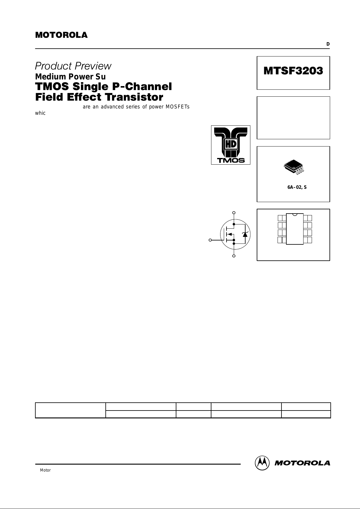
SINGLE TMOS
POWER MOSFET
4.9 AMPERES
20 VOLTS
R
DS(on)
= 0.05 OHM
CASE 846A–02, Style 1
Micro8
Motorola Preferred Device
D
S
G
Source
Source
Source
Gate
1
2
3
4
8
7
6
5
Top View
Drain
Drain
Drain
Drain
Page 2
MTSF3203
2
Motorola TMOS Power MOSFET Transistor Device Data
MAXIMUM RATINGS
(TJ = 25°C unless otherwise noted)
Rating
Symbol Max Unit
Drain–to–Source Voltage V
DSS
20 V
Drain–to–Gate Voltage (RGS = 1.0 MΩ) V
DGR
20 V
Gate–to–Source Voltage — Continuous V
GS
± 12 V
1 inch SQ.
FR–4 or G–10 PCB
Figure 1 below
Steady State
Thermal Resistance — Junction to Ambient
Total Power Dissipation @ TA = 25°C
Linear Derating Factor
Drain Current — Continuous @ TA = 25°C
Continuous @ TA = 70°C
Pulsed Drain Current
(1)
R
THJA
P
D
I
D
I
D
I
DM
70
1.79
14.29
4.9
3.9
24.4
°C/W
Watts
mW/°C
A
A
A
Minimum
FR–4 or G–10 PCB
Figure 2 below
Steady State
Thermal Resistance — Junction to Ambient
Total Power Dissipation @ TA = 25°C
Linear Derating Factor
Drain Current — Continuous @ TA = 25°C
Continuous @ TA = 70°C
Pulsed Drain Current
(1)
R
THJA
P
D
I
D
I
D
I
DM
160
0.78
6.25
3.2
2.5
16
°C/W
Watts
mW/°C
A
A
A
Operating and Storage Temperature Range TJ, T
stg
– 55 to 150 °C
Single Pulse Drain–to–Source Avalanche Energy — Starting TJ = 25°C
(VDD = 30 Vdc, VGS = 5.0 Vdc, Peak IL = 4.9 Apk, L = TBD mH, RG = 25 W)
E
AS
TBD
mJ
(1) Repetitive rating; pulse width limited by maximum junction temperature.
Figure 1. 1.0 Inch Square FR–4 or G–10 PCB Figure 2. Minimum FR–4 or G–10 PCB
Page 3
MTSF3203
3
Motorola TMOS Power MOSFET Transistor Device Data
ELECTRICAL CHARACTERISTICS (T
A
= 25°C unless otherwise noted)
Characteristic Symbol Min Typ Max Unit
OFF CHARACTERISTICS
Drain–to–Source Breakdown Voltage (Cpk ≥ 2.0) (1) (3)
(VGS = 0 Vdc, ID = 250 µAdc)
T emperature Coef ficient (Positive)
V
(BR)DSS
20
—
—
TBD
—
—
Vdc
mV/°C
Zero Gate Voltage Drain Current
(VDS = 20 Vdc, VGS = 0 Vdc)
(VDS = 20 Vdc, VGS = 0 Vdc, TJ = 125°C)
I
DSS
—
—
—
—
1.0
25
µAdc
Gate–Body Leakage Current (VGS = ± 12 Vdc, VDS = 0) I
GSS
— — 100 nAdc
ON CHARACTERISTICS
(1)
Gate Threshold Voltage (Cpk ≥ 2.0) (3)
(VDS = VGS, ID = 250 µAdc)
Threshold Temperature Coefficient (Negative)
V
GS(th)
1.0
—
TBD
TBD
—
—
Vdc
mV/°C
Static Drain–to–Source On–Resistance (Cpk ≥ 2.0) (3)
(VGS = 4.5 Vdc, ID = 4.9 Adc)
(VGS = 2.5 Vdc, ID = 3.9 Adc)
R
DS(on)
—
—
TBD
TBD
40
50
mΩ
Forward Transconductance (VDS = 10 Vdc, ID = 4.9 Adc) g
FS
2.0 — — Mhos
DYNAMIC CHARACTERISTICS
Input Capacitance
C
iss
— TBD — pF
Output Capacitance
(VDS = 16 Vdc, VGS = 0 Vdc,
f = 1.0 MHz
)
C
oss
— TBD —
Transfer Capacitance
f = 1.0 MHz)
C
rss
— TBD —
SWITCHING CHARACTERISTICS
(2)
Turn–On Delay Time
t
d(on)
— TBD — ns
Rise Time
(VDS = 10 Vdc, ID = 4.9 Adc,
t
r
— TBD —
Turn–Off Delay Time
(
DS
,
D
,
VGS = 4.5 Vdc, RG = 6 Ω) (1)
t
d(off)
— TBD —
Fall Time t
f
— TBD —
Turn–On Delay Time
t
d(on)
— TBD — ns
Rise Time
(VDD = 10 Vdc, ID = 3.9 Adc,
t
r
— TBD —
Turn–Off Delay Time
(
DD
,
D
,
VGS = 2.5 Vdc, RG = 6 Ω) (1)
t
d(off)
— TBD —
Fall Time t
f
— TBD —
Gate Charge
Q
T
— TBD TBD nC
(VDS = 10 Vdc, ID = 4.9 Adc,
Q
1
— TBD —
(
DS
,
D
,
VGS = 4.5 Vdc)
Q
2
— TBD —
Q
3
— TBD —
SOURCE–DRAIN DIODE CHARACTERISTICS
Forward On–Voltage
(IS = 1.5 Adc, VGS = 0 Vdc) (1)
(IS = 1.5 Adc, VGS = 0 Vdc, TJ = 125°C)
V
SD
—
—
TBD
TBD
1.0
—
Vdc
Reverse Recovery Time
t
rr
— TBD —
ns
(IS = 1.5 Adc, VGS = 0 Vdc,
dI
/dt = 100 A/µs) (1
)
t
a
— TBD —
dIS/dt = 100 A/µs)
(1)
t
b
— TBD —
Reverse Recovery Storage Charge Q
RR
— TBD — µC
(1) Pulse Test: Pulse Width ≤300 µs, Duty Cycle ≤ 2%.
(2) Switching characteristics are independent of operating junction temperature.
(3) Reflects typical values.
Cpk =
Max limit – Typ
3 x SIGMA
Page 4

MTSF3203
4
Motorola TMOS Power MOSFET Transistor Device Data
INFORMATION FOR USING THE Micro8 SURFACE MOUNT PACKAGE
MINIMUM RECOMMENDED FOOTPRINT FOR SURFACE MOUNTED APPLICATIONS
Surface mount board layout is a critical portion of the total
design. The footprint for the semiconductor packages must be
the correct size to ensure proper solder connection interface
between the board and the package. With the correct pad
geometry, the packages will self–align when subjected to a
solder reflow process.
mm
inches
0.041
1.04
0.208
5.28
0.015
0.38
0.0256
0.65
0.126
3.20
Micro8 POWER DISSIP ATION
The power dissipation of the Micro8 is a function of the input
pad size. This can vary from the minimum pad size for
soldering to the pad size given for maximum power
dissipation. Power dissipation for a surface mount device is
determined by T
J(max)
, the maximum rated junction
temperature of the die, R
θJA
, the thermal resistance from the
device junction to ambient; and the operating temperature, TA.
Using the values provided on the data sheet for the Micro8
package, PD can be calculated as follows:
PD =
T
J(max)
– T
A
R
θJA
The values for the equation are found in the maximum
ratings table on the data sheet. Substituting these values into
the equation for an ambient temperature TA of 25°C, one can
calculate the power dissipation of the device which in this case
is 0.78 Watts.
PD =
150°C – 25°C
160°C/W
= 0.78 Watts
The 160°C/W for the Micro8 package assumes the
recommended footprint on a glass epoxy printed circuit board
to achieve a power dissipation of 0.78 Watts using the footprint
shown. Another alternative would be to use a ceramic
substrate or an aluminum core board such as Thermal Clad.
Using board material such as Thermal Clad, the power
dissipation can be doubled using the same footprint.
SOLDERING PRECAUTIONS
The melting temperature of solder is higher than the rated
temperature of the device. When the entire device is heated
to a high temperature, failure to complete soldering within a
short time could result in device failure. Therefore, the
following items should always be observed in order to
minimize the thermal stress to which the devices are
subjected.
• Always preheat the device.
• The delta temperature between the preheat and soldering
should be 100°C or less.*
• When preheating and soldering, the temperature of the
leads and the case must not exceed the maximum
temperature ratings as shown on the data sheet. When
using infrared heating with the reflow soldering method,
the difference shall be a maximum of 10°C.
• The soldering temperature and time shall not exceed
260°C for more than 10 seconds.
• When shifting from preheating to soldering, the maximum
temperature gradient shall be 5°C or less.
• After soldering has been completed, the device should be
allowed to cool naturally for at least three minutes.
Gradual cooling should be used as the use of forced
cooling will increase the temperature gradient and result
in latent failure due to mechanical stress.
• Mechanical stress or shock should not be applied during
cooling.
* Soldering a device without preheating can cause excessive
thermal shock and stress which can result in damage to the
device.
Page 5

MTSF3203
5
Motorola TMOS Power MOSFET Transistor Device Data
TYPICAL SOLDER HEATING PROFILE
For any given circuit board, there will be a group of control
settings that will give the desired heat pattern. The operator
must set temperatures for several heating zones and a figure
for belt speed. T aken together , these control settings make up
a heating “profile” for that particular circuit board. On
machines controlled by a computer, the computer remembers
these profiles from one operating session to the next. Figure
3 shows a typical heating profile for use when soldering a
surface mount device to a printed circuit board. This profile will
vary among soldering systems, but it is a good starting point.
Factors that can affect the profile include the type of soldering
system in use, density and types of components on the board,
type of solder used, and the type of board or substrate material
being used. This profile shows temperature versus time. The
line on the graph shows the actual temperature that might be
experienced on the surface of a test board at or near a central
solder joint. The two profiles are based on a high density and
a low density board. The Vitronics SMD310 convection/infrared reflow soldering system was used to generate this
profile. The type of solder used was 62/36/2 Tin Lead Silver
with a melting point between 177–189°C. When this type of
furnace is used for solder reflow work, the circuit boards and
solder joints tend to heat first. The components on the board
are then heated by conduction. The circuit board, because it
has a large surface area, absorbs the thermal energy more
efficiently, then distributes this energy to the components.
Because of this effect, the main body of a component may be
up to 30 degrees cooler than the adjacent solder joints.
STEP 1
PREHEAT
ZONE 1
“RAMP”
STEP 2
VENT
“SOAK”
STEP 3
HEATING
ZONES 2 & 5
“RAMP”
STEP 4
HEATING
ZONES 3 & 6
“SOAK”
STEP 5
HEATING
ZONES 4 & 7
“SPIKE”
STEP 6
VENT
STEP 7
COOLING
200
°
C
150
°
C
100
°
C
50°C
TIME (3 TO 7 MINUTES TOTAL)
T
MAX
SOLDER IS LIQUID FOR
40 TO 80 SECONDS
(DEPENDING ON
MASS OF ASSEMBLY)
205
°
TO 219°C
PEAK AT
SOLDER JOINT
DESIRED CURVE FOR LOW
MASS ASSEMBLIES
100°C
150°C
160
°
C
170°C
140
°
C
Figure 3. Typical Solder Heating Profile
DESIRED CURVE FOR HIGH
MASS ASSEMBLIES
Page 6

MTSF3203
6
Motorola TMOS Power MOSFET Transistor Device Data
T APE & REEL INFORMA TION
Micro8
Dimensions are shown in millimeters (inches)
FEED DIRECTION
SECTION A–A
NOTES:
1. CONFORMS TO EIA–481–1.
2. CONTROLLING DIMENSION: MILLIMETER.
PIN
NUMBER 1
NOTES:
1. CONFORMS TO EIA–481–1.
2. CONTROLLING DIMENSION: MILLIMETER.
3. INCLUDES FLANGE DISTORTION AT OUTER EDGE.
4. DIMENSION MEASURED AT INNER HUB.
12.30
4.10 (.161)
11.70
(.484)
(.461)
1.85 (.072)
3.90 (.154)
2.05 (.080)
1.95 (.077)
BBA
A
8.10 (.318)
7.90 (.312)
5.55 (.218)
5.45 (.215)
1.65 (.065)
1.60 (.063)
1.50 (.059)
1.60 (.063)
1.50 (.059)
TYP.
0.35 (.013)
0.25 (.010)
3.50 (.137)
3.30 (.130)
1.50 (.059)
1.30 (.052)
SECTION B–B
5.40 (.212)
5.20 (.205)
330.0
(13.20)
MAX.
50.0
(1.97)
MIN.
14.4 (.57)
12.4 (.49)
NOTE 4
18.4 (.724)
MAX.
NOTE 3
13.2 (.52)
12.8 (.50)
Page 7

MTSF3203
7
Motorola TMOS Power MOSFET Transistor Device Data
P ACKAGE DIMENSIONS
STYLE 1:
PIN 1. SOURCE
2. SOURCE
3. SOURCE
4. GATE
5. DRAIN
6. DRAIN
7. DRAIN
8. DRAIN
CASE 846A–02
ISSUE D
MICRO8
S
B
M
0.08 (0.003) A
S
T
DIM MIN MAX MIN MAX
INCHESMILLIMETERS
A 2.90 3.10 0.114 0.122
B 2.90 3.10 0.114 0.122
C ––– 1.10 ––– 0.043
D 0.25 0.40 0.010 0.016
G 0.65 BSC 0.026 BSC
H 0.05 0.15 0.002 0.006
J 0.13 0.23 0.005 0.009
K 4.75 5.05 0.187 0.199
L 0.40 0.70 0.016 0.028
NOTES:
1. DIMENSIONING AND TOLERANCING PER ANSI
Y14.5M, 1982.
2. CONTROLLING DIMENSION: MILLIMETER.
3. DIMENSION A DOES NOT INCLUDE MOLD FLASH,
PROTRUSIONS OR GATE BURRS. MOLD FLASH,
PROTRUSIONS OR GATE BURRS SHALL NOT
EXCEED 0.15 (0.006) PER SIDE.
4. DIMENSION B DOES NOT INCLUDE INTERLEAD
FLASH OR PROTRUSION. INTERLEAD FLASH OR
PROTRUSION SHALL NOT EXCEED 0.25 (0.010)
PER SIDE.
–B–
–A–
D
K
G
PIN 1 ID
8 PL
0.038 (0.0015)
–T–
SEATING
PLANE
C
H
J
L
Page 8

MTSF3203
8
Motorola TMOS Power MOSFET Transistor Device Data
Motorola reserves the right to make changes without further notice to any products herein. Motorola makes no warranty , representation or guarantee regarding
the suitability of its products for any particular purpose, nor does Motorola assume any liability arising out of the application or use of any product or circuit, and
specifically disclaims any and all liability, including without limitation consequential or incidental damages. “T ypical” parameters which may be provided in Motorola
data sheets and/or specifications can and do vary in different applications and actual performance may vary over time. All operating parameters, including “Typicals”
must be validated for each customer application by customer’s technical experts. Motorola does not convey any license under its patent rights nor the rights of
others. Motorola products are not designed, intended, or authorized for use as components in systems intended for surgical implant into the body, or other
applications intended to support or sustain life, or for any other application in which the failure of the Motorola product could create a situation where personal injury
or death may occur. Should Buyer purchase or use Motorola products for any such unintended or unauthorized application, Buyer shall indemnify and hold Motorola
and its officers, employees, subsidiaries, affiliates, and distributors harmless against all claims, costs, damages, and expenses, and reasonable attorney fees
arising out of, directly or indirectly, any claim of personal injury or death associated with such unintended or unauthorized use, even if such claim alleges that
Motorola was negligent regarding the design or manufacture of the part. Motorola and are registered trademarks of Motorola, Inc. Motorola, Inc. is an Equal
Opportunity/Affirmative Action Employer.
Mfax is a trademark of Motorola, Inc.
How to reach us:
USA/EUROPE /Locations Not Listed: Motorola Literature Distribution; JAPAN: Nippon Motorola Ltd.: SPD, Strategic Planning Office, 141,
P.O. Box 5405, Denver, Colorado 80217. 1–303–675–2140 or 1–800–441–2447 4–32–1 Nishi–Gotanda, Shagawa–ku, Tokyo, Japan. 03–5487–8488
Customer Focus Center: 1–800–521–6274
Mfax: RMFAX0@email.sps.mot.com – TOUCHTONE 1–602–244–6609 ASIA/PACIFIC: Motorola Semiconductors H.K. Ltd.; 8B Tai Ping Industrial Park,
Moto rola Fax Back Syste m – US & Canada ONLY 1–800–774–1848 51 Ting Kok Road, Tai Po, N.T., Hong Kong. 852–26629298
– http://sps.motorola.com/mfax/
HOME PAGE: http://motorola.com/sps/
MTSF3203/D
◊
 Loading...