

Page 1
ISO-CMOS
MT093
8 x 12 Analog Switch Array
Features
• Internal cont rol lat ches and add ress d eco der
• Short set-up and hold times
• Wide ope rating v oltag e: 4. 5V to 14.5V
• 3.5Vpp an alog sign al capability
•R
• ∆R
65Ω max. @ VDD=14V, 25°C
ON
≤ 10Ω @ VDD=14V, 25°C
ON
• Full CMOS switch for low distortion
• Minimum f eedthr oug h and c ros stal k
• Low power consumption ISO-CMOS technology
Applications
• PBX systems
• Mobile rad io
• Test equipment /instru men tatio n
• Analo g/ di gita l m ult ip le xers
• Audio/Video switching
ISSUE 1 January 1990
Ordering Information
MT093AC 40 Pin Ceramic DIP
MT093AE 40 Pin Plastic DIP
MT093AP 44 Pin PLCC
0° to 70°C
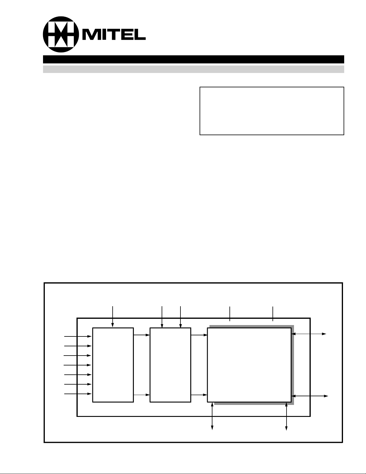
Description
The Mitel MT093 is fabricated in MITEL’s ISO-CMOS
technology providing low power dissipation and high
reliability. The device contains a 8×12 array of
crosspoint switches along with a 7 to 96 line decoder
and latch circuits. Any one of the 96 switches can be
addressed by selecting the appropriate seven input
bits. The selected switch can be turned on or off by
applying a logical one or zero to the DATA input.
AX0
AX1
AX2
AX3
AY0
AY1
AY2
STROBE DATA RESET VDD VSS
11
8 x 12
7 to 96
Decoder
Latches
Switch
Array
9696
• • • • • • • • • • • • • • • • • • •
Yi I/O (i=0-7)
Figure 1 - Functional Block Diagram
• • • • • • • • • • • • • • • •
Xi I/O
(i=0-11)
3-65
Page 2
MT093 ISO-CMOS
1
Y3
AY2
RESET
AX3
AX0
X10
X11
STROBE
VSS
2
3
4
5
6
NC
7
NC
8
X6
9
X7
10
X8
11
X9
12
13
14
NC
15
Y7
16
NC
17
Y6
18
19
Y5
20
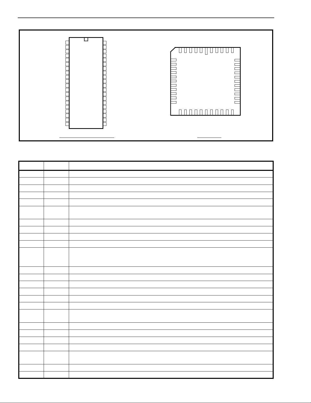
40 PIN CERDIP/PLASTIC DIP 44 PIN PLCC
40
39
38
37
36
35
34
33
32
31
30
29
28
27
26
25
24
23
22
21
VDD
Y2
DATA
Y1
NC
Y0
NC
X0
X1
X2
X3
X4
X5
NC
NC
AY1
AY0
AX2
AX1
Y4
NC
NC
X6
XY
X8
X9
X10
X11
NC
NC
NC
DATA
Y2
VDD
Y3
AY2
RESET
AX3
AX0
NC
65432 44434241
7
8
9
10
11
12
13
14
15
16
17
Y7
Y6
1
23181920 2122 2425262728
Y5
VSS
STROBE
Y4
AX1
AX2
AY0
Y1
40
39
38
37
36
35
34
33
32
31
30
29
AY1
Y0
NC
NC
X0
X1
X2
X3
X4
X5
NC
NC
NC
NC
Figure 2 - Pin Connections
Pin Description
Pin #* Name Description
1Y3Y3 Analog (Input/Output): this is connected to the Y3 column of the switch array.
2AY2Y2 Add ress Lin e (Inp ut).
3 RESET Master RESET (Input): this is used to turn off all switches. Active High.
4,5 AX3,AX0 X3 and X0 Address Lines (Inputs).
6,7 NC No Connection.
8-13 X6-X11 X6-X11 Analog (Inputs/Outputs): these are connected to the X6-X11 rows of the switch
array.
14 NC No Connection.
15 Y7 Y7 Analog (Input/Output): this is connected to the Y7 column of the switch array.
16 NC No Connection.
17 Y6 Y6 Analog (Input/Output): this is connected to the Y6 column of the switch array.
18 STROB E STROBE (Input): enables function selected by address and data. Address must be stable
before STRO BE goes high and DATA must be stable on the falling edge of the STROBE .
Active High.
19 Y5 Y5 Analog (Input/Output): this is connected to the Y5 column of the switch array.
20 V
21 Y4 Y4 Analog (Input/Output): this is connected to the Y4 column of the switch array.
22, 23 AX1,AX2 X1 and X2 Address Lines (Inputs).
24, 25 AY0,AY1 Y0 and Y1 Address Lines (Inputs).
26, 27 NC No Connection.
28 - 33 X5-X0 X5-X0 Analog (Inputs/ Ou tputs): these are connected to the X5-X0 rows of the switch
34 NC No Connection.
35 Y0 Y0 Analog (Input/Ou tpu t): this is connected to the Y0 column of the switch array.
36 NC No Connection.
37 Y1 Y1 Analog (Input/Ou tpu t): this is connected to the Y1 column of the switch array.
38 DATA DATA (Input): a logic high input will turn on the selected switch and a logic low will turn off
39 Y2 Y2 Analog (Input/Ou tpu t): this is connected to the Y2 column of the switch array.
40 V
* Plastic DIP and CERDIP only.
Ground Reference.
SS
array.
the selected switch. Active High.
Positive Pow er Supp ly.
DD
3-66
Page 3

ISO-CMOS MT093
Functional Description
The MT093 is an analog switch matrix with an array
size of 8 x 12. The switch array is arranged such that
there are 8 columns by 12 rows. The columns are
referred to as the Y input/output lines and the rows
are the X input/output lines. The crosspoint analog
switch array will interconnect any X line with any Y
line when turned on and provide a high degree of
isolation when turned off. The control memory
consists of a 96 bit write only RAM in which the bits
are selected by the address input lines (AY0-AY2,
AX0-AX3) . Data is presented to the memory on the
DATA input line. Data is asynchronously written into
memory whenever the STROBE input is high and is
latched on the falling edge of STROBE. A logical “1”
written into a memory cell turns the corresponding
crosspoint switch on and a logical “0” turns the
crosspoint off. Only the crosspoint switches
corresponding to the addressed memory location are
altered when data is written into memory. The
remaining switches retain their previous states. Any
combination of X and Y lines can be interconnected
by establishing appropriate patterns in the control
memory. A logical “1” on the RESET input line will
asynchronously return all memory locations to logical
“0” turnin g off al l cr o ssp oi n t s witches.
Address Decode
The seven address lines along with the STROBE
input are logically ANDed to form an enable signal
for the resettable transparent latches. The DATA
input is buffered and is used as the input to all
latches. To write to a location, RESET mu st be low
while the address and data lines are set up. Then the
STROBE input is set high and then low causing the
data to be latched. The data can be changed while
STROBE is high, however, the corresponding switch
will turn on and off in accordance with the data. Data
must be stable on the falling edge of STROBE in
order for corr e ct da ta to be writ te n t o th e l atc h .
3-67
Page 4

MT093 ISO-CMOS
Absolute Maximum Ratings*- Voltages are with respect to V
unless otherwise stated.
SS
Parameter Symbol Min Max Units
1 Supply Voltage V
2 Analog Input Voltage V
3 Digital Input Voltage V
DD
V
SS
INA
IN
-0.3
-0.3
V
16.0
DD
+0.3
-0.3 VDD+0.3 V
VSS-0.3 VDD+0.3 V
4 Current on any I/O Pin I ±15 mA
5 Storage Tem perature T
6 Package Power Dissipation PLASTIC DIP
CERDIP
* Exceeding these values may cause permanent damage. Functional operation under these conditions is not implied.
Recommended Operating Conditions - Voltages are with respect to V
S
P
D
P
D
SS
-65 +150 °C
0.6
1.0
unless otherwise stated.
Characteris tics Sym Min Typ Max Units Test Conditions
1 Operating Temperature T
2 Supply Voltage V
3 Analog In put Voltage V
4 Digital In put Voltage V
DC Electrical Characteristics
†
Characteristics Sym Min Typ
O
DD
INA
IN
- Voltages are with respect to V
025 70 °C
4.5 14.5 V
V
SS
V
SS
‡
3.5 V
SS
V
DD
=0V, V
DD
V
=14V unless otherwi se stated .
Max Units Test Conditio ns
V
V
W
W
1 Quiescent Supply Current I
DDQ
1100µA All digital inputs at VIN=VSS or
V
DD
7 15 mA A ll digi tal i np uts at VIN=2.4V
2 Off-state Leakage Current I
3 Input Logic “0” level V
4 Input Logic “1” level V
5 Input Leakage (digital pins) I
† DC Electrical Characteristics are over recommended temperature range & recommended power supply voltages.
‡ Typical figures are at 25°C and are for design aid only; not guaran teed and no t subject to producti on testing .
OFF
IL
IH
LEAK
2.4 V
DC Electrical Characteristics- Switch Resistance - V
±1 µAIVXi - VYjI = VDD - V
0.8 V
10 µA All digital inp uts at VIN = VSS
or V
DD
IDC/VODC
I/O pins.
is the external DC offset applied at the analog
Characteristics Sym 25°C 60°C 70°C Un its Test Condi tio ns
Typ Max Typ Max Typ Max
1 On-state V
Resistance
2 Difference in on-state
resistance between two
switches
DD
=14V
R
∆R
45 65 75 Ω VSS=0V,
ON
510 10 10 ΩVDD=14V, VSS=0,
ON
IV
V
V
V
V
IV
IDC
ODC
IDC
ODC
Xi-VYj
Xi-VYj
SS
I = 0.25V
=6.75V
=6.5V
=6.75V
=6.5V
I = 0.25V
3-68
Page 5

ISO-CMOS MT093
AC Electrical Characteristics† - Crosspoint Performance-V
I/O pins. Voltages are with respect to V
=7V, VDC=0V, VSS=-7V, unless otherwise stated.
DD
is the external DC offset applied at the analog
DC
Characteristics Sym Min Typ‡Max Units Te s t Co nditions
1 Switch I/O Capacitance C
2 Feedthrough Capacitance C
3 Frequency Response
F
Channel “ON”
20LOG(V
OUT/VXi
)=-3dB
S
F
3dB
20 pF f=1 MH z
0.2 pF f=1 MH z
45 MHz Switch is “ON”; V
sinewave; R
= 1kΩ
L
4 Total Harmonic Distortion THD 0.05 % Switch is “ON”; V
sinewave f= 1k Hz; R
5 Feedthrough
Channel “OFF”
Feed.=20LOG (V
OUT/VXi
)
6 Crosstalk between any two
channels for switches Xi-Yi and
Xj-Yj .
Xtalk=20LOG (V
Yj/VXi
).
7 Propagation delay throu gh
FDT -95 dB All Switches “OFF”; V
2Vpp sinewave f= 1kHz;
R
= 1kΩ.
L
X
talk
t
PS
-45 dB V
-90 dB V
-85 dB V
-80 dB V
50 ns RL=1kΩ; CL=50pF
=2Vpp sinewave
INA
f= 10MHz; R
=2Vpp sinewave
INA
f= 10kHz; R
=2Vpp sinewave
INA
f= 10kHz; R
=2Vpp sinewave
INA
f= 1kHz; R
L
= 75Ω.
L
= 600Ω.
L
= 1kΩ.
L
= 10kΩ.
switc h
† Timing is over recommended temperature range.
‡ Typical figures are at 25°C and are for design aid only; not guaranteed and not subject to producti on testin g.
Crosstal k m ea su r em e nts a re fo r Pl as tic D I PS o nl y, cross tal k va lu es f or PLCC pa c kag e s a re ap proximat el y 5 d B b ett er.
AC Electrical Characteristics† - Control and I/O Timings- V
I/O pins. Voltages are with respect to V
=7V, VDC=0V, VSS=-7V, unless otherwise stated.
DD
is the external DC offset applied at the an alog
DC
Characteristics Sym Min Typ‡Max Units Test Conditions
= 2Vpp
INA
= 2Vpp
INA
L
=1kΩ
=
INA
1 Control Input crosstalk to switch
(for DATA, STROBE, Address)
2 Digit al Input Capa citan ce C
3 Switching Frequency F
4 Se tup Time DATA to STRO BE t
5 Hold Time DATA to STROBE t
6 Setup Time Address to STROBE t
7 Hold Time Address to STROBE t
8 STROBE Pulse Width t
9 RES ET P ulse Widt h t
10 STROBE to Switch Status Delay t
11 DATA to Swit ch Status Delay t
12 RESET to Switch Status Delay t
† Timing is over recommended temperature range.
Digital Inp ut ris e tim e (t r) an d fall tim e (tf) = 10ns.
‡ Typical figures are at 25°C and are for design aid only; not guaran teed and no t subject to producti on testing .
CX
SPW
RPW
DS
DH
AS
AH
S
D
R
talk
DI
O
50 mVpp VIN=3V+VDC squarewave;
R
IN
10 pF f=1MHz
10 MHz
20 ns RL= 1kΩ, CL=50pF
20 ns RL= 1kΩ, CL=50pF
20 ns RL= 1kΩ, CL=50pF
20 ns RL= 1kΩ, CL=50pF
40 ns RL= 1kΩ, CL=50pF
80 ns RL= 1kΩ, CL=50pF
80 200 ns RL= 1kΩ, CL=50pF
100 200 ns RL= 1kΩ, CL=50pF
70 200 ns RL= 1kΩ, CL=50pF
=1kΩ, RL=10kΩ.
3-69
Page 6

MT093 ISO-CMOS
t
RPW
RESET
STROBE
ADDRESS
DATA
SWITCH
ON
t
SPW
t
AS
50% 50%
50% 50%
t
DS
t
DH
t
AH
50% 50%
50%50%50%
OFF
t
D
t
S
t
R
Figure 3 - Control Memory Timing Diagram
AX0 AX1 AX2 AX3 AY 0 AY1 AY2 Connect ion
0
1
0
1
0
1
0
1
0
1
0
1
0
1
0
1
0
↓
1
0
↓
1
0
↓
1
0
↓
1
0
↓
1
0
↓
1
0
↓
1
➀
This add r es s ha s no e ffec t o n d ev ic e s tat us .
0
0
1
1
0
0
1
1
0
0
1
1
0
0
1
1
0
↓
0
0
↓
0
0
↓
0
0
↓
0
0
↓
0
0
↓
0
0
↓
0
0
0
0
0
1
1
1
1
0
0
0
0
1
1
1
1
0
↓
1
0
↓
1
0
↓
1
0
↓
1
0
↓
1
0
↓
1
0
↓
1
0
0
0
0
0
0
0
0
1
1
1
1
1
1
1
1
0
↓
1
0
↓
1
0
↓
1
0
↓
1
0
↓
1
0
↓
1
0
↓
1
0
0
0
0
0
0
0
0
0
0
0
0
0
0
0
0
1
↓
1
0
↓
0
1
↓
1
0
↓
0
1
↓
1
0
↓
0
1
↓
1
0
0
0
0
0
0
0
0
0
0
0
0
0
0
0
0
0
↓
0
1
↓
1
1
↓
1
0
↓
0
0
↓
0
1
↓
1
1
↓
1
Table 1. Address Decode Truth Table
0
0
0
0
0
0
0
0
0
0
0
0
0
0
0
0
0
↓
0
0
↓
0
0
↓
0
1
↓
1
1
↓
1
1
↓
1
1
↓
1
No Connection
No Connection
No Connection
No Connection
X0-Y0
X1-Y0
X2-Y0
X3-Y0
X4-Y0
X5-Y0
X6-Y0
X7-Y0
X8-Y0
X9-Y0
X10-Y0
X11-Y0
X0-Y1
↓ ↓
X11-Y1
X0-Y2
↓ ↓
X11-Y2
X0-Y3
↓ ↓
X11-Y3
X0-Y4
↓ ↓
X11-Y4
X0-Y5
↓ ↓
X11-Y5
X0-Y6
↓ ↓
X11-Y6
X0-Y7
↓ ↓
X11-Y7
t
R
➀
➀
➀
➀
3-70
 Loading...