

Page 1

June 2002
Revised April 2003
MSX532
532 Port Digital Crosspoint Switch with LVTTL I/O’s
MSX532 532 Port Digital Crosspoint Switch with LVTTL I/O’s
General Description
The MSX family of SRAM-based bit-oriented switching
devices offer flow-through NRZ data rates of up to 150Mb/s
and registered clo ck frequencies of up to 75MHz. Th e I/O
buffers are individually configurable. The I/O buffers can be
connected to each othe r through the switch matrix, which
supports One-to-One and One-to-Many connections.
The proprietary Ra pidConfigure
fast configuration of both the I/O buffers and switch mat rix.
It also allows readback of the device for test and verification purposes. The MSX devices also support the industry
standard JTAG (IEEE 1149.1) interface for boundary scan
testing. The JTAG interface can also be used t o downlo ad
configuration data to the device. A functional block diagram
of the MSX architecture is shown in Figure 1.
parallel interface allows
Features
■ SRAM-based, in-system programmable
■ Configurable I/O Ports
• Individually programmable as input, output,
bi-directional, or Bus Repeater
• Control Signals per I/O por t: 2 input enables, 2 output
enables, 2 Global Clock inputs and Next Neighbor
Clock option
• Output data inversion: capable of inverting output
signals in flow through mode
■ Non-blocking switch matrix
• One-to-One and One-to-Many connections
Double-buffered configuration RAM cells for
simultaneous global updates
■ Registered and flow-through data modes
• Up to 75 MHz clock frequency in registered mode
• Up to 150 Mb/s in flow-through mode
■ 20 ns propagation delay in flow-through mode
■ 8 mA output current
■ Dedicated RapidConfigure parallel interface or JTAG
serial interface avail able for configur ation and r eadback
of MSX devices
■ 3.3V operation, LVTTL I/O's (5V tolerant)
■ MSX532 is offered in a 792 TBGA package
mode
Applications
• Telecom and dataco m sw itching
• Video switches and servers
• Test equipm ent
Ordering Code:
Order Number Package Number Package Description
MSX532TB792 BGA792A 792-Ball Thermally-Enhanced Ball Grid Array (TBGA), JEDEC MO-149, 1.0mm pitch,
MSX, Bus Repeater, and RapidConfigure are trademarks of Fairchild Semiconductor Corporation.
© 2003 Fairchild Semiconductor Corporation DS500746 www.fairchildsemi.com
40mm Square
Page 2

MSX532
FIGURE 1. MSX 532 Functional Block Diagram
Introduction
Switch Matrix
The MSX family are SRAM-based, bit-oriented switching
devices. The main functional block of the device is a Switch
Matrix as shown in Figure 1. The Switch Matrix is an x-y
routing structur e (or grid). Each horizontal signa l trace is
hardwired to a corresponding vertical signal trace as
shown by the junction dots. An I/O Port pin connects to this
horizontal-vertical trace pair through a programmable
buffer. Signal paths through the Sw itch Matr ix ar e well ba lanced, resulting in predictable and uniform pin-to-pin
delays.
The two SRAM c ells (shown in Figure 2) are a rranged so
that a double buffered scheme can be employed. The
Active SRAM cells are responsible for establishing connections in the switch mat rix by turning ON a pass tra nsistor,
while the Loadin g SRAM cell can be used to stor e a second configuration that can be transferred to the Active
SRAM cell at any time. If the UPDATE signal is asserted
HIGH, the contents o f the Loading SRAM cell ar e transferred to the Active SRAM cell an d the switch matrix connection is either made or broken.
The UPDATE signal can be used to control when the
switch matrix is re configured. Fo r instance, a s long as the
UPDATE signal is de-asserted (held LOW), the Loading
SRAM cells for the e ntire switch matr ix could be changed
www.fairchildsemi.com 2
without affecting the current configuration of the switch.
When the UPDATE signal is asserted HIGH, the entire
switch matrix would be reconfigured simultaneously. If the
UPDATE signal is asserted continuously, all crosspoint programming commands (generated by JTAG or RapidConfigure programming cycles) will take effect immediately, since
the Loading SRAM cell’s contents will be transferred
directly to the Active SRAM cell.
FIGURE 2. MSX Switch Matrix Diagram
Page 3

Introduction (Continued)
Input and Output Buffers (I/O buffers)
Each signal in the switch matrix is connected to a programmable I/O buffer, which is independently configured
through either the Ra pidConfigure o r JTAG Interface. The
I/O buffer attributes inc lude its signa l direction (input, output or bi-directional) and data flow mode (flow-th rough or
registered). The signa l can also be invert ed at the output.
Trickle current source (normally 15
µA) on the pin side and
V
DD
{
IE
CLK
{
Sources
Next
Neighbor
CLK_IN
MSX532
array side for each I/ O Port and contr ol pin is used t o pull
unused or non-driven circuits to a stable HIGH level. Figure
3 shows a basic block diagram of an I/O buffer with the
sources for the three control signals (IE, OE an d CLK ). For
any given port num ber, these three control sig nals can be
selected from one of two sour ces. The control signals are
explained in more detail in the following section.
IN
I/O
Port
CLK
Sources
Next
Neighbor
OE
CLK_OUT
{
{
V
SS
FIGURE 3. MSX I/O Buffer Block Diagram
I/O Port Function Mode
The following legend describes the various modes of the
Input or Output Ports and the specification used by the
Fairchild Development System Software for bitstream generation.
Legend:
Ax
= Switch Matrix Signal
Px
= I/O Po rt Signa l
= Input Enable
IE
OE
= Output Enable (Active LOW)
CLK
= Clock
OUT
Switch
Matrix
BR
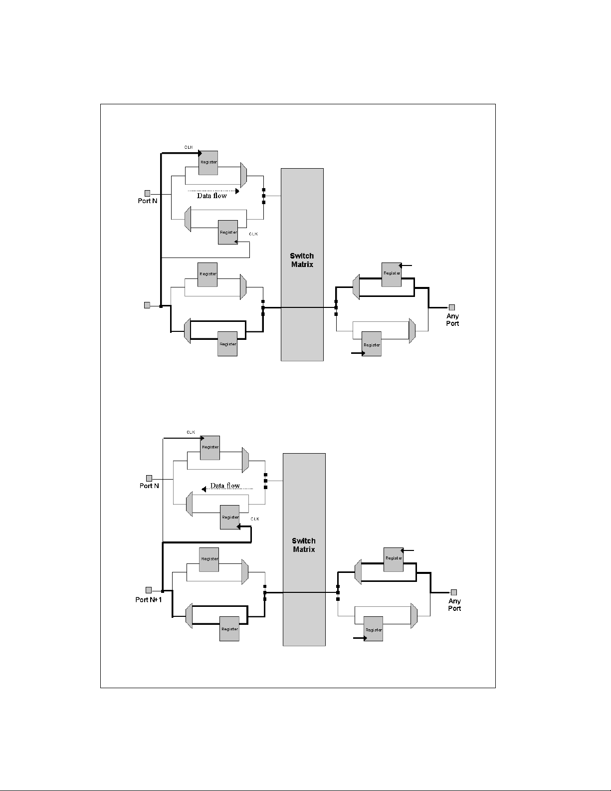
Next-Neighbor Clocking
Included among the clocking options in MSX532 is the ability to use an adjacent port as a clock source. This is
referred to as a Next-Neighbor Clock. In the MSX532, Port
0 can be clocked by Port 1, which can be clocked by Port 2,
which can be clocked by Port 3 , etc. In turn, Port 53 1 can
be clocked by Port 0. Since each I/O buffer can be programmed as an input or an outpu t (among other options)
there are four ways to utilize the next neighbor clock
option.
3 www.fairchildsemi.com
Page 4

Introduction (Continued)
MSX532
Option 1: Registered Input with Next-Neighbor Clock as Input
Option 2: Registered Output with Next-Neighbor Clock as Input
www.fairchildsemi.com 4
Page 5
Introduction (Continued)
Option 3: Registered Input with Next-Neighbor Clock as Output
MSX532
Option 4: Registered Output with Next-Neighbor Clock as Output
5 www.fairchildsemi.com
Page 6

Introduction (Continued)
MSX532
Symbol I/O Port Function Mnemonic
TAB LE 1. Summary for Programmable I/O Attributes for MSX Devices
Input The external signal is buffered from the Input Port pin to the
corresponding Switch Matrix line.
IN
Output The internal signal is buffered from the corresponding
Registered
Input
Registered
Output
Bidirectional
Transceiver
Bus
Repeater
Pin Side
Force 0
Switch Matrix line to the Output Port pin. In this mode an
optional output enable (OE
level is logic 0. The output data inversion mode is available
to invert the output signal.
The external signal at the I/O Port is registered into an edgetriggered register within the I/O Port. A clock source is
required in this mode. An input enable (IE) is available but
not required.
The internal signal on the Switch Matrix line is registered by
an edge-triggered register within the I/O Port. A clock source
is required in this mode. An output enable (OE
but not required.
The output data inversion mode is NOT available to invert
the output signal.
In this mode, the I/O buffer acts as a bidirectional transceiver
between the I/O Port pin and the corresponding Switch
Matrix line. This mode requires an input enable (IE) and output enable (OE
The output data inversion mode is available to invert the output signal.
In the Bus Repeater mode, the I/O Port behaves as a wire
(with a non-zero propagation delay). This unique feature
patented by Fairchild incorporates as self-sensing circuit to
determine signal direction and does not require a direction
control signal.
When multiple I/O Ports, configured as “Bus Repeater”, are
connected together through the Switch Matrix to form a single internal node, any (open collector or 3-STA TABLE) LOW
(logic “0”) external signal appearing a t any one of the I/O
Ports gets repeated (or broadcast) to other I/O Ports. For
more details, refer to the Technical Note: “The Bus Repeater
Mode”
In this output mode, the I/O Port pin is forced LOW (logic 0),
regardless of the signal on the corresponding switch Matrix
line. In this mode an optional output enable (OE
selected.
).
) can be selected. The default
) is available
) can be
OP
RI
RO
BT
BR
F0
Pin Side
Force 1
No Connect In this mode, the I/O Port pin is isolated from the Switch
Array Side
Force 0
www.fairchildsemi.com 6
In this output mode, the I/O Port pin is forced HIGH (logic 1),
regardless of the signal on the corresponding Switch Matrix
line. In this mode an optional output enable (OE
selected.
Matrix. This is done by 3-STA TING both the input and output
part of the I/O buffer.
In this input mode, the Switch Matrix line is forced LOW
(logic 0), regardless of the signal on the corresponding I/O
Port. In this mode an optional input enable (IE) can be
selected.
F1
) can be
NC
A0
Page 7

Introduction (Continued)
DQ
IE
AxPx
CLK
OE
DQ
IE
Ax Px
CLK
OE
D1Q
1
IE
AxPx
CLK_IN
OE
CLK_OP
Q
0D0
Array Side
Force 1
In this input mode, the Switch Matrix line is forced HIGH
(logic 1), regardless of the signal on the corresponding I/O
Port. In this mode an optional input enable (IE) can be
selected.
MSX532
A1
Bidirectional
Transceiver
with
Register
Input
Bidirectional
Transceiver
with
Register
Output
Bidirectional
Transceiver
with
Register I/O
This mode combines Registered Input and buffered Output
(OP). This mode requires a clock source (CLK), and input
enable (IE) and output enable (OE
This mode combines Registered Output (RO) and buffered
Input (IE). This mode requires a clock source (CLK), and
input enable (IE) and output enab le (OE
The output data inversion mode is NOT available to invert
the output signal.
This mode combines Registered Input (RI) and Registered
Output (RO). This mode requires a clock source (CLK), and
input enable (IE) and output enab le (OE
The output data inversion mode is NOT available to invert
the output signal.
).
).
).
BT & RI
BT & RO
BT, RI &
RO
7 www.fairchildsemi.com
Page 8
Introduction (Continued)
Control Signals
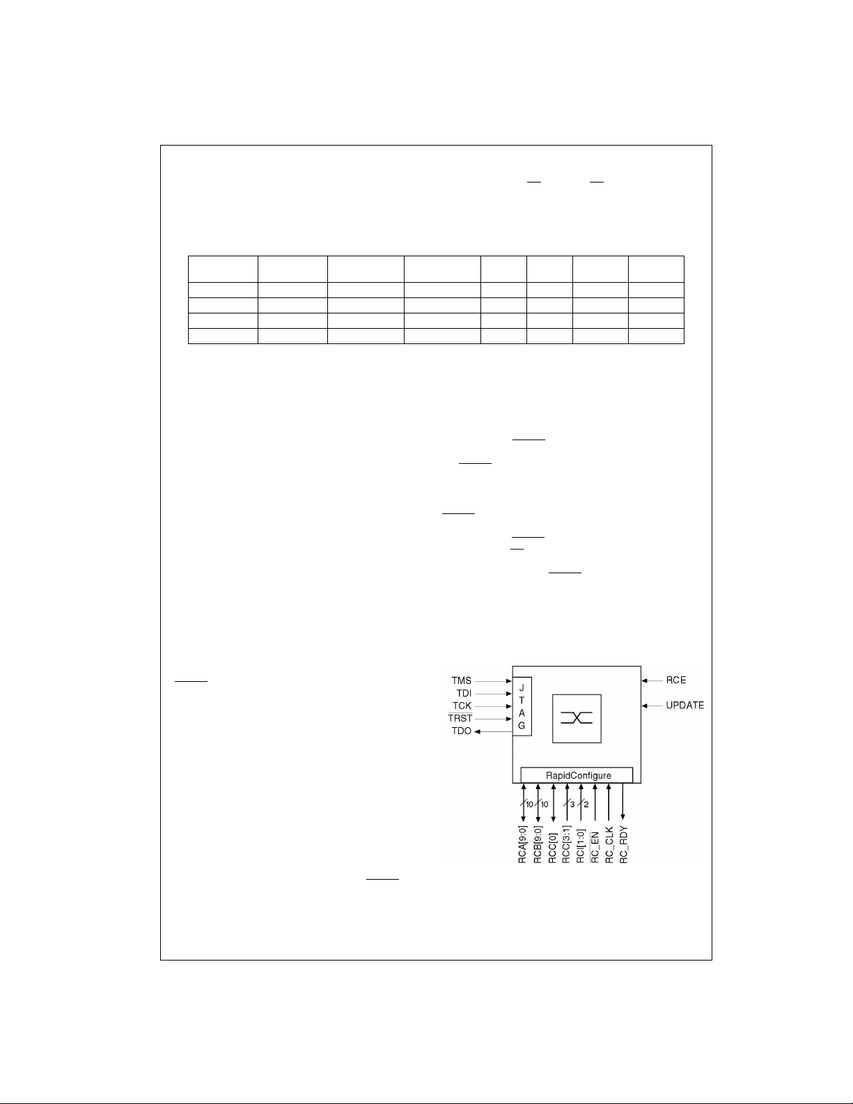
Every port on the MSX devices has two availabl e global
MSX532
clock inputs, input enable s, and output enables. Howeve r,
not all ports have a ccess to the same global control sig nals. There are four global clocks (CLK_0 throug h CLK _3 ),
TABLE 2. M SX Global Control Signals
MSX340 Port
Number
Ports 0-84 Ports 0-132 CLK_0 CLK_1 IE_0 IE_1 OE_0 OE_1
Ports 85-169 Ports 133-265 CLK_1 CLK_2 IE_1 IE_2 OE_1 OE_2
Ports 170-254 Ports 266-398 CLK_2 CLK_3 IE_2 IE_3 OE_2 OE_3
Ports 255-339 Ports 399-531 CLK_3 CLK_0 IE_3 IE_0 OE_3 OE_0
MSX532 Port
Number
Input/Output
Clock Source 1
four global input enables (IE_0 through IE_3), and four global output enables (OE
trol signal is available to half of the ports on the MSX
device. Table 2 below shows the global control sign als that
are available to each port.
Input Output
Clock Source 2
Input
Enable 1
_0 through OE_3). Each global con-
Input
Enable 2
Output
Enable 1
Output
Enable 2
RapidConfigure Interface
The MSX family of Digital Crosspoint Switches can be configured in either of two ways. Both the JTAG serial programming interfac e and the RapidConfigure (RC) par allel
interface can assign crossp oint connectio ns and configure
I/O buffers, but JTAG is a serial input and is slower. JTAG
runs reliably up to 8 MHz and requires over twenty cycles
to program a single command. The RapidConfigur e interface can run at up to 40 MHz a nd can send a new command on every clock cycle. Systems requiring frequent
reconfiguration sh ould be designed to use the RapidC onfigure interface.
RapidConfigure is a 29 signal parall el interface that effectively flattens the serial JTAG bitstream. Rather than con secutively shifting in tw enty or so bits of data to configure
an I/O buffer or make a crosspoint connection, all of these
bits are driven o n the RC lines simultaneously a nd then
latched in by the MSX device in a single cycle. Additionally,
the MSX RapidConf igure interface has b een enhanced to
enable read ing back of configuration data from the device.
RCA[9:0] = RapidConfigure Address A
RCB[9:0]
RCC[3:0]
RCI[1:0]
RC_CLK
RC_EN
RC_RDY
Signal Descriptio n
The RC interface su pports four types of operation s. Two
are write operations to the M SX (I/O b uffer configu ra tion or
crosspoint progr amming) an d two are read operatio ns (I/O
buffer and crosspoint configuration read). The RC signals
serve different purp ose s dep ending upon the t ype of o peration being performed.
Most of the signals on th e MSX device’s RC interface are
bi-directional. These signa ls r ec e iv e d ata du r i ng wri t e op erations. During read oper atio ns the se pi ns re ceive data during the first part of the cycle, an d the n drive t he inte rfa ce i n
the final part of the cycle. RCA[9:0], RCB[9:0], and RCC[0]
are bi-directional pins. RCC[3:1], RC_CLK, RC_EN
= RapidConfigure Address B
= RapidConfigure Program Variable C
= RapidConfigure Instruction Bits
= RapidConfigure Clock
= RapidConfigure Cycle Enable
= Read out I/O buffer
and connect/disconnect status
, and
RCI[1:0] are dedicated inputs. RC_RDY is a dedicated output.
The RC_CLK signal is the str obe that latches write data
into the MSX device. I t synchronize s the s ignals driven on
to the RC interface and determines the rate at which commands can be loaded into the MSX device. The MSX
device latches command data on the falling edge of
RC_CLK when RC_EN
can be repeated on consecutive clock s simply by keeping
the RC_EN
on the RCA, RCB, RCC, and RCI signals. RC Read operations require four AC clock cycles and cannot be performed
on back-to-back clocks.
RC_EN
tion. Back-to-back RC Write oper ations may be perf ormed
by keeping the RC_EN
operations RC _EN
complete. Back-to-back RC Read operatio ns can be executed simply by keeping RC_EN
The MSX device as sert s R C_RD Y w h en it has entered the
final stage of a read an d data out is ready. RC_RDY is
asserted on the falling edge of RC_CLK, and de-asserted
on the next falling edge. The MSX device will be driving
valid read data on the RC interface when RC_RDY is
asserted HIGH.
The RC interface specif ies that the RC I sign als b e used to
determine the type of operation being performed.
signal asserted and providing new commands
is an Active LOW signal that enables an RC opera-
FIGURE 4. MSX Switch Configuration Signals
is asserted. RC Write operations
signal asserted. Du ring RC Read
must remain asserted until the cycle is
asserted.
www.fairchildsemi.com 8
Page 9
Introduction (Continued)
TABLE 3. RapidConfigure Input
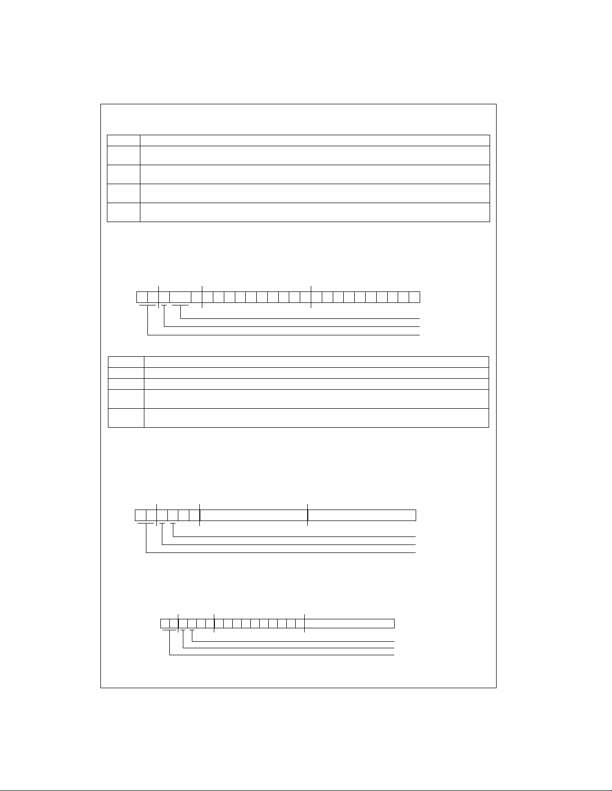
RCI [1:0] Description
Force Testing Command. Force commands can force a port to drive either a one or a zero to either the pad or
00
crosspoint array. These commands are generally only used for diagnostic testing.
I/O Buffer Programming Command. These commands are used to configure a port as an input or output,
01
registered or not, etc.
Crosspoint Array Programming Command. Crosspoint connections can be made or broken, or an individual port
10
can be reset.
Read and Reset Commands. This setting is used to read back configuration data from an I/O buffer or crosspoint
11
connection information. It can also be used to reset all of the I/O buffers and the crosspoint array.
Read and Reset Commands
When RCI[1:0] are equal to 11 a Read or Reset command is executed (see Table 4: Reset Commands).
Reset Commands
MSX532
RCI[1:0] RCC[3:0] RCB[9:0] RCA[9:0]
12301
0
789
6
345
2
901
8
567
4
123
0
1 0 0 01 0 0 0 0 0 0 0 0 0 0 0 0 0 0 0 0 0 0 0
Reset Cmd Options
Reset Command
Read/Reset Cmd
TABLE 4. Reset Commands (Continued)
RCC [2:1] Description
00 Reserved. This is not a valid command.
01 Reserved. This is not a valid command.
Crosspoint Array Reset. This command will reset the entire crosspoint array, breaking any previously existing
10
connections.
Crosspoint Array and I/O Buffer Reset. This command resets both the I/O buffers and the crosspoint array as
11
described above.
RCC[0], RCB[9:0], and RCA[9:0] have no function during a reset command and must be written as zeroes.
Crosspoint Read Commands
A crosspoint read is used to check wheth er two ports are
connected through the crosspo int array. The two ports are
addressed using RCA[9:0] and RCB[9:0]
RCI[1:0] RCC[3:0] RCB[9:0] RCA[9:0]
1 11 0 0
12301
0
0
789
6
345
Port #1 Port #2
The MSX device uses RCC[0] to show whether the two
ports are connected. It drives RCC[0] HIGH if the two ports
are connected, and pulls RCC[0] LOW if the two ports are
not connected.
901
2
8
567
4
123
0
Cross Point Read
Read Command
Read/Reset Cmd
I/O Buffer Read Commands
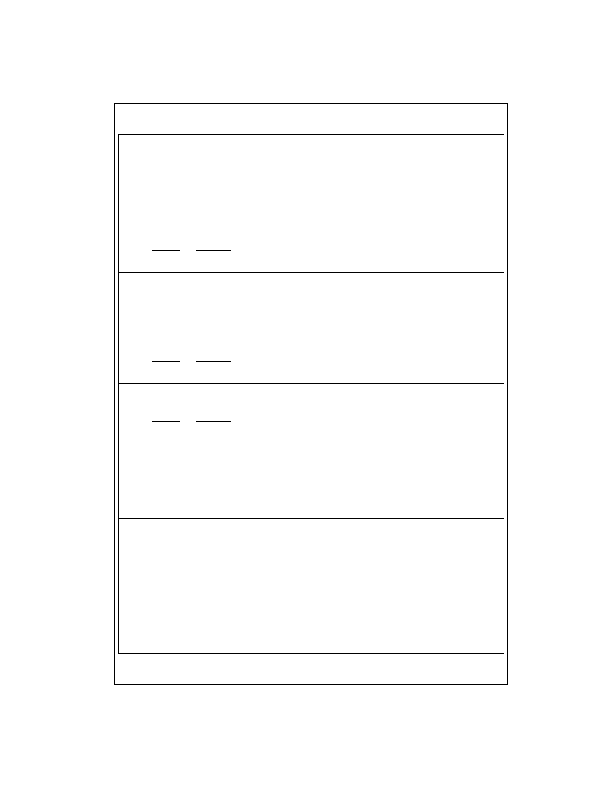
I/O Buffer reads are more comp licated (see Table 5: I/O
Buffer read Commands). The port to be read is addressed
RCI[1:0] RCC[3:0] RCB[9:0] RCA[9:0]
1 11 1 0
12301
0
0
3456789
2
using RCA[9:0]. The MSX device uses RCA[9:0] and
RCB[9:0] to return all o f the config uration data for the p articular I/O buffer.
0
901
567
8
I/O Buffer Address0 0 0 0 0 0 0 0 0 0
123
4
I/O Buffer Config Read
Read Command
Read/Reset Command
9 www.fairchildsemi.com
Page 10
Introduction (Continued)
TABLE 5. I/O Buffer Read Commands
Signal Description
MSX532
RCA[0] RCA[0] is set to one if the I/O buffer is an input. It is zero if the I/O buffer is not configured as an input. Note that an
RCA[1] RCA[1] is set to a one if the I/O buffer is an output. It is zero if the I/O buffer is not configured as an output. If
RCA[2] RCA[2] is set to a one if the I/O buffer is configured in Bus Repeater Mode. It is zero if the I/O buffer is not in Bus
RCA[3] RCA[3] is set to a one if the I/O buffer is configured as a registered input and is assigned to use its Input Clock 1.
RCA[4] RCA[4] is set to a one if the I/O buffer is configured as a registered input and is assigned to use its Input Clock 2.
RCA[5] RCA[5] is set to a one if the I/O buffer is configured as a registered input and assigned to use Next Neighbor
RCA[6] RCA[6] is set to a one if the I/O buffer is configured as a registered output and is assigned to use its Output Clock
RCA[7] RCA[7] is set to a one if the I/O buffer is configured as a registered output and is assigned to use its Output Clock
I/O buffer can be configured as an Input, Output, Input and Output (in bi-directional mode), or No Connect. All I/O
buffers default to inputs at power-on reset or following a global I/O buffer Reset command, so RCA[0] will read as
a one at reset.
RCA[0] Function
0 I/O buffer not set to input
1 I/O buffer set to input (default)
RCA[1:0] equal 00 the I/O buffer is configured as a No Connect. A No Connect means that the I/O pin of the MSX
device is not connected to the crosspoint array. RCA[1] will read as a zero at reset.
RCA[1] Function
0 I/O buffer not set to output (default)
1 I/O buffer set to output
Repeater Mode. Bus Repeater Mode will be disabled by default at reset, so RCA[2] will read as a zero.
RCA[2] Function
0 I/O buffer not set to Bus Repeater Mode (default)
1 I/O buffer set to Bus Repeater Mode
It is zero if the I/O buffer is not using Input Clock 1. Input Clock 1 for each I/O buffer will vary depending upon the
quadrant of the device in which it resides. RCA[3] will read as a zero at reset.
RCA[3] Function
0 I/O buffer not set to registered input mode (default)
1 I/O buffer set to registered input mode
It is zero if the I/O buffer is not using Input Clock 2. As with Input Clock 1, the source changes depending upon the
quadrant of the device in which the I/O buffer resides. RCA[4] will read as a zero at reset.
RCA[4] Function
0 I/O buffer not using Input Clock Source 2 in RI mode (default)
1 I/O buffer using Input Clock Source 2 in RI mode
Clocking. It is zero if Next Neighbor Clocking is disabled. Next Neighbor Clocking allows the I/O buffer to be registered using the next higher numbered Port number signal as its input clock source. Port 100 on the MSX devices
can use the signal from Port 101 for its input clock if this mode is enabled. Port 531’s Next Neighbor is Port 0. Next
Neighbor Clocking will be disabled by default at reset, so RCA[5] will read as a zero.
RCA[5] Function
0 I/O buffer not using Next Neighbor Clock in RI mode (default)
1 I/O buffer using Next Neighbor Clock in RI mode
1. It is zero if the I/O buffer is not using Output Clock 1. As with Input Clock 1 and 2, the Output Clocks will vary
depending upon the quadrant of the device in which the I/O buffer res ides. In the case of the MSX devices , the
Output Clock 1 and Input Clock 1 for each I/O buffer have the same source, and the Output Clock 2 and Input
Clock 2 do as well. RCA[6] will read as a zero at reset.
RCA[6] Function
0 I/O buffer not using Output Clock Source 1 in RO mode (default)
1 I/O buffer using Output Clock Source 1 in RO mode
2. It is zero if the I/O buffer is not using Output Clock 2. As with Output Clock 1, the source changes depending
upon the quadrant of the device in which the I/O buffer resides. RCA[7] will read as a zero at reset.
RCA[7] Function
0 I/O buffer not using Output Clock Source 2 in RO mode (default)
1 I/O buffer using Output Clock Source 2 in RO mode
I/O Buffer Read Commands (Continued)
www.fairchildsemi.com 10
Page 11

Introduction (Continued)
Signal Description
RCA[8] RCA[8] is set to a one if the I/O buffer is configured as a registered output and is assigned to use Next Neighbor
RCA[9] RCA[9] is set to a one if the I/O buffer is assigned to use Input Enable 1. It is zero if the I/O buffer is not using Input
RCB[0] RCB[0] is set to a one if the I/O buffer is assigned to use Input Enable 2. It is zero if the I/O buffer is not using Input
RCB[1] RCB[1] is set to a one if the I/O buffer is assigned to use Output Enable 1. It is zero if the I/O buffer is not using
RCB[2] RCB[2] is set to a one if the I/O buffer is assigned to use Output Enable 2. It is zero if the I/O buffer is not using
RCB[6:3] RCB[6:3] are reserved.
RCB[7] RCB[7] is set to a one if the I/O buffer is configured as an inverted output. It is zero if the I/O buffer is not config-
RCB[8] RCB[8] is set to a one if the I/O buffer is configured as a registered input and is using an inverted input clock
RCB[9] RCB[9] is set to a one if the I/O buffer is configured as a registered output and is using an inverted output clock
Clocking. It is zero if Next Neighbor Clocking is disabled. Next Neighbor Clocking allows the I/O buffer to be registered using the next higher numbered Port number signal as its output clock source. Port 100 on the MSX devices
can use the signal from Port 101 for its output clock if this mode is enabled. Port 531’s Next Neighbor is Port 0.
Next Neighbor Clocking will be disabled by default at reset, so RCA[8] will read as a zero.
RCA[8] Function
0 I/O buffer not using Next Neighbor Clock in RO mode (default)
1 I/O buffer using Next Neighbor Clock in RO mode
Enable 1. All bi-directional I/O buffers must use one of the dedicated input enable pins (IE_0, IE_1, IE_2, or IE_3)
to enable the I/O buffer to drive data into the crosspoint array. As with the dedicated clock pins, each I/O buffer can
access two input enable signals, which will vary depending upon the quadrant of this chip in which the I/O buffer
resides. RCA[9] will read as a zero at reset.
RCA[9] Function
0 I/O buffer not using Input Enable Source 1 (default)
1 I/O buffer using Input Enable Source 1
Enable 2. RCB[0] will read as a zero at reset.
RCB[0] Function
0 I/O buffer not using Input Enable Source 2 (default)
1 I/O buffer using Input Enable Source 2
Output Enable 1. All bi-directional I/O buffers must use one of the dedicated output enable pins (OE
_2, or OE_3) to enable the I/O buffer to drive the pin of the device. As with the dedicated clock pins, each I/O
OE
buffer can access two output enable signals, which will vary depending upon the quadrant of the chip in which the
I/O buffer resides. RCB[1] will read as a zero at reset.
RCB[1] Function
0 I/O buffer not using Output Enable Source 1 (default)
1 I/O buffer using Output Enable Source 1
Output Enable 2. RCB[2] will read as a zero at reset.
RCB[2] Function
0 I/O buffer not using Output Enable Source 2 (default)
1 I/O buffer using Output Enable Source 2
ured as an inverted output. The output of any I/O buffer may be inverted so long as it is not a registered output or
running in Bus Repeater Mode. RCB[7] will read as a zero at reset.
RCB[7] Function
0 I/O buffer not configured as inverted output (default)
1 I/O buffer configured as inverted output
source. It is zero if it is not using an inverted input clock. Inputs can use any of the three clock sources described
above and may invert that clock if desired. RCB[8] will read as a zero at reset.
RCB[8] Function
0 I/O buffer not using inverted clock source in RI mode (default)
1 I/O buffer using inverted clock source in RI mode
source. It is zero if it is not using an inverted output clock. Outputs can use any of the three clock sources
described above and may invert that clock if desired. RCB[9] will read as a zero at reset.
RCB[9] Function
0 I/O buffer not using inverted clock source in RO mode (default)
1 I/O buffer using inverted clock source in RO mode
_0, OE_1,
MSX532
11 www.fairchildsemi.com
Page 12
Introduction (Continued)
Crosspoint Programming
Connections between po rts through the crosspoint array
MSX532
can be quickly made or broken using the RC interface. The
two ports to be connected or disconn ected are addressed
using RCA[9:0] and RCB[9:0]. RCC[1] controls whether a
connection is made or broken. The two ports are connected when RCC[1] is set to zero, and disconnected when
RCC[1] is set to one
RCI[1:0] RCC[3:0] RCB[9:0] RCA[9:0]
12301
0
1 00 1 0
3456789
2
Port #1 Port #2
Unlike I/O buffer programming commands, which take
effect immediately upon execution of the command, crosspoint connections will only be made if the UPDATE signal
is asserted HIGH. The crosspoint programming command
loads the Loading SRAM cell in the selected crosspoint
array location with a one (in the case of a new conne ction)
or a zero (to break an exist ing c onnectio n). If th e UPDATE
signal is asserted, the Loading SRAM cells contents are
immediately tran sferred to the Active SRAM ce ll and the
connection is mad e or broken. However, if the UPDATE
signal is held LOW, the new connection will not be made.
RCI[1:0] RCC[3:0] RCB[9:0] RCA[9:0]
789012301
0 1
345
6
901
567
8
123
4
0
Connect/Disconnect
(0-Connect, 1-Disconnect)
Crosspoint Program
The UPDATE signal can be used to control when the
switch matrix connections are reconfigured.
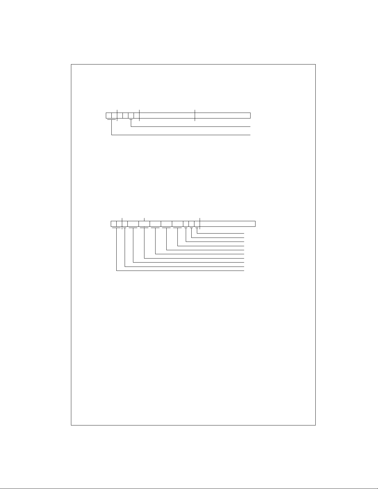
I/O Buffer Configuration Programming
Each port can be fully configured in a single RapidConfigure cycle. The figure below shows how an I/O buffer is programmed using al l of the sig nals on the RC in terface. T he
following table shows how each control bits (RCC[3:0] and
RCB[9:0]) are used. During an I/O buffer programming
command the RCA[ 9:0] sig nal s ad dre ss t he po rt to be programmed (see Table 6: I/O buffer Programming Commands)
4
123
0
Inverted Output Clock
Inverted Input Clock
Invert Output
Input Clock Source
Output Clock Source
Input Enable Select
Output Enable Select
Input/Output Select
Bus Repeater Enable
I/O Buffer Configuration
901
2
567
8
I/O Buffer Address
www.fairchildsemi.com 12
Page 13
Introduction (Continued)
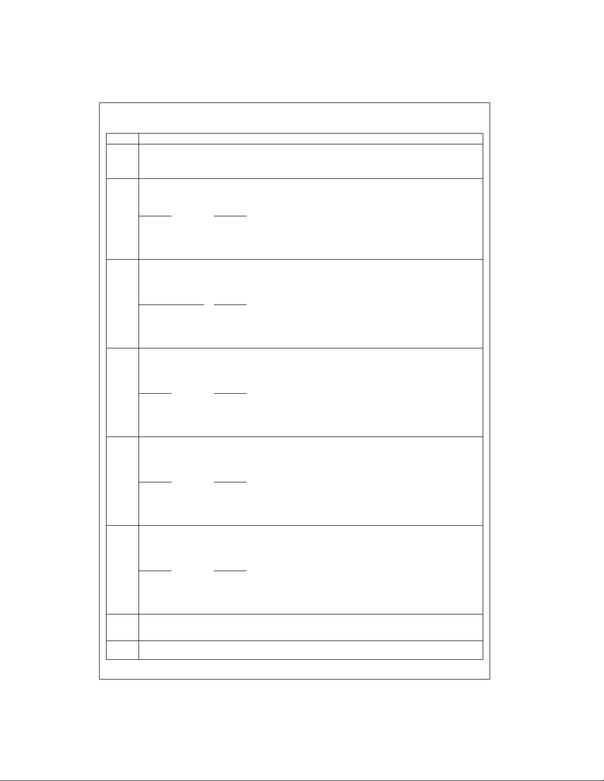
TABLE 6. I/O Buffer Programming Commands
Signal Description
RCC[3] Bus Repeater Enable. Setting this bit to a one enables the I/O buffer to operate in Bus Repeater Mode, a special
RCC[2:1] Input/Output Select. These two bits are used to configure the I/O buffer as an input, output, input/output (bi-
RCC[0]
and
RCB[9]
RCB[8:7] Input Enable Select. These bits are used to assign a port one of the two available global input enable signals. An
RCB[6:5] Output Clock Source. These bits are used to select a clock source for a registered output port. Each I/O buffer
RCB[4:3] Input Clock Source. These bits are used to select a clock source for a registered input port. Each I/O buffer can
RCB[2] Invert Output. If an output port is programmed with this bit set to a one, the output of the port will be inverted. If
RCB[1] Inverted Input Clock. When this bit is set to a one, the registered input port’s selected clock source will be
bi-directional mode. When zero the I/O buffer will not operate in Bus Repeater Mode.
When programming an I/O buffer to use Bus Repeater Mode, all of the other control bits must be set to zeroes.
Attempting to combine other I/O buffer options with Bus Repeater Mode may lead to unpredictable results.
directional mode), or no connect. When operating in bi-directional mode it is critical that the port be assigned
input and output enables so that it can be 3-STATED appropriately to avoid contention.
RCC[2:1] Function
00 No Connect
01 Input
10 Output
11 Input / Output for Bi-Directional Mode
Output Enable Select. These two bits are used to select from the two available active LOW global output
enables. The output will be allowed to drive when its assigned output enable is asserted. An output port will be 3STATED when its assigned output enable is de-asserted. When both output enables are selected, the two available active LOW output enable signals are AND’ed together to form the port’s combined output enable signal.
RCC[0], RCB[9] Function
00 No Output Enable Selected
01 Output Enable 1
10 Output Enable 2
11 Both Output Enables
input port will drive into the crosspoint array when its assigned input enable is asserted. When both input
enables are selected, the two available input enable signals are OR’ed together to form the port’s combined
input enable signal.
RCB[8:7] Function
00 No Input Enable Selected
01 Input Enable 1
10 Input Enable 2
11 Both Input Enables
can select from one of two global clock inputs, or can use Next Neighbor Clocking. Next Neighbor Clocking uses
the signal on the next higher numbered port as a clock source. If no clock source is assigned to an output port, it
will operate in flow-through mode.
RCB[6:5] Function
00 No Output Clock Source Selected
01 Output Clock Source 1
10 Output Clock Source 2
11 Next Neighbor Output Clock Source
select from one of two global clock inputs, or can use Next Neighbor Clocking. Next Neighbor Clocking uses the
signal on the next higher numbered port as a clock source. If no clock source is assigned to an input port, it will
operate in flow-through mode.
RCB[6:5] Function
00 No Input Clock Source Selected
01 Input Clock Source 1
10 Input Clock Source 2
11 Next Neighbor Input Clock Source
this bit is zero, the output will not be inverted. Outputs may not be inverted when operating in Bus Repeater
Mode or in registered output mode.
inverted. When zero the input clock source will not be inverted.
MSX532
13 www.fairchildsemi.com
Page 14
Introduction (Continued)
Signal Description
RCB[0] Inverted Output Clock. When this bit is set to a one, the registered output port’s selected clock source will be
MSX532
inverted. When zero the output clock source will not be inverted.
JTAG Interface
The dedicated JTAG TAP interface is designed in compli ance with the IEEE-1149.1. The standard interface has five
pins: Test Data Out (TDO), Test Mode Select (TMS), Test
Data In (TDI), Test Reset (TRST
which allow Boundary Scan Testing as well as device configuration and veri fication. Data on the TDI and TMS pins
are clocked into the de vice on the rising edg e of the TCK
signal, while the valid data appears on the TDO pin afte r
the falling edge of TC K. For more detailed information on
JTAG programming, refer to the MSX Family Register Programming Manual.
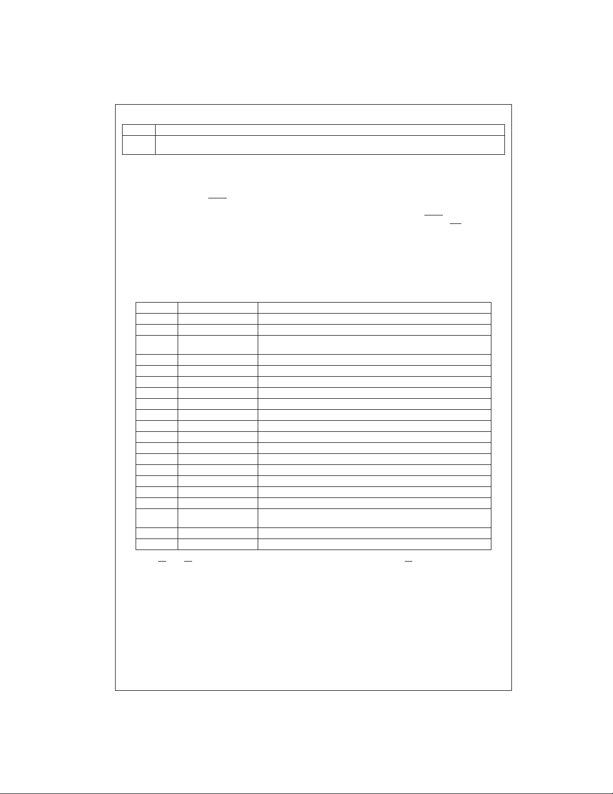
Bit Number I/O Buffer Function Description
0 Input (IN) Input Pin Data to Drive Array
1 Output (OP) Output Array Data to Pin
2 Bus Repeater (BR)
3 Reg In Clock 1 Selects Reg. In I/O Buffer, Clock 1
4 Reg In Clock 2 Selects Reg. In I/O Buffer, Clock 2
5 Reg In Clock Neighbor Selects Reg. In I/O Buffer, Neighbor
6 Reg Out Clock 1 Selects Reg. Out I/O Buffer, Clock 1
7 Reg Out Clock 1 Selects Reg. Out I/O Buffer, Clock 2
8 Reg Out Clock Neighbor Selects Reg. Out I/O Buffer, Neighbor
9 Input Enable 1 (IE_1) Select Input Enable 1 (Note 1)
10 Input Enable 2 (IE_2) Select Input Enable 2 (Note 1)
11 Output Enable 1 (OE_1) Select Output Enable 1 (Note 2)
12 Output Enable 2 (OE_2) Select Output Enable 2 (Note 2)
13 Force 1 Force I/O Buffer Output Pin to a 1
14 Force 0 Force I/O Buffer Output Pin to a 0
15 Array 1 Force I/O Buffer Array to a 1
16 Array 0 Force I/O Buffer Array to a 0
17 Invert Output
18 Invert Input Clock Invert the Clock to the Input Register
19 Invert Output Clock Invert the Clock to the Output Register
Note 1: If both IE_1 and IE_2 are selected, the two are assigned an OR function to form the IE. Either can be “1” to enable the input.
Note 2: If both OE
put.
_1 and OE_2 ar e selected, active LOW signals are assi gned an AND function t o f orm the resulting OE. Either can be “0” to enable the out-
), and Test Clock (T CK)
TABLE 7. I/O Buffer Programming Bit Functions
Low Array Signal, Drive Pin LOW
Low Pin Signal, Drive Array LOW
Output data is inverted.
This operation is invalid in Bus Repeater mode and Register Output mode
I/O Buffer Programming
The JTAG I/O Buffer Data Register where data is hel d, is
used to program the I/ O buffer. This register is used with
the JTAG interface only. The JTAG I/O buffer data register
is 20 bits wide. Power on reset, RapidConfigure reset,
Hardware reset, and JTAG reset programs all Ports as
inputs. JTAG can be reset via the TRST
five consecutive ones to the TMS pin. The HW
ware reset) pin resets and breaks all connections in the
Crosspoint Array to all no-conne cts, and the I/O buffers to
inputs.
Table 7 lists the bits and their function in JTAG mode.
These are internal bits a s shifted into the I/O buffer data
register for I/O buffer programming.
pin or by clocking
_RST (hard-
www.fairchildsemi.com 14
Page 15
Introduction (Continued)
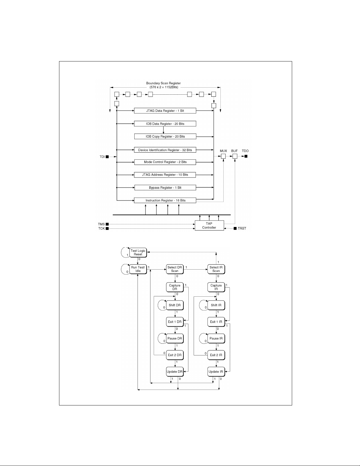
JTAG Architecture and Shift Registers
MSX532
FIGURE 5. MSX JTAG Architecture
FIGURE 6. JTAG State Machine
15 www.fairchildsemi.com
Page 16
Introduction (Continued)
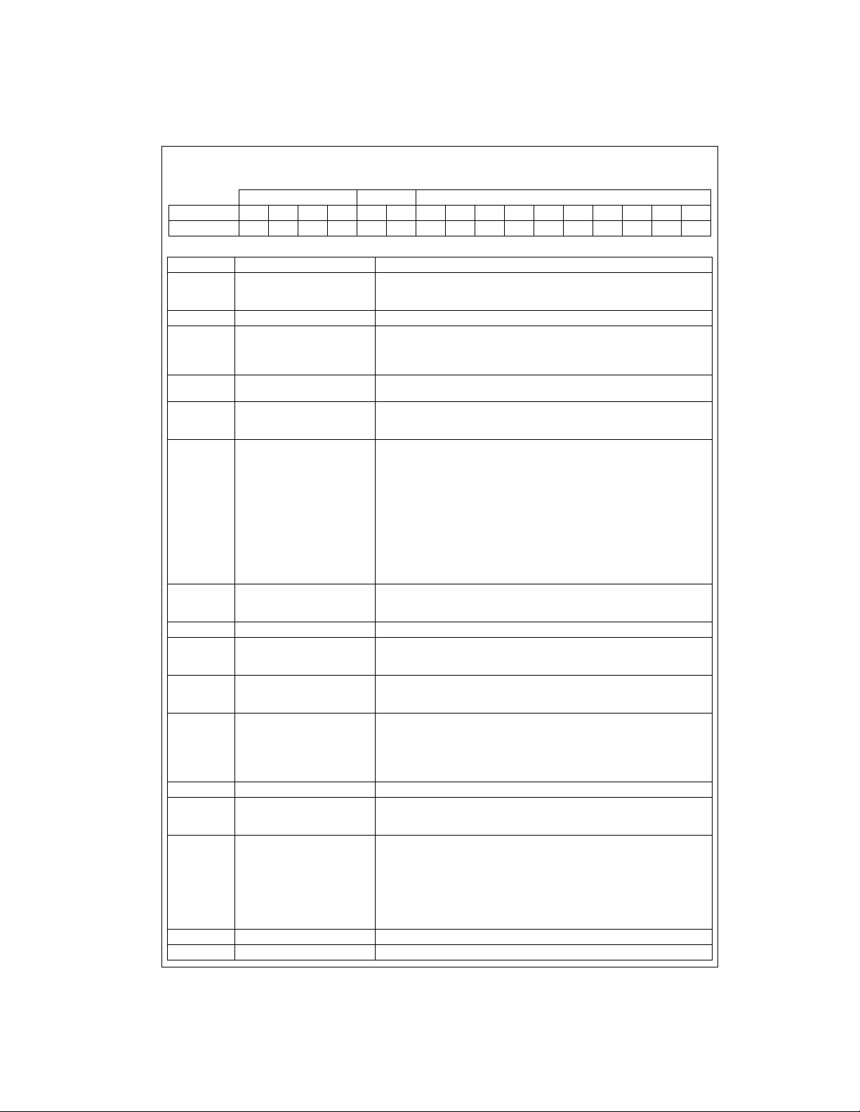
TABLE 8. JTAG Input Format
MSX532
Bit Number 15 14 13 12 11 10 9 8 7 6 5 4 3 2 1 0
Bit Name 13 12 11 10 C1 C0 A9 A8 A7 A6 A5 A4 A3 A2 A1 A0
15 14 13 12 Instruction Description
1 1 1 1 Bypass Places device in a mode to pass TDI data to TDO with one clock delay. Used
1 1 1 0 Control Bit Sets and clears the control bit A0 (LSB)
1 1 0 1 IO Buffer and
1 1 0 0 Device ID out Serialize the device ID and revision history out to TDO. ID for the MSX is
1 0 1 1 Set the JTAG Address
1 0 1 0 Access the Crosspoint Array
1 0 0 1 Disconnect a Port in the
1 0 0 0 Clear the Crosspoint Array Clear the crosspoint array at no-connect. Leave the I/O buffers unchanged.
0 1 1 1 Shift the IO Buffer Data
0 1 1 0 Shift out the I/O buffer Copy
0 1 0 1 Access an I/O buffer Read or write the I/O buffer addressed with the lower ten bits of the JTAG
0 1 0 0 Not used.
0 0 1 1 Test mode only
0 0 1 0 Crosspoint Array Write T esting,
0 0 0 0 Sample/Preload EXTEST External scan tests for interconnect testing.
0 0 0 1 Sample/Preload EXTEST External scan tests for interconnect testing.
Instruction Control Address
TABLE 9. JTAG Instructions
for programming and testing devices through serial connected JTAG controls.
Resets I/O buffers for the Ports to Input and clear all Ports to Disconnect.
Crosspoint Array Reset,
Device ID out
Register
and Update Array
Crosspoint Array
Register
Register
for programming device with
RapidConfigure through JTAG
Write one location per ShiftDR
The device ID is serialized out to TDO. The Instruction serialized out is the
RESET Instruction during the Instruction phase. Update is forced to the cros-
spoint array
0x0000A89F.
Set the 10-bit JTAG Address Register with the lower ten bits of the JTAG
Instruction Register. The lower ten bits of the JTAG Address Register
become the ’B’ Address for Crosspoint Access.
Read or Write the crosspoint addressed by the lower ten bits of the JTAG
Instruction (A Address) and the JTAG Address Register or Address Counter
(B Address). Read data is shifted out on TDO.
C1 C0 = 0 0 Read Switch with A and B Address.
Increment ’B’ address with each ShiftDR.
C1 C0 = 0 1 Connect switch at location Addressed with A and B.
Increment ’B’ address with each ShiftDR. Activate with UpdateDR.
C1 C0 = 1 0 Disconnect switch at location Addressed with A and B.
Increment ’B’ address with each ShiftDR. Activate with UpdateDR.
C1 C0 = 1 1 Force update of Switch Array Shadow regist er.
Activate with UpdateDR.
Disconnect all Ports from the Port Addressed by the lower ten bits of the
JTAG Instruction. The addressed port is reset to disconnect. The pro-
grammed state of the I/O buffer is not changed.
Shift twenty bits of data into and out of the I/O buffer Data register. The data
is used to program the I/O buffers. Parallel shift twenty bits into I/O buffer
Copy Register.
Shifts twenty bits of data out of the I/O buffer Copy Register. Data is either
the I/O buffer Data register shifted in by instruction 0111 or the last JTAG I/O
buffer Read Data.
Instruction. Read data is placed in the twenty-bit I/O buffer Copy Register.
Write Data for the I/O buffer is from the I/O buffer Data Register.
C1 C0 = 0 0 Read an I/O buffer date into the Copy Register.
C1 C0 = 0 1 Write an I/O buffer with data in I/O buffer Data Register.
Fairchild only - internal test mode to test RapidConfigure through JTAG.
Instruction Address = Lower Limit = A, Address Register = Upper Limit = B.
C1 = 1, C0 = 1 Connect all ports in address range
C1 = 1, C0 = 0 Connect Pattern=A[1] XOR B[1]
C1 = 0, C0 = 0 Connect Pattern=A[4]
C1 = 0, C0 = 1 Connect Pattern = NOT (A[1] XOR B[1]). Compliment
address limits, Address is complimented to test A-High Port to B-Low Port
connections. Other three patterns test opposite. The number of cycles =
(Sum of (X = 1), where X = Low Limit to X = High Limit) - 1
www.fairchildsemi.com 16
Page 17
Introduction (Continued)
Device Reset Options
At power-on, all MSX532 I/O buffers are set as flowthrough inputs (IN ) with input enable ON, an d the switch
matrix set to all No Connects (NC).
The RapidConfigure reset, hardware reset, and JTAG reset
functions will program the I/O buffers to flo w-through input
(IN) mode with in put e nable ON, and e ach L oading SRA M
cell in the Switch Matrix is set to No Connect. An UPDATE
Device Reset Options
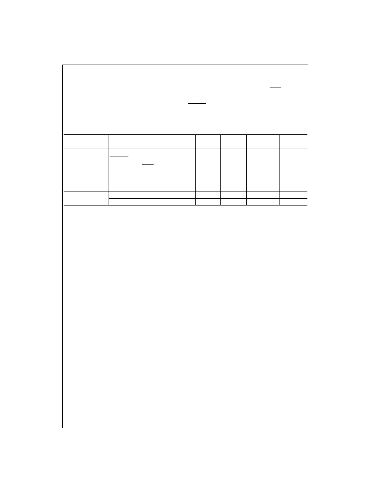
Programming Reset I/O Switch RCE Mode JTAG
Interface Method Port Matrix Control TAP
Hardware Reset Power-on Reset IN NC 1 (RC Enabled) TLR (Note 3)
HW_RST
(Low Pulse) IN NC (Note 4) 1 (RC Enabled) TLR
JTAG Reset 1. Low Pulse on TRST
2. TMS High for 5 SCLK Cycles Unchanged Unchanged Unchanged TLR
3. Device Reset (Instruction 1101) IN NC (Note 3) 1 (RC Enabled) TLR
4. Reset Crosspoint Array (Instruction 1101) Unchanged NC (Note 3) Unchanged Unchanged
RapidConfigure Reset 1. Device Reset (Instruction 1101) IN NC (Note 3) 1 (RC Enabled) Unchanged
Note 3: NC = No Connect. Each Loading SRAM cell in the Switch Matrix is updated to No Connect. An UPDATE signal is required to complete the operation
and set the Active SRAM cells to No Connect.
Note 4: TLR = Test Logic Reset State.
2. Reset Crosspoint Array (Instruction 0010) Unchanged NC (Note 3) Unchanged Unchanged
signal is required to complete the operation and set the
Active SRAM cells to No Connect.
The JTAG interface can be reset via the TRST
clocking five consecutive one to the TMS pin. The hardware reset pin can be done accomplished through the
HW_RST
pin (Active LOW). RC reset can be accomplished
by applying the RC Instruction 1101 to the RCI[3:0] pins.
Unchanged Unchanged Unchanged TLR
pin or by
MSX532
17 www.fairchildsemi.com
Page 18
Pin Description
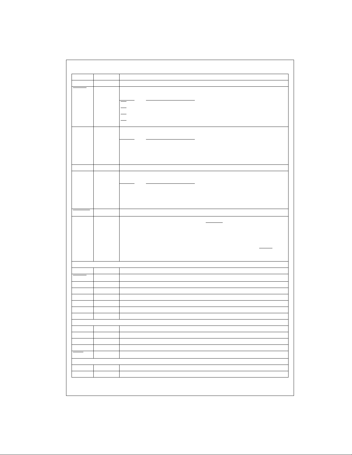
Pin Name Type Description
P[531:000] Bi-directional Input/Output Signals.
MSX532
OE[3:0]
IE[3:0] Input Global Input Enables. Each input enable can control two of the four I/O banks.
UPDATE Input Global Update
CLK[3:0] Input Global Clocks. Each clock can control two of the four I/O banks.
HW_RST
RCE Input RapidConfigure Mode Select
Input Global Output Enables. Each output enable can control two of the four I/O banks.
Signal MSX532 Connected I/O’s
OE
_0 P399-P531, P000-P132
OE
_1 P000-P132, P133-P265
OE
_2 P133-P265, P266-P398
_3 P266-P398, P399-P531
OE
Signal MSX532 Connected I/O’s
IE_0 P399-P531, P000-P132
IE_1 P000-P132, P133-P265
IE_2 P133-P265, P266-P398
IE_3 P266-P398, P399-P531
Signal MSX532 Connected I/O’s
CLK_0 P399-P531, P000-P132
CLK_1 P000-P132, P133-P265
CLK_2 P133-P265, P266-P398
CLK_3 P266-P398, P399-P531
Input Hardware Reset.
Programing mode is determined at power up or HW_RST
0 = JTAG Mode (RapidConfigure Disabled)
1 = RapidConfigure Mode (JTAG, I/O buffer, Crosspoint Programming Disabled)
Note: Device can be reconfigured from JTAG to RC or from RC to JTAG in the JTAG mode without HW_RST or power
up. In RapidConfigure mode the progra m m ing of the I/O buffers and c ros s point array through J TAG is disab led, but the
JTAG port can still be used for boundary scan testing.
RC Pins
RC_CLK Input RapidConfigure Clock.
RC_EN
RCA[9:0] Bi-directional RapidConfigure Address A.
RCB[9:0] Bi-directional RapidConfigure Address B.
RCC[0] Bi-directional RapidConfigure Program Variable C.
RCC[3:1] Input RapidConfigure Program Variable C.
RCI[1:0] Input RapidConfigure Instruction Bits.
RC_RDY Output Read Out I/O Buffer and Connect/Disconnect Status.
TCK Input JTAG Test Clock.
TDI Input JTAG Test Data In.
TDI Output JTAG Test Data Out.
TMS Input JTAG Test Mode Select.
TRST
V
DD
V
SS
www.fairchildsemi.com 18
Input RapidConfigure Cycle Enable.
JTAG Pins
Input JTAG Test and JTAG Scan Reset.
Power and Ground Pins
Power +3.3V power for the chip.
Ground Ground for the chip. Tie these pins to system ground.
Page 19
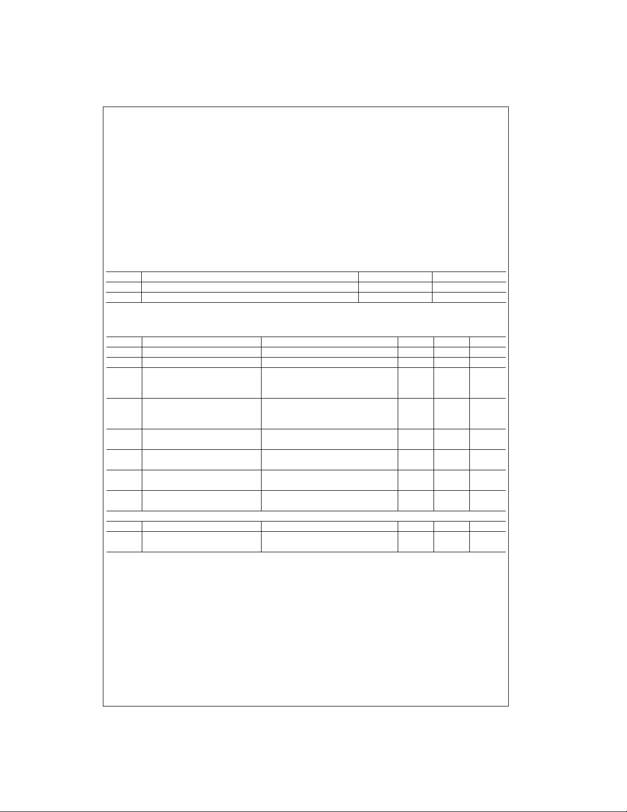
Absolute Maximum Ratings(Note 5) Recommended Operating
Supply Voltage V
DD
Supply Voltage (Inputs) V
IN
-0.3V to +3.6 V
(Note 6)(Note 7) -0.3V to +5.5V
Junction Temperature T
Storage Temperature T
J
STG
Maximum Power Dissi pat ion P
MAX
+150°C
-65°C to +150°C
Electrostatic Discharge ESD (Note 8) 1500V
Conditions
Supply Voltage V
Operating Temperature T
Note 5: The Absolute Maxi mum Ratings are thos e values beyond which
the safety of the d evice cannot b e guaranteed . The device sh ould not be
operated at these limit s. The parametric values defi ned in the Electrical
Characteristics tables are not guaranteed at the Absolute Maximum Rat-
10.5W
ings. The “Recommended Operating Conditions” table will define the conditions for actual device operation .
Note 6: A maximum undersho ot of 2 V for a max imum durati on of 20 n s is
acceptable. Overs hoot to 5.5V is acceptable.
Note 7: All inputs are 5V to lerant with the V
Note 8: Measured using Human Body Model.
DD
A
pin at 3.3V.
DD
+3.0V to +3.6V
Pin Capacitance (Note 9)
Symbol Parameter Limits Units
C
CLK
C
PORT
Note 9: Capacitance measured at 25°C. Sample tested only.
Input Capacitance 10.0 pF
I/O Signal Port Capacitance 8.0 pF
MSX532
0°C to +70°C
DC Electrical Characteristics (T
Symbol Parameter Conditions Min Max Units
V
IH
V
IL
V
OH
V
OL
I
LIH
I
LOZ
I
OSH
I
OSL
I
DDQ
Q
(Note 10) One Input Cycling @ 50% Duty Cycle
Note 10: See Power C onsumption sectio n fo r dy namic power consumption calculation.
HIGH Level Input Ports are 5V Tolerant 2.1 5.25 V
LOW Level Input Ports are 5V Tolerant -0.3 0.8 V
HIGH Level Output VDD = Min
LOW Level Output VDD = Min
, I
Input Leakage VDD = Max +5.0
LIL
for Non-programmable I/O pins 0.0 < I
3-STATE Leakage Output OFF State VDD = Max +5.0
Short Circuit Current, VDD = Max
Out = HIGH V0 = GND
Short Circuit Current, VDD = Max
Out = LOW V
Quiescent Supply Current VDD = Max 96.0 mA
Dynamic Supply Current VDD = Max. No Load, 0.375 mA/MHz
DDD
= 0°C to 70°C, VDD = 3.3V ±10%)
A
IOH = -4 mA
= 3.00
DD
IOL = 8 mA
< V
n
DD
0.0 < I
< V
n
DD
= V
0
DD
Supply Current
2.4 V
+ 0.3 VVDD = 3.00
DD
0.4 VV
-600
-100
-80.0 mA
80.0 mA
µA
µA
19 www.fairchildsemi.com
Page 20
AC Electrical Characteristics (T
= 0°C to 70°C, VDD = 3.3V ±10%)
A
Symbol Parameter Min Max Units
R
DATA
MSX532
f
RIO
t
W_RIO
t
S_RI
t
S_RO
t
H_RI
t
H_RO
t
CO_RO
t
CO_RI
t
PHL
t
MC
t
W+
t
W-
t
SK
t
PZH_IT
t
PZL_IT
t
PZH_OT
t
PZL_OT
t
PZH_OT
t
PZL_OT
t
RC
t
W+_RC
t
W-_RC
t
S_RC
t
H_RC
t
P_RC
t
P_RD
t
P_UD
f
JTAG
t
W_JTAG
t
S_JTAG
t
H_JTAG
t
P_JTAG
Refer to Figure 7 for AC test conditions.
NRZ Data Rate 150 Mb/s
Registered Input/Output Clock Frequency 75.0 MHz
Registered Clock Pulse Width, HIGH or LOW 3.0 ns
Registered Input Setup Time to Clock 5.0 ns
Registered Output Setup Time to Clock 9.5 ns
Registered Input Clock to Hold Data 0.0 ns
Registered Output Clock to Hold Data 0.0 ns
Registered Output Clock to Data Out Valid 11.0 ns
Registered Input Clock to Data Out Valid 24.0 ns
, t
One Way Signal Propagation Delay, Fanout = 1 20.0 ns
PLH
Delta Additional Delay Per Output Multicast (MC) Mode 2.0 ns
Input Flow-through Positive Pulse Width 6.0
Input Flow-through Negative Pulse Width 6.0
Skew 4.0 ns
, Input Enable to Valid Data 20.0 ns
, Output Enable to Valid Data 7.5 ns
, Output Enable to High Z State 7.5 ns
RapidConfigure Clock Period 20.0 ns
RapidConfigure Clock Pulse Width 8.0 ns
RapidConfigure Address Setup to RC Clock 1.0 ns
RapidConfigure Address Hold Time to RC Clock 4.0 ns
Read Back Access Time 9.0 ns
RC_RDY to Readback Data 4.0 ns
Update of Crosspoint to Data Out 10.0 ns
JTAG Clock Frequency (TCK) 8.0 MHz
JTAG Clock Pulse Width (TCK) at 8 MHz Cycle 48.0 72.0 ns
JTAG Setup Time 4.0 ns
JTAG Hold Time 0.0 ns
JTAG Clock to Output Data Valid (TDO) 10.0 ns
www.fairchildsemi.com 20
Page 21
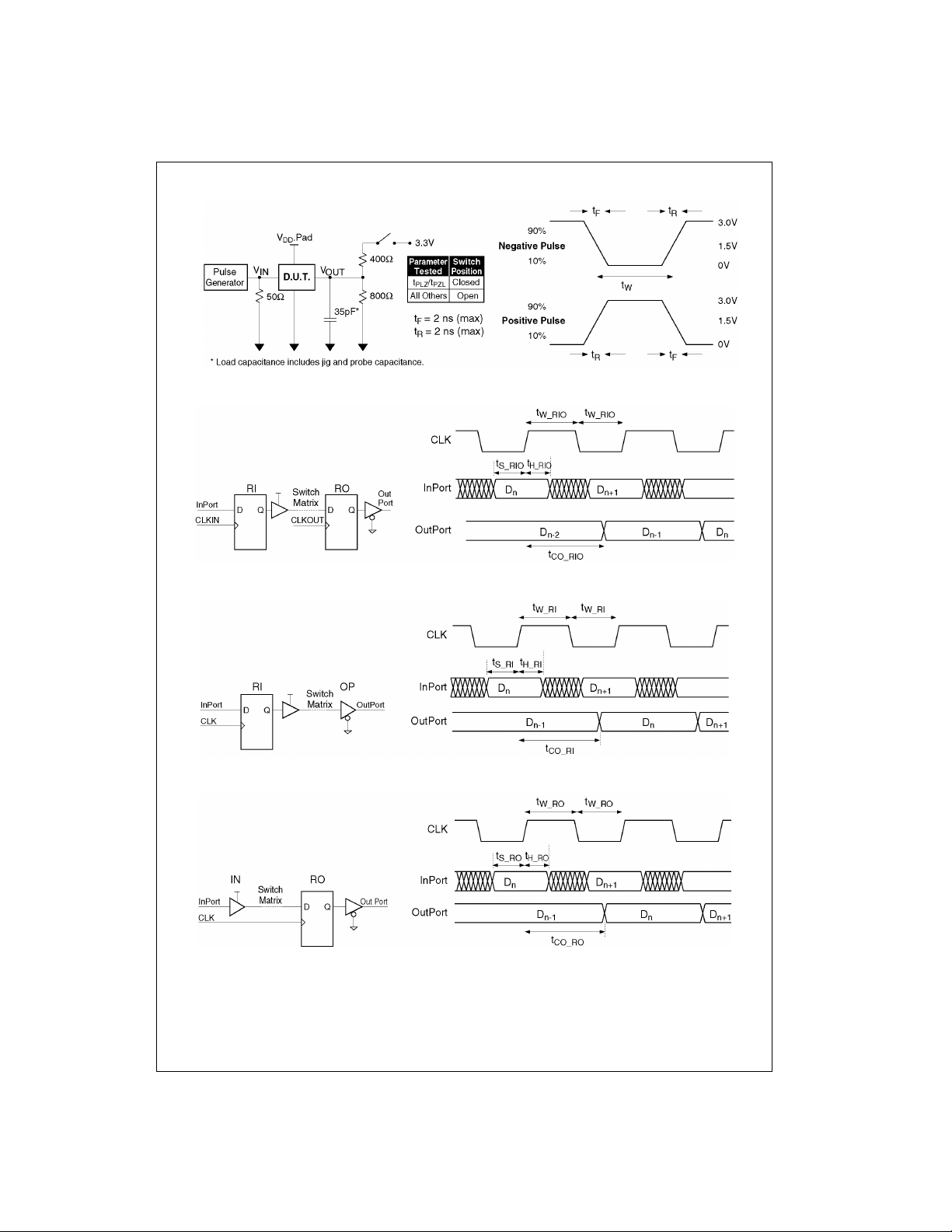
Test Circuit and Timing Diagrams
FIGURE 7. Test Circuit and Waveform Definition
FIGURE 8. Registered Input and Registered Output Mode Timing (ICLK and OCLK Synchronized)
MSX532
FIGURE 9. Reg istered Input Timing Mode
FIGURE 10. Registered Output Timing Mode
21 www.fairchildsemi.com
Page 22
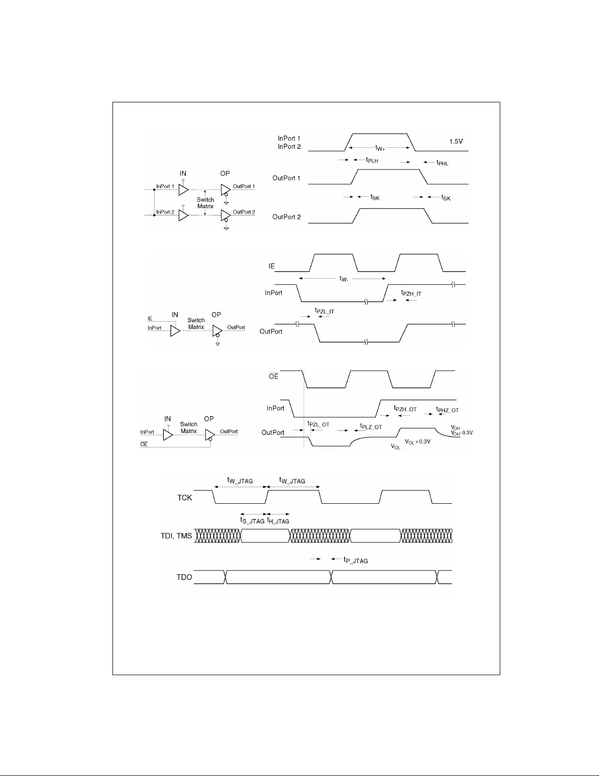
Test Circuit and Timing Diagrams (Continued)
MSX532
FIGURE 11. I/O Port Timing (Flow-through Mode)
FIGURE 12. Input Enable Timing (Flow-through Mode)
FIGURE 13. Output Enable Timing
FIGURE 14. JTAG Timing
www.fairchildsemi.com 22
Page 23
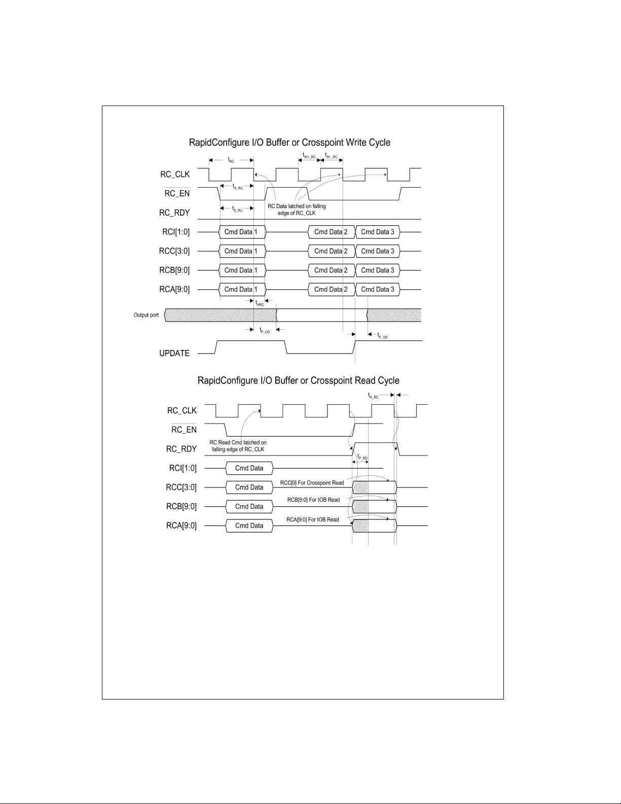
Test Circuit and Timing Diagrams (Continued)
MSX532
FIGURE 15. RapidConfigure I/O Buffer or Crosspoint Read and Write Cycles
23 www.fairchildsemi.com
Page 24
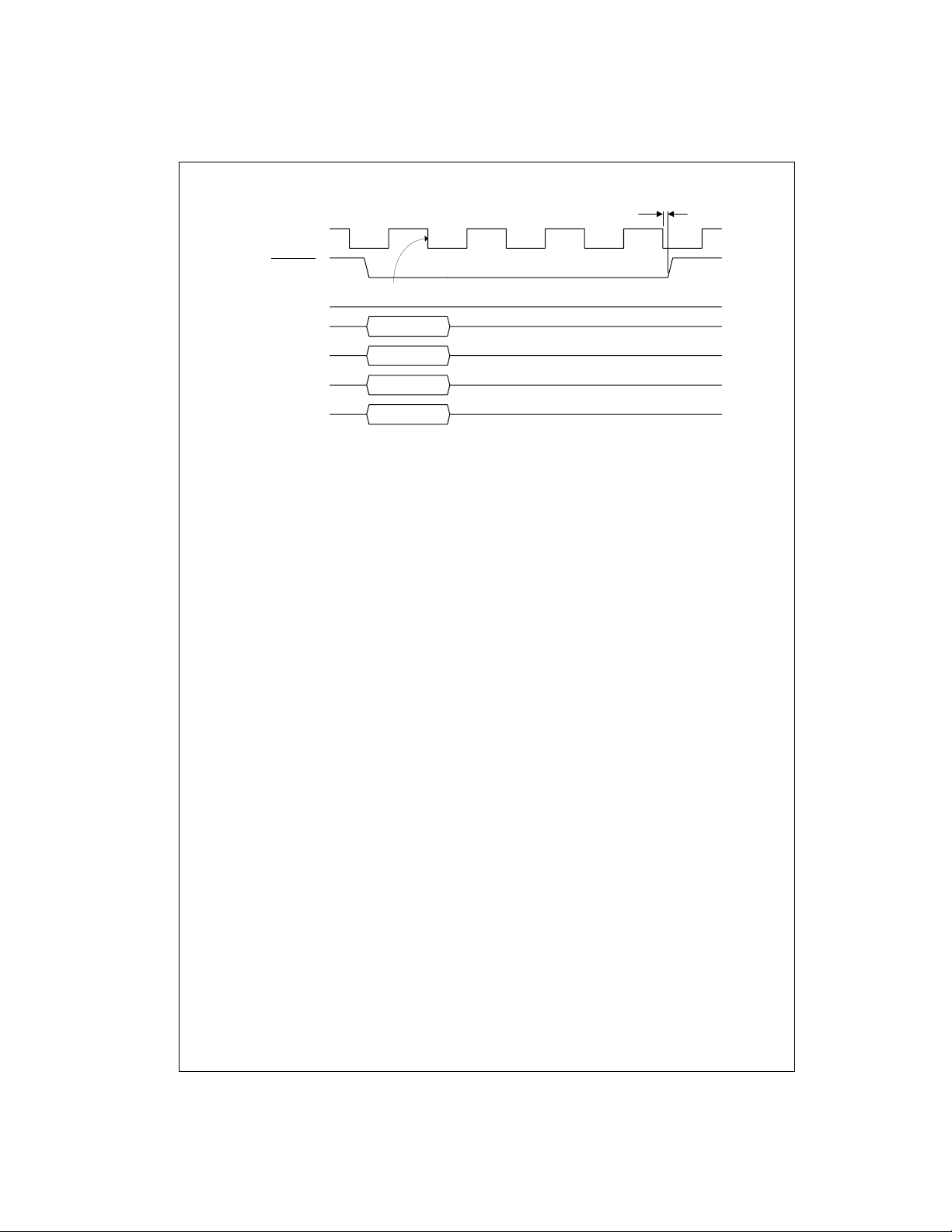
Test Circuit and Timing Diagrams (Continued)
MSX532
RC_CLK
RC_EN
RC Read Cmd latched on
RC_RDY
falling edge of RC_CLK
t
H_RC
RCI[1:0]
RCC[3:0]
RCB[9:0]
RCA[9:0]
Reset Cmd Data
Reset Cmd Data
Cmd Data
Cmd Data
FIGURE 16. RapidConfigure Reset Command Cycle
www.fairchildsemi.com 24
Page 25
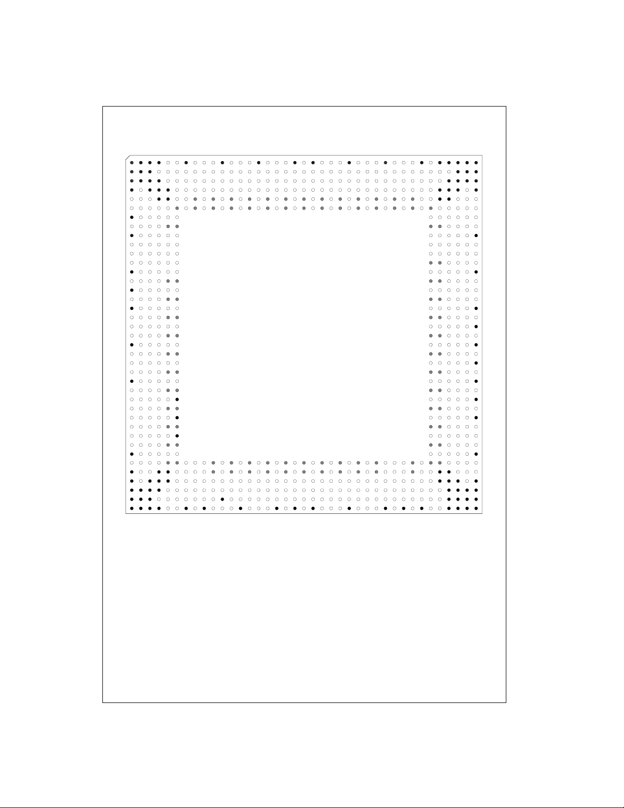
Package and Pinout
MSX532 [792 TBGA Package] Pinout
Vss
P016
P02
2
P017
P02
0
P015
P02
1
P01
P01
4
8
Vdd
P019
Vdd
P391
P389
Vdd
P388
P395
P393
P392 P382
P390 P383
P03
Vss Vss Vss
P050
3
P03
P02
P03
7
6
P040 Vss Vss
1
P03
P02
P03
4
4
P041 Vss Vss
0
P03
P02
P02
5
5
P039
8
P03
P02
P02
2
3
P038
9
Vdd
Vdd
P027
P036
Vdd
Vdd
Vss Vss
P065
P055
P044
P051
P061 P064
P060
P054
P045
P048
P058 P066
P063
P052
P042
P059
P049
P062
P053
P043
P047
Vdd
P046
Vdd
P069
P056
Vdd
Vdd
P057
Vdd
Vdd
Vss
P075
P074
P077
P072
P076P067
P073
P079
Vdd
P078
Vdd
P092
P089
P095
P085
P091
P094
P084
P083
P090
P096
P087
P082
P093
P097
P086
Vdd
Vdd
P099
P088
Vdd
Vdd
P112
Vss
P109P098
P119
P102
P113
P100
P108
P118
P104
P115
P101
P111
P120
P105
P114
P103
P110
P121
P107
P117
Vdd
Vdd
Vdd
P106
P116
Vdd
Vdd
Vdd
MSX532
in 792 TBGA
Top View
P290
P341
P373
P380
Vdd
Vdd
P370
P381
Vdd
Vdd
P371
P378
P376
P385
P369P386
P379
P374
P384
P377
P368Vss
P375P401
Vss
P366P387
P372P400
P353
P363
Vdd
Vdd
P367
P364
P365
P362
Vdd
Vdd
P340
P352
P361
Vdd
Vdd
P350
P360
P358
P359
Vss
P343
P346
P357
P351
P342
P347
P356
P348
P344
P354
P349
Vss
Vss
P355
P345
P321
P331
Vdd
Vdd
P323
P330
Vdd
Vdd
P322
P332
P327
P336
P325
P333
P337
P326
P324
P335
P339
P328
Vss
P334
P338
P329
P303
P310
Vdd
P312
Vdd
Vdd
P313
P316
P306
P315
P309
P319
P314
P318
P308
P317
P320
P311
27 28 29 30 31 32 33 34 35 36
Vdd
P296Vdd
P293
P302
P297
Vdd
P292
P304
P299
P286
P295
P305
P298
P289
P307
P294
P301
P288
Vss
Vss
P300
P291
Vss
A
Vss
B
Vss
C
Vss Vss
D
RCA6
E
RCB1
F
Vss
G
RCB7
H
Vss
J
RCE
K
P526
L
P521
M
Vss
N
P512
P
Vss
R
P502
T
Vss
U
V
P488
W
P485
Y
Vss
AA
P479
AB
P475
AC
P468
AD
Vss
AE
P458
AF
AG
P451
AH
P443
AJ
P441
AK
P433
AL
P432
AM
Vss
AN
P424
AP
Vss
AR
Vss
AT
Vss
AU
Vss Vss
AV
Vss Vss
AW
1234567891011121314151617181920212223242526
#
Vss
Vss
HW_RS
Vss
T#
CLK_
Vss
0
IE_0
Vss
Vss
Vss
Vss
RCA1
Vss
Vss
RCA0
Vss
RCA3
RCA2
RCA5
RCA4
RCA8
RCA9
RCB2
RCB0
RCB3
Vdd
RCB5
RCB4
RCB6
RCB9
RCC1
RCC0
RCC2
RCI0
RC_CLK
RC_E
RCI1
N#
P530
P529
P531
P528
P525
P522
P524
P523
P518
P516
P519
P517
Vdd
P515
P514
P513
P511
P509
P508
P506
Vdd
P505
P507
P504
P500
P498
P501
P499
VddP495
P496
P497
P494
P492
P491
P490
P489
Vdd
P486
P487
P484
P481
P478
P483
P482
Vdd
P477
P474
P476
P471
P472
P470
P473
Vdd
P467
P465
P466
P462
P460
P463
P464
P457
Vdd
P456
P459
P455
P453P450
P452
P454
P448
Vdd
P446
P449
P444
P442
P445
P447
P438
Vdd
P439
P440
P437
P435
P434
P436
P431
Vdd
P428
P430
P426
P425
P427
P429 P423
Vdd
P420
P419
P422
Vss
P418
Vss
P421
Vss
Vss
OE_3
Vss
#
P417
Vss
Vss
Vss
P415
Vss
CLK_
3
Vss
P410
Vss
TRST
Vss
P01
Vss
2
P00
P00
P00
P01
7
0
2
3
P00
P00
P00
P01
6
1
3
0
P00
TMS
4
TCK
P011
P00
RC_R
5
DY
TDO
P008
OE_0
Vdd
P00
#
TDI
9
Vdd
Vdd
RCA7
Vdd
RCB8
RCC3
UPDAT
E
P527
P520
Vdd
P510
Vdd
P503
Vdd
P493
Vdd
P480
Vdd
P469
Vdd
P461
Vdd
Vss
Vdd
Vss
Vdd
Vss
Vdd
P398
P413
P404
Vdd Vdd
P411
P399
P405
IE_3
P409
P396
P402
P416
P408
P397
P403
P414
P406
P394
P412
Vss
Vss
P407
MSX532
P125P080P071
P126P081P070
P130
P132
P135
Vdd
P138
P150
P157
P163
Vdd
P172
P180
Vdd
P190
P200
P213
P223
P240
P249
P258
P271
P279
P281
P280
OE_2#
P284
37 38 39123456789101112131415161718192021222324252627282930313233343536
Vss
Vss
P128
P131
P133
Vss
Vss
Vss
Vss
Vss
CLK_1
P137
P136
P141
P140
Vdd
Vdd
P147
P152
P153
P156
P159
P162
P165
Vdd
P168
P173
P175
Vdd
Vdd
P177
P183
P182
Vdd
P186
P192
P193
Vdd
Vdd
P197
P201
P203
Vdd
Vdd
P206
P212
P210
Vdd
Vdd
P217
P220
P221
Vdd
Vdd
P227
P231
P228
Vdd
Vdd
P234
P238
P239
Vdd
Vdd
P245
P248
P246
Vdd
Vdd
P253
P259
P257
Vdd
Vdd
P262
P268
P269
Vdd
Vdd
P274
Vss
Vss
Vss
Vss
P276
Vss
P278
Vss
CLK_2
Vss
Vss
Vss
Vss
Vss
IE_1
P134
OE_1#
P139
P143
P144
P149
P148
P155
P154
P158
P160
P164
P167
P169
P171
P174
P176
P178
P184
P185
P189
P188
P195
P194
P196
P199
P202
P205
P207
P204
P211
P209
P216
P214
P218
P219
P225
P224
P229
P226P230
P235
P233
P236
P237
P242
P243
P247
P244
P252
P250
P256
P254
P263
P260
P267
P264
P272
P270
P277
P273
Vss
P275
Vss
Vss
VssVss
VssVss
37 38 39
A
B
C
Vss
D
P142
E
P145P068
F
P146
G
P151
H
Vss
J
P161
K
P166
L
P170
M
Vss
N
P181P179
P
P187
R
P191
T
Vss
U
P198
V
Vss
W
P208
Y
Vss
AA
P215
AB
Vss
AC
P222
AD
Vss
AE
P232
AF
Vss
AG
P241
AH
Vss
AJ
P251
AK
P255
AL
P261
AM
Vss
AN
P265
AP
P266
AR
Vss
AT
Vss
AU
Vss
AV
Vss
AW
Vss
P123
P122
P124
P127
P129
IE_2
P283
P282
P285
P287
Vss
25 www.fairchildsemi.com
Page 26
Package and Pinout (Continued)
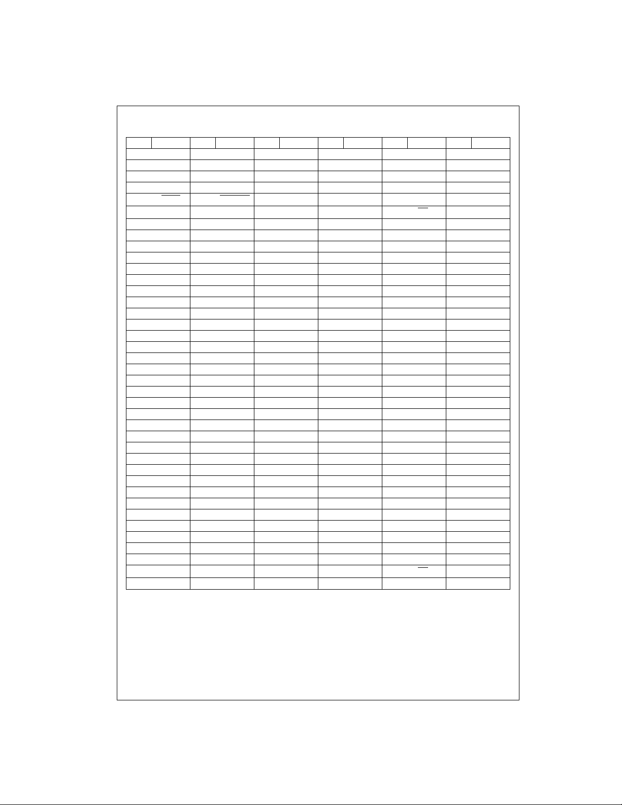
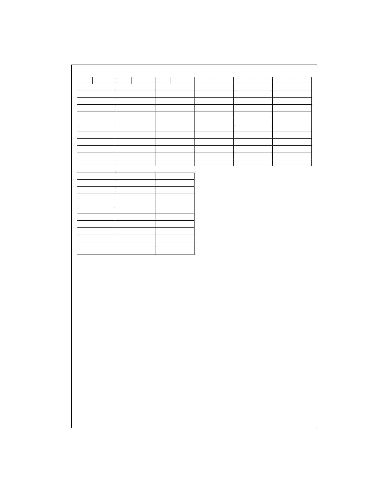
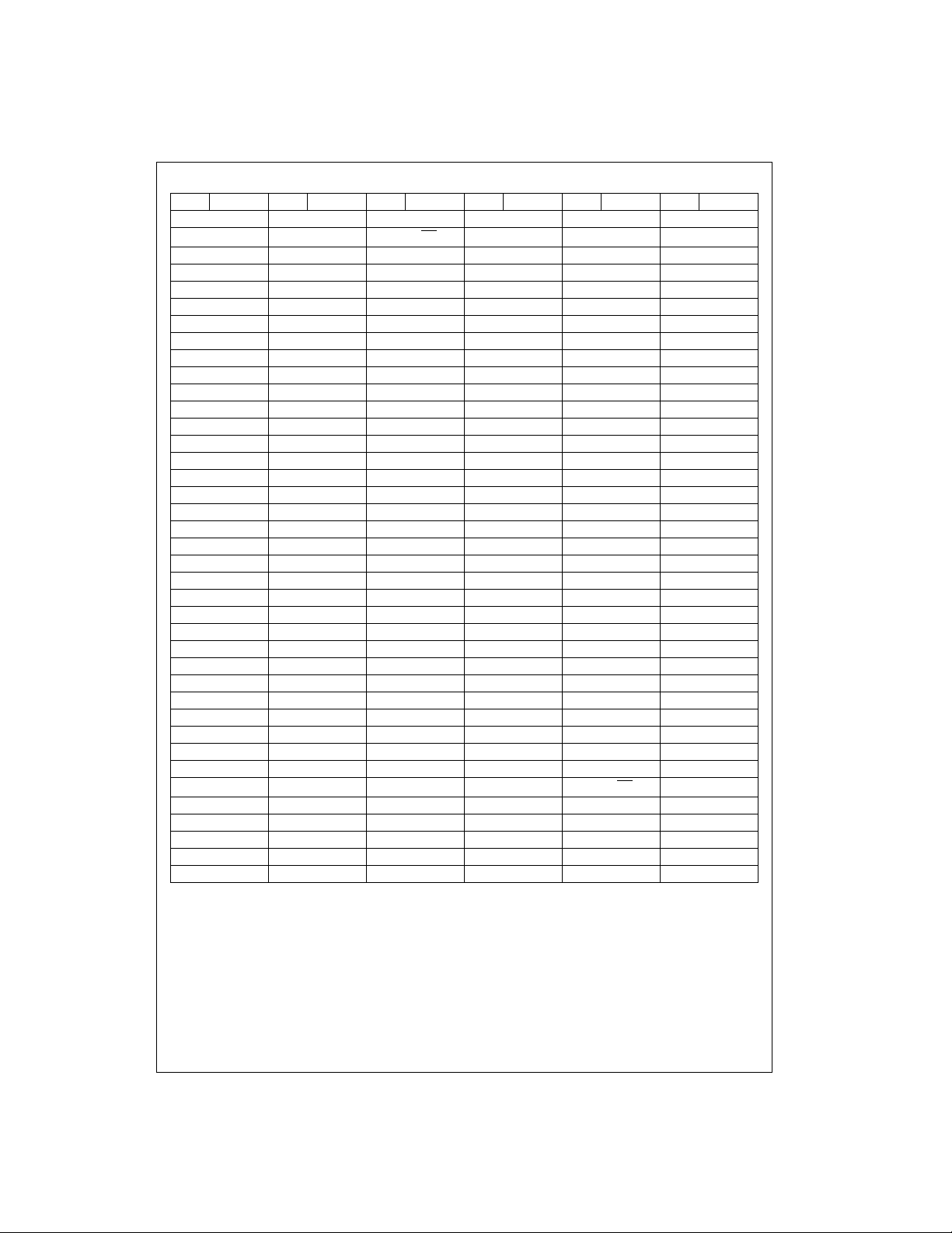
TABLE 10. MSX532 Pinout By Ball Sequence
Ball Ball Name Ball Ball Name Ball Ball Name Ball Ball Name Ball Ball Name Ball Ball Name
MSX532
A1 V
A2 V
A3 V
A4 V
A5 TRST
A6 P000 B6 P001 C6 TMS D6 RC_RDY E6 OE
A7 V
A8 P007 B8 P006 C8 P004 D8 P005 E8 V
A9 P012 B9 P013 C9 P010 D9 P011 E9 P008 F9 P009
A10 P016 B10 P017 C10 P015 D1 0 P014 E10 V
A11 V
A12 P026 B12 P024 C12 P025 D1 2 P023 E12 V
A13 P033 B13 P031 C13 P030 D13 P028 E13 P029 F13 P027
A14 P037 B14 P034 C14 P035 D1 4 P032 E14 V
A15 V
A16 P044 B16 P045 C16 P042 D1 6 P043 E16 V
A17 P050 B17 P051 C17 P048 D17 P049 E17 P047 F17 P046
A18 P055 B18 P054 C18 P052 D1 8 P053 E18 V
A19 V
A20 P065 B20 P060 C20 P063 D2 0 P062 E20 V
A21 V
A22 P071 B22 P070 C22 P072 D2 2 P073 E22 V
A23 P075 B23 P074 C23 P077 D23 P076 E23 P079 F23 P078
A24 P080 B24 P081 C24 P083 D2 4 P082 E24 V
A25 V
A26 P089 B26 P091 C26 P090 D2 6 P093 E26 V
A27 P092 B27 P095 C27 P094 D27 P096 E27 P097 F27 P099
A28 P098 B28 P100 C28 P101 D2 8 P103 E28 V
A29 V
A30 P109 B30 P108 C30 P11 1 D30 P110 E30 V
A31 P112 B31 P113 C31 P115 D31 P114 E31 P117 F31 P116
A32 P119 B32 P118 C32 P120 D32 P121 E32 V
A33 V
A34 P125 B34 P126 C34 P130 D3 4 P132 E34 P135 F34 V
A35 V
A36 V
A37 V
A38 V
A39 V
B1 V
SS
B2 V
SS
B3 V
SS
B4 CLK_0 C4 V
SS
B5 HW_RST C5 IE_0 D5 V
C1 V
SS
C2 V
SS
C3 V
SS
D1 V
SS
D2 RCA1 E2 RCA3 F2 RCA8
SS
D3 V
SS
D4 V
SS
E1 RCA6 F1 RCB1
SS
E3 RCA0 F3 RCA5
SS
E4 V
SS
E5 V
SS
SS
SS
_0 F6 V
B7 P002 C7 P003 D7 TCK E7 TDO F7 TDI
SS
DD
B11 P022 C11 P020 D11 P021 E11 P018 F11 P019
SS
B15 P040 C15 P041 D15 P039 E15 P038 F15 P036
SS
B19 P061 C19 P058 D19 P059 E19 P056 F19 P057
SS
B21 P064 C21 P066 D21 P067 E21 P069 F21 P068
SS
B25 P085 C25 P084 D25 P087 E25 P086 F25 P088
SS
B29 P102 C29 P104 D29 P105 E29 P107 F29 P106
SS
B33 P123 C33 P122 D33 P124 E33 P127 F33 P129
SS
B35 P128 C35 P133 D35 V
SS
B36 P131 C36 V
SS
SS
SS
SS
B37 V
B38 V
B39 V
SS
SS
SS
C37 V
C38 V
C39 V
SS
SS
SS
SS
D36 V
D37 V
D38 IE_1 E38 OE_1 F38 P139
D39 V
E35 V
SS
E36 V
SS
E37 P134 F37 CLK_1
SS
E39 P142 F39 P145
SS
DD
DD
DD
DD
DD
DD
DD
DD
DD
DD
DD
DD
SS
SS
F4 RCA4
F5 RCA2
F8 V
F10 V
F12 V
F14 V
F16 V
F18 V
F20 V
F22 V
F24 V
F26 V
F28 V
F30 V
F32 V
F35 P137
F36 P136
DD
DD
DD
DD
DD
DD
DD
DD
DD
DD
DD
DD
DD
DD
DD
www.fairchildsemi.com 26
Page 27
Package and Pinout (Continued)
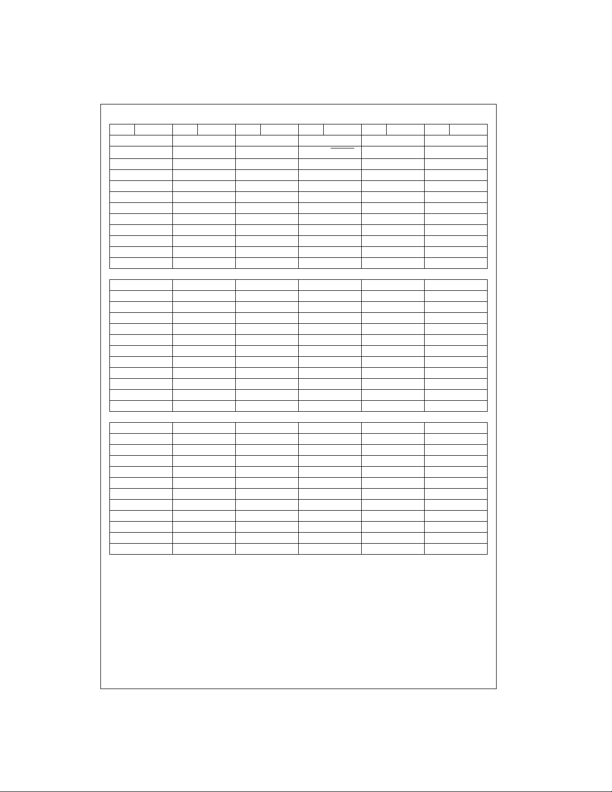
Ball Ball Name Ball Ball Name Ball Ball Name Ball Ball Name Ball Ball Name Ball Ball Name
G1 V
G2 RCB3 H2 RCB6 J2 RCC2 K2 RC_EN
G3 RCB2 H3 RCB5 J3 RCC1 K3 RC_CLK L3 P529 M3 P522
G4 RCB0 H4 RCB4 J4 RCC0 K4 RCI1 L4 P531 M4 P524
G5 RCA9 H5 V
G6 RCA7 H6 V
G34 P138 H34 V
G35 P141 H35 V
G36 P140 H36 P147 J36 P153 K36 P159 L36 P165 M36 P168
G37 P143 H37 P149 J37 P155 K37 P158 L37 P164 M37 P169
G38 P144 H38 P148 J38 P154 K38 P160 L38 P167 M38 P171
G39 P146 H39 P151 J39 V
H1 RCB7 J1 V
SS
K1 RCE L1 P526 M1 P521
SS
L2 P528 M2 P523
J5 RCB9 K5 RCI0 L 5 P530 M5 P525
DD
J6 RCB8 K6 RCC3 L6 UPDATE M6 P527
DD
J34 P150 K34 P157 L34 P163 M34 V
DD
J35 P152 K35 P156 L35 P162 M35 V
DD
K39 P161 L39 P166 M39 P170
SS
MSX532
DD
DD
N1 V
P1 P512 R1 V
SS
T1 P502 U1 V
SS
SS
V1 P495
N2 P517 P2 P513 R2 P506 T2 P504 U2 P499 V2 P494
N3 P516 P3 P515 R3 P509 T3 P505 U3 P498 V3 P496
N4 P519 P4 P514 R4 P508 T4 P507 U4 P501 V4 P497
N5 P518 P5 V
N6 P520 P6 V
N34 P172 P34 V
N35 P173 P35 V
R5 P511 T5 V
DD
R6 P510 T6 V
DD
R34 P180 T34 V
DD
R35 P183 T35 V
DD
U5 P500 V5 V
DD
U6 P503 V6 V
DD
U34 P190 V34 V
DD
U35 P192 V35 V
DD
DD
DD
DD
DD
N36 P175 P36 P177 R36 P182 T36 P186 U36 P193 V36 P197
N37 P174 P37 P179 R37 P184 T37 P189 U37 P195 V37 P196
N38 P176 P38 P178 R38 P185 T38 P188 U38 P194 V38 P199
N39 V
W1 P488 Y1 P485 AA1 V
P39 P181 R39 P187 T39 P191 U39 V
SS
AB1 P479 AC1 P475 AD1 P468
SS
SS
V39 P198
W2 P489 Y2 P484 AA2 P482 AB2 P476 AC2 P473 AD2 P466
W3 P491 Y3 P486 AA3 P478 AB3 P477 AC3 P472 AD3 P467
W4 P490 Y4 P487 AA4 P483 AB4 P474 AC4 P470 AD4 P465
W5 P492 Y5 V
W6 P493 Y6 V
W34 P200 Y34 V
W35 P201 Y35 V
AA5P481AB5 VDDAC5P471AD5 V
DD
AA6P480AB6 VDDAC6P469AD6 V
DD
AA34 P213 AB34 V
DD
AA35 P212 AB35 V
DD
AC34 P223 AD34 V
DD
AC35 P220 AD35 V
DD
DD
DD
DD
DD
W36 P203 Y36 P206 AA36 P210 AB36 P217 AC36 P221 AD36 P227
W37 P202 Y37 P207 AA37 P211 AB37 P216 AC37 P2 18 AD37 P225
W38 P205 Y38 P204 AA38 P209 AB38 P214 AC38 P219 AD38 P224
W39 V
Y39 P208 AA39 V
SS
AB39 P215 AC39 V
SS
SS
AD39 P222
27 www.fairchildsemi.com
Page 28
Package and Pinout (Continued)
Ball Ball Name Ball Ball Name Ball Ball Name Ball Ball Name Ball Ball Name Ball Ball Name
AE1 V
MSX532
AE2 P464 AF2 P459 AG2 P454 AH2 P449 AJ2 P447 AK2 P440
AE3 P462 AF3 P457 AG3 P455 AH3 P448 AJ3 P444 AK3 P438
AE4 P463 AF4 P456 AG4 P452 AH4 P446 AJ4 P445 AK4 P439
AE5P460AF5 V
AE6P461AF6 VDDAG6 V
AE34 P230 AF34 V
AE35 P231 AF35 V
AE36 P228 AF36 P234 AG36 P239 AH36 P245 AJ36 P246 AK36 P253
AE37 P229 AF37 P235 AG37 P236 AH37 P242 AJ37 P247 AK37 P252
AE38 P226 AF38 P233 AG38 P237 AH38 P243 AJ38 P244 AK38 P250
AE39 V
AF1 P458 AG1 P450 AH1 P451 AJ P443 AK1 P441
SS
DD
DD
DD
AF39 P232 AG39 V
SS
AG5 P453 AH5 V
AH6 V
SS
AG34 P240 AH34 V
AG35 P238 AH35 V
AH39 P241 AJ39 V
SS
AJ5 P442 AK5 V
DD
AJ6 V
DD
AJ34 P249 AK3 4 V
DD
AJ35 P248 AK3 5 V
DD
SS
SS
AK6 V
AK39 P251
DD
DD
DD
DD
AL1 P433 AM1 P432 AN1 V
SS
AL2 P436 AM2 P430 AN2 P429
AL3 P437 AM3 P431 AN3 P426
AL4 P434 AM4 P428 AN4 P427
AL5 P435 AM5 V
AL6 V
SS
AM6 V
AL34 P258 AM34 V
AL35 P259 AM35 V
DD
DD
DD
DD
AN5 P425
AN6 P423
AN34 P271
AN35 P268
AL36 P257 AM36 P262 AN36 P269
AL37 P256 AM37 P263 AN37 P267
AL38 P254 AM38 P260 AN38 P264
AL39 P255 AM39 P261 AN39 V
SS
www.fairchildsemi.com 28
Page 29
Package and Pinout (Continued)
Ball Ball Name Ball Ball Name Ball Ball Name Ball Ball Name Ball Ball Name Ball Ball Name
AP1 P424 AR1 V
AP2 P422 AR2 P421 AT2 OE_3 AU2 V
AP3 P420 AR3 P418 AT3 V
AP4 P419 AR4 V
AP5 V
AP6 V
AR5 V
DD
AR6 IE_3 AT6 P416 AU6 P414 AV6 P412 AW6 P407
DD
AP7 P413 AR7 P411 AT7 P409 AU7 P408 AV7 P406 AW7 V
AP8 P404 AR8 P405 AT8 P402 AU8 P403 AV8 P401 AW8 P400
AP9 P398 AR9 P399 AT9 P396 AU9 P397 AV9 P394 AW9 V
AP10 V
DD
AR10 V
AP11 P391 AR11 P389 AT11 P388 AU11 P386 AV11 V
AP12 V
DD
AR12 V
AP13 P380 AR13 P381 AT13 P378 AU13 P379 AV13 P377 AW13 V
AP14 V
DD
AR14 V
AP15 P373 AR15 P370 AT15 P371 AU15 P369 AV15 P368 AW15 P366
AP16 V
DD
AR16 V
AP17 P363 AR17 P361 AT17 P360 AU17 P358 AV17 P359 AW17 V
AP18 V
DD
AR18 V
AP19 P353 AR19 P352 AT19 P350 AU19 P351 AV19 P348 AW19 V
AP20 V
DD
AR20 V
AP21 P341 AR21 P340 AT21 P343 AU21 P342 AV21 P344 AW21 V
AP22 V
DD
AR22 V
AP23 P331 AR23 P330 AT23 P332 AU23 P333 AV23 P335 AW23 P334
AP24 V
DD
AR24 V
AP25 P321 AR25 P323 AT25 P322 AU25 P325 AV25 P324 AW25 V
AP26 V
DD
AR26 V
AP27 P310 AR27 P312 AT27 P313 AU27 P315 AV27 P314 AW27 P317
AP28 V
DD
AR28 V
AP29 P303 AR29 P302 AT29 P304 AU29 P305 AV29 P307 AW29 V
AP30 P296 AR30 P297 AT30 P299 AU30 P298 AV30 P301 AW30 P300
AP31 P290 AR31 P293 AT31 P292 AU31 P295 AV31 P294 AW31 V
AP32 V
DD
AR32 V
AP33 IE_2 AR33 P283 AT33 P282 AU33 P285 AV33 P2 87 AW33 V
AP34 V
AP35 V
AR34 P279 AT34 P281 AU34 P2 80 AV34 OE_2 AW34 P284
DD
AR35 V
DD
AP36 P2 74 AR36 V
AP37 P272 AR37 P277 AT37 V
AP38 P2 70 AR38 P273 AT38 P275 AU38 V
AP39 P265 AR39 P266 AT39 V
AT1 V
SS
AT4 V
SS
AT5 V
SS
AT10 P395 AU10 P393 AV10 P392 AW10 P390
DD
AT12 P385 AU12 P384 AV12 P382 AW12 P383
DD
AT14 P376 AU14 P374 AV14 P375 AW14 P372
DD
AT16 P367 AU16 P364 AV16 P365 AW16 P362
DD
AT18 P357 AU18 P356 AV18 P354 AW18 P355
DD
AT20 P346 AU20 P347 AV20 P349 AW20 P345
DD
AT22 P336 AU22 P337 AV22 P339 AW22 P338
DD
AT24 P327 AU24 P326 AV24 P328 AW24 P329
DD
AT26 P316 AU26 P319 AV26 P318 AW26 P320
DD
AT28 P306 AU28 P309 AV28 P308 AW28 P311
DD
AT32 P286 AU32 P289 AV32 P288 AW32 P291
DD
AT35 V
SS
AT36 V
SS
AU1 V
SS
AU3 V
SS
AU4 V
SS
AU5 P417 AV5 P4 15 AW5 P410
SS
AU35 P276 AV35 P278 AW35 CLK_2
SS
AU36 V
SS
AU37 V
SS
AU39 V
SS
AV1 V
SS
AV2 V
SS
AV3 V
SS
AV4 CLK_3 AW4 V
SS
AV36 V
SS
AV37 V
SS
AV38 V
SS
AV39 V
SS
SS
SS
SS
SS
SS
SS
SS
SS
AW1 V
AW2 V
AW3 V
AW11 P387
AW36 V
AW37 V
AW38 V
AW39 V
MSX532
SS
SS
SS
SS
SS
SS
SS
SS
SS
SS
SS
SS
SS
SS
SS
SS
SS
SS
29 www.fairchildsemi.com
Page 30
Package and Pinout (Continued)
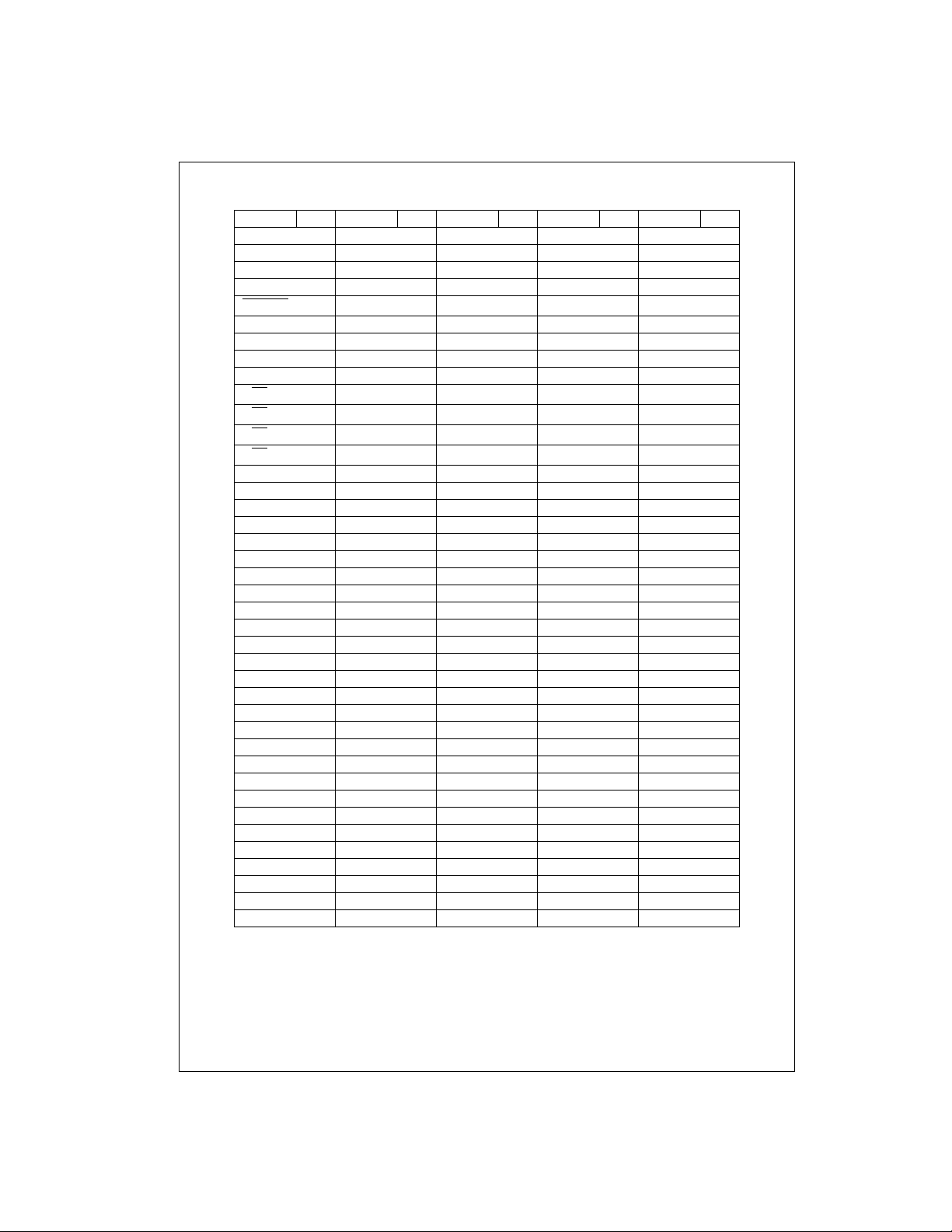
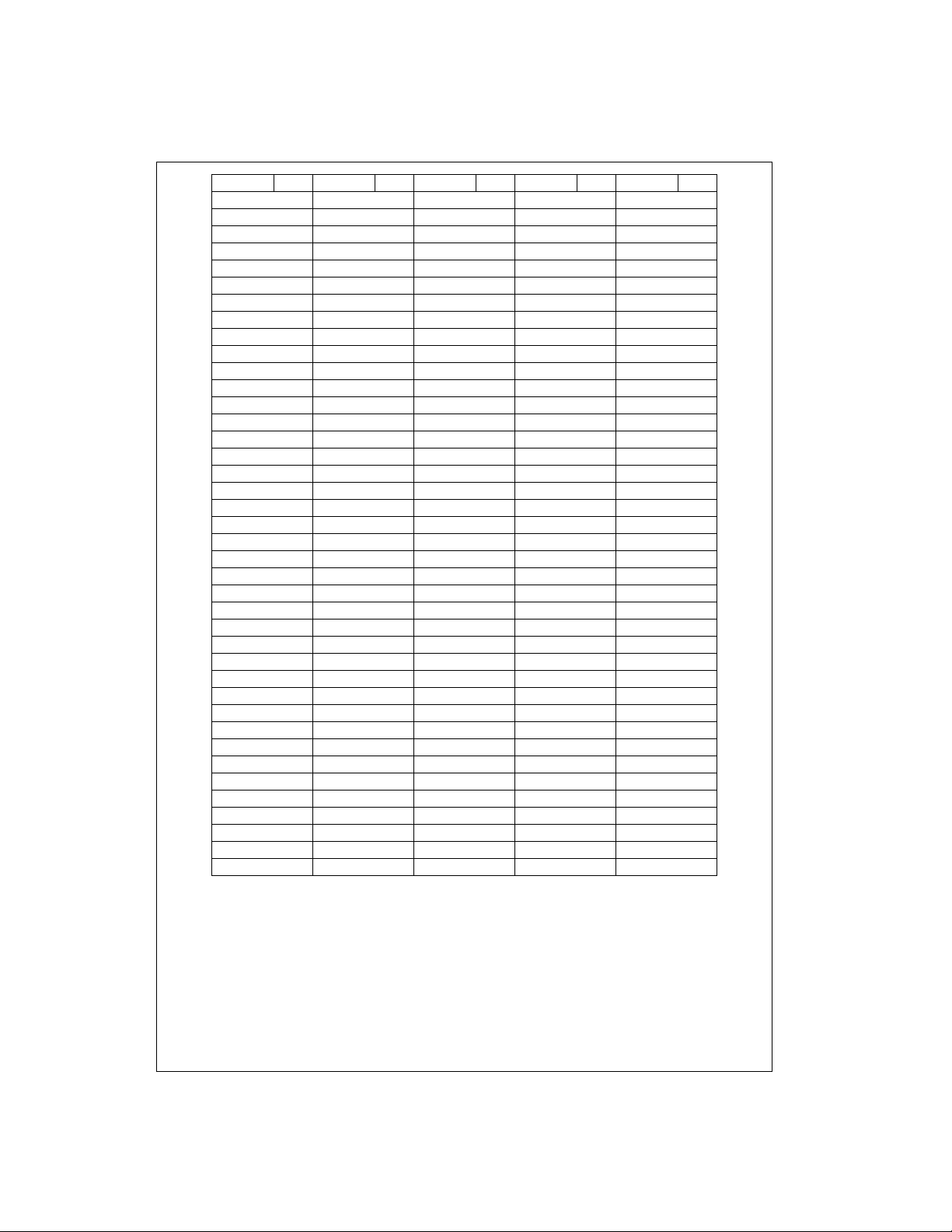
TABLE 11. MSX532 Pinout By Ball Name (alphabetically)
MSX532
Ball Name Ball Ball Name Ball Ball Name Ball Ball Name Ball Ball Name Ball
CLK_0 B4 P027 F13 P067 D21 P107 E29 P147 H36
CLK_1 F37 P028 D13 P068 F21 P108 B30 P148 H38
CLK_2 AW35 P029 E13 P069 E21 P109 A30 P149 H37
CLK_3 AV4 P030 C13 P070 B22 P110 D30 P150 J34
HW_RST
IE_0 C5 P032 D14 P072 C22 P112 A31 P152 J35
IE_1 D38 P033 A13 P073 D22 P113 B31 P153 J36
IE_2 AP33 P034 B14 P074 B23 P114 D31 P154 J38
IE_3 AR6 P035 C14 P075 A23 P115 C31 P155 J37
OE
OE
OE
OE
P000 A6 P040 B15 P080 A24 P120 C32 P160 K38
P001 B6 P041 C15 P081 B24 P121 D32 P161 K39
P002 B7 P042 C16 P082 D24 P122 C33 P162 L35
P003 C7 P043 D16 P083 C24 P123 B33 P163 L34
P004 C8 P044 A16 P084 C25 P124 D33 P164 L37
P005 D8 P045 B16 P085 B25 P125 A34 P165 L36
P006 B8 P046 F17 P086 E25 P126 B34 P166 L39
P007 A8 P047 E17 P087 D25 P127 E33 P167 L38
P008 E9 P048 C17 P088 F25 P128 B35 P168 M36
P009 F9 P049 D17 P089 A26 P129 F33 P169 M37
P010 C9 P050 A17 P090 C26 P130 C34 P170 M39
P011 D9 P051 B17 P091 B26 P131 B36 P171 M38
P012 A9 P052 C18 P092 A27 P132 D34 P172 N34
P013 B9 P053 D18 P093 D26 P133 C35 P173 N35
P014 D10 P054 B18 P094 C27 P134 E37 P174 N37
P015 C10 P055 A18 P095 B27 P135 E34 P175 N36
P016 A10 P056 E19 P096 D27 P136 F36 P176 N38
P017 B10 P057 F19 P097 E27 P137 F35 P177 P36
P018 E11 P058 C19 P098 A28 P138 G34 P178 P38
P019 F11 P059 D19 P099 F27 P139 F38 P179 P37
P020 C11 P060 B20 P100 B28 P140 G36 P180 R34
P021 D11 P061 B19 P101 C28 P141 G35 P181 P39
P022 B11 P062 D20 P102 B29 P142 E39 P182 R36
P023 D12 P063 C20 P103 D28 P143 G37 P183 R35
P024 B12 P064 B21 P104 C29 P144 G38 P184 R37
P025 C12 P065 A20 P105 D29 P145 F39 P185 R38
P026 A12 P066 C21 P106 F29 P146 G39 P186 T36
B5 P031 B13 P071 A22 P111 C30 P151 H39
_0 E6 P036 F15 P076 D23 P116 F31 P156 K35
_1 E38 P037 A14 P077 C23 P117 E31 P157 K34
_2 AV34 P038 E15 P078 F23 P118 B32 P158 K37
_3 AT2 P039 D15 P079 E23 P119 A32 P159 K36
www.fairchildsemi.com 30
Page 31
Ball Name Ball Ball Name Ball Ball Name Ball Ball Name Ball Ball Name Ball
P187 R39 P227 AD36 P267 AN37 P307 AV29 P347 AU20
P188 T38 P228 AE36 P268 AN35 P308 AV28 P348 AV19
P189 T37 P229 AE37 P269 AN36 P309 AU28 P349 AV20
P190 U34 P230AE34P270AP38P310AP27P350AT19
P191 T39 P231 AE35 P271 AN34 P311 AW28 P351 AU19
P192 U35 P232 AF39 P272 AP37 P312 AR27 P352 AR19
P193 U36 P233 AF38 P273 AR38 P313 AT27 P353 AP19
P194 U38 P234 AF36 P274 AP36 P314 AV27 P354 AV18
P195 U37 P235 AF37 P275 AT38 P315 AU27 P355 AW18
P196 V37 P236 AG37 P276 AU35 P316 AT26 P356 AU18
P197 V36 P237 AG38 P277 AR37 P317 AW27 P357 AT18
P198 V39 P238 AG35 P278 AV35 P318 AV26 P358 AU17
P199 V38 P239 AG36 P279 AR34 P319 AU26 P359 AV17
P200 W34 P240 AG34 P280 AU34 P320 AW26 P360 AT17
P201 W35 P241 AH39 P281 AT34 P321 AP25 P361 AR17
P202 W37 P242 AH37 P282 AT33 P322 AT25 P362 AW16
P203 W36 P243 AH38 P283 AR33 P323 AR25 P363 AP17
P204 Y38 P244 AJ38 P284 AW34 P324 AV25 P364 AU16
P205 W38 P245 AH36 P285 AU33 P325 AU25 P365 AV16
P206 Y36 P246 AJ36 P286 AT32 P326 AU24 P366 AW15
P207 Y37 P247 AJ37 P287 AV33 P327 AT24 P367 AT16
P208 Y39 P248 AJ35 P288 AV32 P328 AV24 P368 AV15
P209 AA38 P249 AJ34 P289 AU32 P329 AW24 P369 AU15
P210 AA36 P250 AK38 P290 AP31 P330 AR23 P370 AR15
P211 AA37 P251 AK39 P291 AW32 P331 AP23 P371 AT15
P212 AA35 P252 AK37 P292 AT31 P332 AT23 P372 AW14
P213 AA34 P253 AK36 P293 AR31 P333 AU23 P373 AP15
P214 AB38 P254 AL38 P294 AV31 P334 AW23 P374 AU14
P215 AB39 P255 AL39 P295 AU31 P335 AV23 P375 AV14
P216 AB37 P256 AL37 P296 AP30 P336 AT22 P376 AT14
P217 AB36 P257 AL36 P297 AR30 P337 AU22 P377 AV13
P218 AC37 P258 AL34 P298 AU30 P338 AW22 P378 AT13
P219 AC38 P259 AL35 P299 AT30 P339 AV22 P379 AU13
P220 AC35 P260 AM38 P300 AW30 P340 AR21 P380 AP13
P221 AC36 P261 AM39 P301 AV30 P341 AP21 P381 AR13
P222 AD39 P262 AM36 P302 AR29 P342 AU21 P382 AV12
P223 AC34 P263 AM37 P303 AP29 P343 AT21 P383 AW12
P224 AD38 P264 AN38 P304 AT29 P344 AV21 P384 AU12
P225 AD37 P265 AP39 P305 AU29 P345 AW20 P385 AT12
P226 AE38 P266 AR39 P306 AT28 P346 AT20 P386 AU11
MSX532
31 www.fairchildsemi.com
Page 32
MSX532
Ball Name Ball Ball Name Ball Ball Name Ball Ball Name Ball Ball Name Ball
P387 AW11 P427 AN4 P467 AD3 P507 T4 RCB3 G2
P388 AT11 P428 AM4 P468 AD1 P508 R4 RCB4 H4
P389 AR11 P429 AN2 P469 AC6 P509 R3 RCB5 H3
P390 AW10 P430 AM2 P470 AC4 P510 R6 RCB6 H2
P391 AP11 P431 AM3 P471 AC5 P511 R5 RCB7 H1
P392 AV10 P432 AM1 P472 AC3 P512 P1 RCB8 J6
P393 AU10 P433 AL1 P473 AC2 P513 P2 RCB9 J5
P394 AV9 P434 AL4 P474 AB4 P514 P4 RCC0 J4
P395 AT10 P435 AL5 P475 AC1 P515 P3 RCC1 J3
P396 AT9 P436 AL2 P476 AB2 P516 N3 RCC2 J2
P397 AU9 P437 AL3 P477 AB3 P517 N2 RCC3 K6
P398 AP9 P438 AK3 P478 AA3 P518 N5 RCE K1
P399 AR9 P439 AK4 P479 AB1 P519 N4 RCI0 K5
P400 AW8 P440 AK2 P480 AA6 P520 N6 RCI1 K4
P401 AV8 P441 AK1 P481 AA5 P521 M1 RC_RDY D6
P402 AT8 P442 AJ5 P482 AA2 P522 M3 TCK D7
P403 AU8 P443 AJ1 P483 AA4 P523 M2 TDI F7
P404 AP8 P444 AJ3 P484 Y2 P524 M4 TDO E7
P405 AR8 P445 AJ4 P485 Y1 P525 M5 TMS C6
P406 AV7 P446 AH4 P486 Y3 P526 L1 TRST
A5
P407 AW6 P447 AJ2 P487 Y4 P527 M6 UPDATE L6
P408 AU7 P448 AH3 P488 W1 P528 L2 V
P409 AT7 P449 AH2 P489 W2 P529 L3 V
P410 AW5 P450 AG1 P490 W4 P530 L5 V
P411 AR7 P451 AH1 P491 W3 P531 L4 V
P412 AV6 P452 AG4 P492 W5 RC_CLK K3 V
P413 AP7 P453 AG5 P493 W6 RC_EN
K2 V
P414 AU6 P454 AG2 P494 V2 RCA0 E3 V
P415 AV5 P455 AG3 P495 V1 RCA1 D2 V
P416 AT6 P456 AF4 P496 V3 RCA2 F5 V
P417 AU5 P457 AF3 P497 V4 RCA3 E2 V
P418 AR3 P458 AF1 P498 U3 RCA4 F4 V
P419 AP4 P459 AF2 P499 U2 RCA5 F3 V
P420 AP3 P460 AE5 P500 U5 RCA6 E1 V
P421 AR2 P461 AE6 P501 U4 RCA7 G6 V
P422 AP2 P462 AE3 P502 T1 RCA8 F2 V
P423 AN6 P463 AE4 P503 U6 RCA9 G5 V
P424 AP1 P464 AE2 P504 T2 RCB0 G4 V
P425 AN5 P465 AD4 P505 T3 RCB1 F1 V
P426 AN3 P466 AD2 P5 06 R2 RCB2 G3 V
DD
DD
DD
DD
DD
DD
DD
DD
DD
DD
DD
DD
DD
DD
DD
DD
DD
DD
DD
E8
E10
E12
E14
E16
E18
E20
E22
E24
E26
E28
E30
E32
F6
F8
F10
F12
F14
F16
www.fairchildsemi.com 32
Page 33
Ball Name Ball Ball Name Ball Ball Name Ball Ball Name Ball Ball Name Ball
DD
DD
DD
DD
DD
DD
DD
DD
DD
DD
DD
DD
DD
DD
DD
DD
DD
DD
DD
DD
DD
DD
DD
DD
DD
DD
DD
DD
DD
DD
DD
DD
DD
DD
DD
DD
DD
DD
DD
DD
F18 V
F20 V
F22 V
F24 V
F26 V
F28 V
F30 V
F32 V
F34 V
H5 V
H6 V
H34 V
H35 V
M34 V
M35 V
P5 V
P6 V
P34 V
P35 V
T5 V
T6 V
T34 V
T35 V
V5 V
V6 V
V34 V
V35 V
Y5 V
Y6 V
Y34 V
Y35 V
AB5 V
AB6 V
AB34 V
AB35 V
AD5 V
AD6 V
AD34 V
AD35 V
AF5 V
V
V
V
V
V
V
V
V
V
V
V
V
V
V
V
V
V
V
V
V
V
V
V
V
V
V
V
V
V
V
V
V
V
V
V
V
V
V
V
V
DD
DD
DD
DD
DD
DD
DD
DD
DD
DD
DD
DD
DD
DD
DD
DD
DD
DD
DD
DD
DD
DD
DD
DD
DD
DD
DD
DD
DD
DD
DD
DD
DD
DD
DD
DD
DD
DD
DD
DD
AF6 V
AF34 V
AF35 V
AH5 V
AH6 V
AH34 V
AH35 V
AK5 V
AK6 V
AK34 V
AK35 V
AM5 V
AM6 V
AM34 V
AM35 V
AP5 V
AP6 V
AP10 V
AP12 V
AP14 V
AP16 V
AP18 V
AP20 V
AP22 V
AP24 V
AP26 V
AP28 V
AP32 V
AP34 V
AP35 V
AR10 V
AR12 V
AR14 V
AR16 V
AR18 V
AR20 V
AR22 V
AR24 V
AR26 V
AR28 V
DD
SS
SS
SS
SS
SS
SS
SS
SS
SS
SS
SS
SS
SS
SS
SS
SS
SS
SS
SS
SS
SS
SS
SS
SS
SS
SS
SS
SS
SS
SS
SS
SS
SS
SS
SS
SS
SS
SS
SS
AR32 V
A1 V
A2 V
A3 V
A4 V
A7 V
A11 V
A15 V
A19 V
A21 V
A25 V
A29 V
A33 V
A35 V
A36 V
A37 V
A38 V
A39 V
B1 V
B2 V
B3 V
B37 V
B38 V
B39 V
C1 V
C2 V
C3 V
C4 V
C36 V
C37 V
C38 V
C39 V
D1 V
D3 V
D4 V
D5 V
D35 V
D36 V
D37 V
D39 V
SS
SS
SS
SS
SS
SS
SS
SS
SS
SS
SS
SS
SS
SS
SS
SS
SS
SS
SS
SS
SS
SS
SS
SS
SS
SS
SS
SS
SS
SS
SS
SS
SS
SS
SS
SS
SS
SS
SS
SS
E4 V
E5 V
E35 V
E36 V
G1 V
J1 V
J39 V
N1 V
N39 V
R1 V
U1 V
U39 V
W39 V
AA1 V
AA39 V
AC39 V
AE1 V
AE39 V
AG6 V
AG39 V
AJ6 V
AJ39 V
AL6 V
AN1 V
AN39 V
AR1 V
AR4 V
AR5 V
AR35 V
AR36 V
AT1 V
AT3 V
AT4
AT5
AT35
AT36
AT37
AT39
AU1
AU2
AU3
SS
AU4
SS
AU36
SS
AU37
SS
AU38
SS
AU39
SS
AV1
SS
AV2
SS
AV3
SS
AV11
SS
AV36
SS
AV37
SS
AV38
SS
AV39
SS
AW1
SS
AW2
SS
AW3
SS
AW4
SS
AW7
SS
AW9
SS
AW13
SS
AW17
SS
AW19
SS
AW21
SS
AW25
SS
AW29
SS
AW31
SS
AW33
SS
AW36
SS
AW37
SS
AW38
SS
AW39
SS
MSX532
33 www.fairchildsemi.com
Page 34
Package Thermal Characteristics
TABLE 12. Package Thermal Characteristics
MSX532
Package Pin Count
TBGA 792 0.4 7.58 6.00 5.66 5.26
Thermal per formance values are based on simulation data
θ
JC
(°C/W)
θ
(°C/W) θJA (°C/W) θJA (°C/W) θJA (°C/W)
JA
Still Air 200 Ifpm 300 Ifpm 500 Ifpm
Power Consumption
There are three components to consider when calculating power for the MSX Family of devices:
1. Steady State Component:
This element equals 252 mW.
2. Connection Component:
This element equals 0.006 mW x Mb/s x connections.
3. Output Drive Component:
This element equals 0.013 mW x number of outputs x Mb/s x capacitive load (pF).
Power Consumption = Steady State Component + Connection Component + Output Drive Component.
= 252 mW + (0.006 x Mb/s x #connections) + (0.013 x Mb/s x #outputs x Cload)
The following examples shows the total power consumption as determined by the above formula:
Example 1
Using the MSX532 with 10 Mb/s into a 10pF load with 266 inputs connected to 266 outputs:
Power Consumption
Example 2
Using the MSX532 with 150 Mb/s into a 10pF load with 266 inputs connected to 266 outputs:
Power Consumption
= 252 mW + (0.006 x 10 x 266) + (0.013 x 266 x 10 x 10)
= 2 52 mW + 16 mW + 346 mW = 0.614 Watts
= 252 mW + (0.006 x 150 x 266) + (0.013 x 266 x 150 x 10)
= 252 mW + 239.4 mW + 5187 mW = 5.68 Watts
Glossary
Array Side: The signal and connections between the Cros-
spoint Array and the I/O Buffer.
Bus Repeater: A circuit operation o f the I/O Buffer that
enables the MSX device to pass data in both directions on
an I/O device pin. The I/O Buffer is placed in a disabled
output state to the pin and to the Crosspoint array. A forced
LOW on either side of the I/O Buffer will be tran smitted to
the other side of the I/O Buffer and held until the forced
LOW is changed to a force HIGH. At the change of the
forcing input, the I/O Buffer will force the other side to a following high state and d rive a high level out for a period of
time. After the period o f time, the I/O Buffer will return to
the disabled state.
Bypass: A JTAG instruction that connects the previous
chip to the next chip through a one bit data register to
speed up progra mming of other chip s in a JTAG chain of
devices.
Clock: Four device corner inputs used to gate data into
registers in the I/O Buffer. The Corner inputs serve two
sides of the MSX. This provides two choices for each I/O
Buffer register in and reg ister out. The neig hbor input can
also be used as register clock and the clocks can be
inverted.
Control Register: A progr ammable register used to con trol various functions in progra mming an d other circuit settings. All Bits programmed in the JTAG Mode.
www.fairchildsemi.com 34
RapidConfigure Enab le bit can be set with a h igh level on
the RCE pin during a reset of the circuits.
Crosspoint: A single cell containing two N Channel tra nsistors and two RAM bits. The RAM bits are connected in a
master-slave configuration to provide an update for programming and chan ging program informat ion all at once.
Each cell contains both an X and Y rese t to remove all
ports connected to an addr essed port in a single progr am
cycle.
Crosspoint Array: An array of Crosspoint used to connect
any port to any othe r por t or an y comb inat io n of othe r por ts .
The array has all redun dant ce ll rem oved; th ere is a single
Crosspoint cell for each port to port connection. The
reduced cell count is f olded to provide a s quare array. The
array has a diagonal line where the cells are rotated.
Data Bit Lines: A pair of signal lines used to write into and
read out of Crosspoint Cells. The lines are pre-charged
before a read and one is pulled LOW for a write.
Device ID: A 32-bit register in the MSX device with a wired
identification. The ID consists of a given number for the
device and a revision history field. The identification is
shifted out during JTAG reset and the DEVICE ID instruction in JTAG mode. The ID for the MSX devices is
0x0000A89F.
Page 35

Glossary (Continued)
Extest: A JTAG instruction that sample s I/O p in sta tes a nd
loads new I/O buffer states for tes ting device pin connections. The MSX devices use a special tes t mode in Extext
to observe the buffer d ata on the pin side and the arr ay
side. A bit in the Control Register controls this mode.
I/O Buffer: The circuit that controls the driving of its associated pin and its port into and out of the Crosspoint Array.
The buffer contains all the circuits to make it independent
of the other I/O Buffers. E ach Buffer contai ns registers f or
input and output, driving circuits for input and output, sense
for Crosspoint Array input, and RAM bits to hold programmed data controlling the function of the buffer.
Input or Output Path: T he signal flow from pin to array
and array to pin. E ach path has a regi ster with selectabl e
clocks, drivers for the loaded outputs with selectable
enables, and sense circu its to detect changes on either
side of the I/O Buffer.
JTAG: The Joint Test Action group is a committ ee to standardize scan testing of devices. The JTAG interface is
referred to as IEEE 1149.1. This is a five bit serial programming and testing method.
JTAG Sequence: The ordering of all the pins in a serial
chain for driving and se nsing si gnals o n pins d uring E xtest
and Sample/Preload. All pins except power and ground
and the five JTAG pins are in the serial string.
Next Neighbor : Input can be selected as the clock for the
I/O buffer registers for data and clock pairing. The next
MSX532
higher port is t he selected neighbor except for Port 531,
which uses Port 0.
Pin Side Driver: The I/O Buffer circuit that drives the
device pin associated with that buffer.
Port: A name followed by a number t o ide ntify a pi n o n the
device. Ports are numbered from 531 to 0 on the MSX
device. In shifting sequence, Port P000 is shifted in first
and shifted out first.
RapidConfigure: A parallel programming method for the
MSX devices. Th e RC mode uses 29 dedi cate d pin s to pro gram the Crosspoint Array and the I/O Buffers. The 29 pins
consist of an enable, a strobe, two instruction bits, four
variable bits, and two ten-bit address fields.
RCE: A control pin of the MSX d evice that is samp led during reset to determine if the device beco mes active in the
JTAG or the RapidConfigure mode. This pin places the
Control Register bit i n the state to allow RC op erations or
not based on the volt age level of the RCE pin. The JTAG
mode is always enabled an d can set or clear the RC bit in
the Control Register.
Trickle Current: A very low current (~15 microamper es)
used to pull unused or n on -dr iv en circui t s to a stab le H IG H
level. Prevents signals from drifting between CMOS thresholds and drawing curr ents from the power supply. In the
case of Bus Repeater, the small trickle current provid es a
known high level on the pin and array side inputs.
35 www.fairchildsemi.com
Page 36
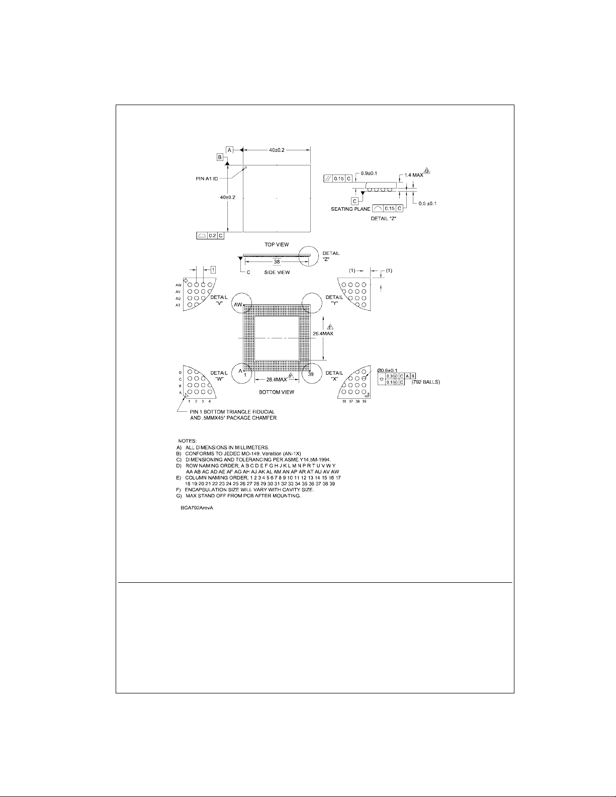
Physical Dimensions inches (millimeters) unless otherwise noted
MSX532 532 Port Digital Crosspoint Switch with LVTTL I/O’s
792-Ball Thermally-Enhanced Ball Grid Array (TBGA), JEDEC MO-149, 1.0mm pitch, 40mm Square
Fairchild does not assume any responsibility for use of any circuitr y described, no circuit patent licenses are implied a nd
Fairchild reserves the right at any time without notice to change said circuitry and specifications.
LIFE SUPPORT POLICY
FAIRCHILD’S PRODUCTS ARE NOT AUTHORIZED FOR USE AS CRITICAL COMPONENTS IN LIFE SUPPORT
DEVICES OR SYSTEMS WITHOUT THE EXPRESS WRITTEN APPROVAL OF THE PRESIDENT OF FAIRCHILD
SEMICONDUCTOR CORPORATION. As used herein:
1. Life support devices or systems are devices or systems
which, (a) are intended for surgical implant into the
body, or (b) support or sustain life, and (c) whose failure
to perform when properly used in accordance with
instructions for use provided in the labeling, can be reasonably expected to result in a significant inju ry to the
user.
www.fairchildsemi.com 36
Package Number BGA792A
2. A critical component in any compon ent of a lif e supp ort
device or system whose failu re to perform can be reasonably expected to cause the failure of the li fe su pp ort
device or system, or to affect its safety or effectiveness.
www.fairchildsemi.com
 Loading...