

Page 1
MSP 34x5G
Multistandard
Sound Processor Family
Edition Jan. 19, 2001
6251-480-3PD
PRELIMINARY DATA SHEET
MICRONAS
MICRONAS
Page 2

MSP 34x5G PRELIMINARY DATA SHEET
Contents
Page Section Title
5 1. Introduction
6 1.1. Features of the MSP 34x5G Family and Differences to MSPD
6 1.2. MSP 34x5G Version List
7 1.3. MSP 34x5G Versions and their Application Fields
8 2. Functional Description
9 2.1. Architecture of the MSP 34x5G Family
9 2.2. Sound IF Processing
9 2.2.1. Analog Sound IF Input
9 2.2.2. Demodulator: Standards and Features
10 2.2.3. Preprocessing of Demodulator Signals
10 2.2.4. Automatic Sound Select
10 2.2.5. Manual Mode
2
12 2.3. Preprocessing for SCART and I
12 2.4. Source Selection and Output Channel Matrix
12 2.5. Audio Baseband Processing
12 2.5.1. Automatic Volume Correction (AVC)
12 2.5.2. Loudspeaker Outputs
12 2.5.3. Quasi-Peak Detector
13 2.6. SCART Signal Routing
13 2.6.1. SCART DSP In and SCART Out Select
13 2.6.2. Stand-by Mode
2
13 2.7. I
S Bus Interface
14 2.8. ADR Bus Interface
14 2.9. Digital Control I/O Pins and Status Change Indication
14 2.10. Clock PLL Oscillator and Crystal Specifications
S Input Signals
15 3. Control Interface
2
15 3.1. I
C Bus Interface
15 3.1.1. Internal Hardware Error Handling
16 3.1.2. Description of CONTROL Register
16 3.1.3. Protocol Description
2
17 3.1.4. Proposals for General MSP 34x5G I
C Telegrams
17 3.1.4.1. Symbols
17 3.1.4.2. Write Telegrams
17 3.1.4.3. Read Telegrams
17 3.1.4.4. Examples
2
17 3.2. Start-Up Sequence: Power-Up and I
C-Controlling
17 3.3. MSP 34x5G Programming Interface
17 3.3.1. User Registers Overview
20 3.3.2. Description of User Registers
21 3.3.2.1. STANDARD SELECT Register
21 3.3.2.2. Refresh of STANDARD SELECT Register
21 3.3.2.3. STANDARD RESULT Register
2
23 3.3.2.4. Write Registers on I
25 3.3.2.5. Read Registers on I2C Subaddress 11
26 3.3.2.6. Write Registers on I2C Subaddress 12
C Subaddress 10
hex
hex
hex
2 Micronas
Page 3

PRELIMINARY DATA SHEET
Contents, continued
Page Section Title
MSP 34x5G
36 3.3.2.7. Read Registers on I2C Subaddress 13
37 3.4. Programming Tips
37 3.5. Examples of Minimum Initialization Codes
37 3.5.1. B/G-FM (A2 or NICAM)
37 3.5.2. BTSC-Stereo
37 3.5.3. BTSC-SAP with SAP at Loudspeaker Channel
38 3.5.4. FM-Stereo Radio
38 3.5.5. Automatic Standard Detection
38 3.5.6. Software Flow for Interrupt driven STATUS Check
40 4. Specifications
40 4.1. Outline Dimensions
42 4.2. Pin Connections and Short Descriptions
45 4.3. Pin Description
47 4.4. Pin Configurations
51 4.5. Pin Circuits
53 4.6. Electrical Characteristics
53 4.6.1. Absolute Maximum Ratings
54 4.6.2. Recommended Operating Conditions
54 4.6.2.1. General Recommended Operating Conditions
54 4.6.2.2. Analog Input and Output Recommendations
55 4.6.2.3. Recommendations for Analog Sound IF Input Signal
56 4.6.2.4. Crystal Recommendations
57 4.6.3. Characteristics
57 4.6.3.1. General Characteristics
58 4.6.3.2. Digital Inputs, Digital Outputs
59 4.6.3.3. Reset Input and Power-Up
60 4.6.3.4. I
61 4.6.3.5. I
63 4.6.3.6. Analog Baseband Inputs and Outputs, AGNDC
64 4.6.3.7. Sound IF Input
64 4.6.3.8. Power Supply Rejection
65 4.6.3.9. Analog Performance
68 4.6.3.10. Sound Standard Dependent Characteristics
2
C Bus Characteristics
2
S-Bus Characteristics
hex
72 5. Appendix A: Overview of TV Sound Standards
72 5.1. NICAM 728
73 5.2. A2 Systems
74 5.3. BTSC-Sound System
74 5.4. Japanese FM Stereo System (EIA-J)
75 5.5. FM Satellite Sound
75 5.6. FM-Stereo Radio
76 6. Appendix B: Manual/Compatibility Mode
76 6.1. Demodulator Write and Read Registers for Manual/Compatibility Mode
77 6.2. DSP Write and Read Registers for Manual/Compatibility Mode
78 6.3. Manual/Compatibility Mode: Description of Demodulator Write Registers
78 6.3.1. Automatic Switching between NICAM and Analog Sound
Micronas 3
Page 4

MSP 34x5G PRELIMINARY DATA SHEET
Contents, continued
Page Section Title
78 6.3.1.1. Function in Automatic Sound Select Mode
78 6.3.1.2. Function in Manual Mode
80 6.3.2. A2 Threshold
80 6.3.3. Carrier-Mute Threshold
81 6.3.4. Register AD_CV
82 6.3.5. Register MODE_REG
84 6.3.6. FIR-Parameter, Registers FIR1 and FIR2
84 6.3.7. DCO-Registers
86 6.4. Manual/Compatibility Mode: Description of Demodulator Read Registers
86 6.4.1. NICAM Mode Control/Additional Data Bits Register
86 6.4.2. Additional Data Bits Register
86 6.4.3. CIB Bits Register
87 6.4.4. NICAM Error Rate Register
87 6.4.5. PLL_CAPS Readback Register
87 6.4.6. AGC_GAIN Readback Register
87 6.4.7. Automatic Search Function for FM-Carrier Detection in Satellite Mode
88 6.5. Manual/Compatibility Mode: Description of DSP Write Registers
88 6.5.1. Additional Channel Matrix Modes
88 6.5.2. Volume Modes of SCART1 Output
88 6.5.3. FM Fixed Deemphasis
88 6.5.4. FM Adaptive Deemphasis
88 6.5.5. NICAM Deemphasis
89 6.5.6. Identification Mode for A2 Stereo Systems
89 6.5.7. FM DC Notch
89 6.6. Manual/Compatibility Mode: Description of DSP Read Registers
89 6.6.1. Stereo Detection Register for A2 Stereo Systems
89 6.6.2. DC Level Register
90 6.7. Demodulator Source Channels in Manual Mode
90 6.7.1. Terrestric Sound Standards
90 6.7.2. SAT Sound Standards
90 6.8. Exclusions of Audio Baseband Features
90 6.9. Compatibility Restrictions to MSP 34x5D
92 7. Appendix D: Application Information
92 7.1. Phase Relationship of Analog Outputs
93 7.2. Application Circuit
94 8. Appendix E: MSP 34x5G Version History
94 9. Data Sheet History
License Notice:
“Dolby Pro Logic” is a trademark of Dolby Laboratories.
Supply of this implementation of Dolby Technology does not convey a license nor imply a right under any patent, or any other industrial or intellectual property right of Dolby Laboratories, to use this implementation in any finished end-user or ready-to-use final product. Companies planning to
use this implementation in products must obtain a license from Dolby Laboratories Licensing Corporation before designing such products.
4 Micronas
Page 5
PRELIMINARY DATA SHEET MSP 34x5G
Multistandard Sound Processor Family
Release Note: Revision bars indicate significant
changes to the previous edition. The hardware and
software description in this document is valid for
the MSP 34x5G version B8 and following versions.
1. Introduction
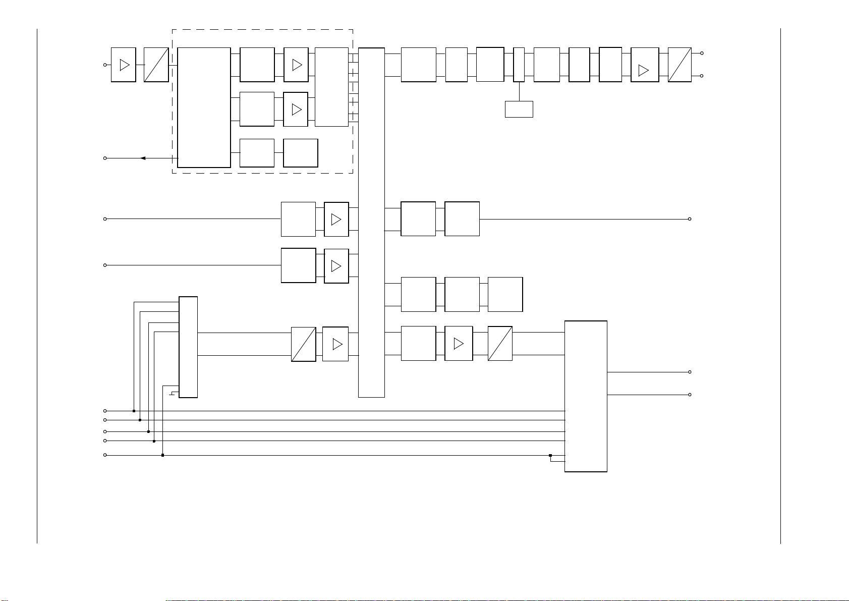
The MSP 34x5G family of single-chip Multistandard
Sound Processors covers the sound processing of all
analog TV standards worldwide, as well as the NICAM
digital sound standards. The full TV sound processing,
starting with analog sound IF signal-in, down to processed analog AF-out, is performed in a single chip.
Figure 1–1 shows a simplified functional block diagram
of the MSP 34x5G.
These TV sound processing ICs include versions for
processing the multichannel television sound (MTS)
signal conforming to the standard recommended by
the Broadcast Television Systems Committe e (BTSC).
The DBX noise reduction, or alternatively, Micronas
Noise Reduction (MNR) is performed alignment free.
Other processed standards are the Japanese FM-FM
multiplex standard (EIA-J) and the FM-Stereo-Radio
standard.
Current ICs have to perform adjustment p rocedures in
order to achieve good stereo separatio n for BTSC and
EIA-J. The MSP 34x5G has optimum stereo performance without any adjustments.
All MSP 34xxG versions are pin compatible to the
MSP 34xxD. Only minor modifications are necessary
to adapt a MSP 34xxD controlling software to the
MSP 34xxG. The MSP 34x5G further simplifies controlling software. St andard selection requi res a single
2
C transmission only.
I
Note: The MSP 34x5G version has reduced control
registers and less functional pins. The remaining registers are software-compatible to the MSP 34x0G. The
pinning is compatible to the MSP 34x0G.
The MSP 34x5G has built-in automatic functions: The
IC is able to detect the actual sound standard automatically (Automatic Standard Detection). Furthermore,
pilot levels and identification sign als can be evaluated
internally with subsequent switching between mono/
stereo/bilingual; no I
2
C interaction is ne cessar y (Auto-
matic Sound Selectio n) .
The MSP 34x5G can handle very high FM deviation s
even in conjunction with NICAM processing. This is
especially impor tant for the introduction of NICAM in
China.
The ICs are produced in submicron CMOS technology.
The MSP 34x5G is available in the following packages:
PSDIP64, PSDIP52, PMQFP44, PLQFP64, and
PQFP80.
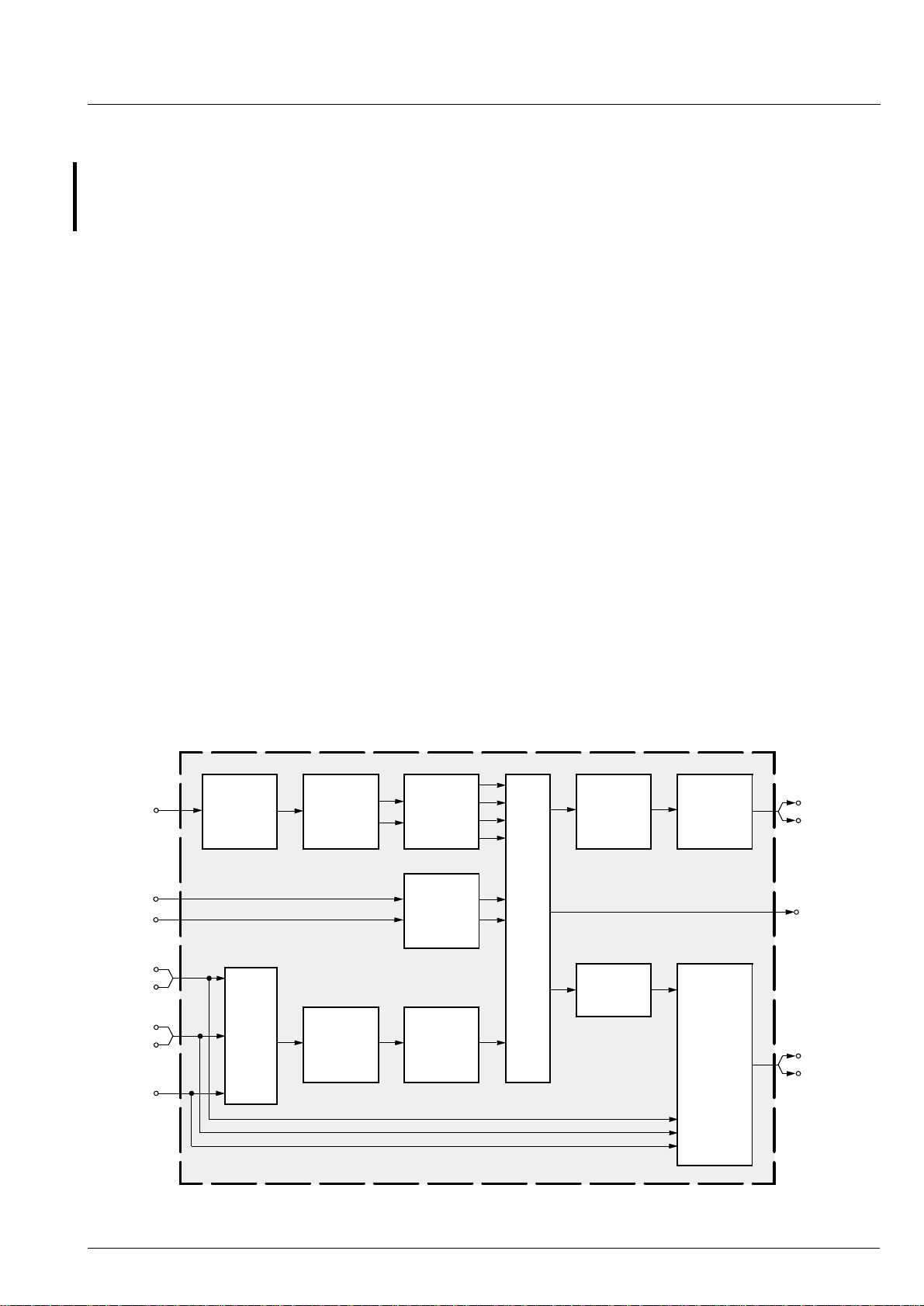
Sound IF1
I2S1
I2S2
SCART1
SCART2
MONO
SCART
DSP
Input
Select
De-
modulator
ADC
Pre-
processing
Prescale
Prescale
Fig. 1–1: Simplified functional block diagram of MSP 34x5G
Loud-
speaker
Sound
Processing
Source Select
DAC
DACADC
SCART
Output
Select
Loudspeaker
I2S
SCART1
Micronas 5
Page 6
MSP 34x5G PRELIMINARY DATA SHEET
1.1. Features of the MSP 34x5G Family and Differences to MSPD
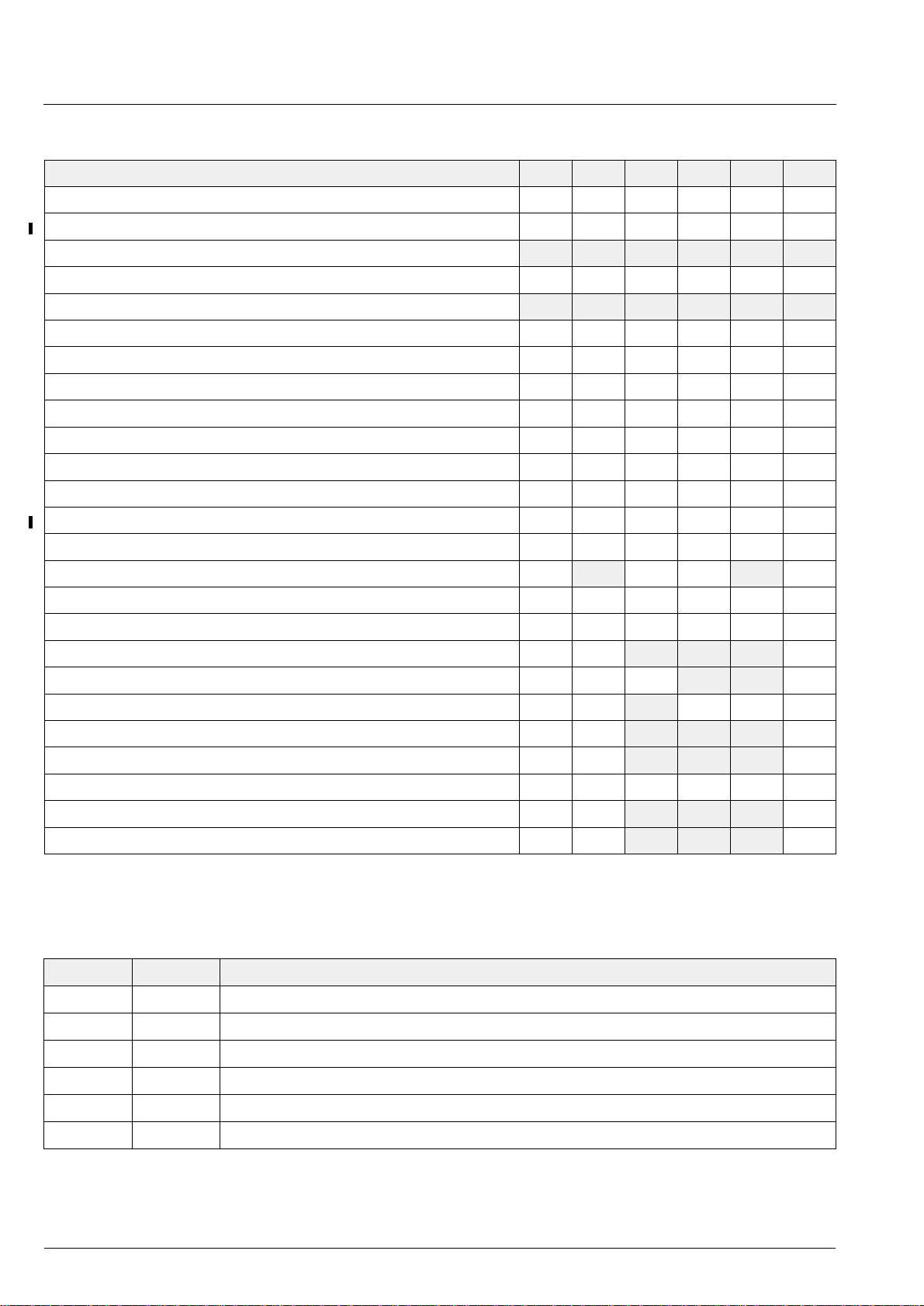
Feature (New features not available for MSPD are shaded gray. ) 3405 3415 3425 3445 3455 3465
Standard Selection with single I
Automatic Standard Detection of terrestrial TV standards X X X X X X
2
C transmission X X X X X X
Automatic Sound Selection (mono/stereo/bilingual), new registers MODUS, STATUS
Automatic Carrier Mute function X X X X X X
Interrupt output programmable (indicating status change)
Loudspeaker channel with volume, balance, bass, treble, loudness X X X X X X
AVC: Automatic Volume Correction X X X X X X
Spatial effect for loudspeaker channel X X X X X X
Two Stereo SCART (line) inputs, one Mono input; one Stereo SCART outputs X X X X X X
Complete SCART in/out switching matrix X X X X X X
2
S inputs; one I2S output X X X X X X
Two I
All analog Mono sound carriers including AM-SECAM L
All analog FM-Stereo A2 and satellite standards X X X
All NICAM standards XX
Simultaneous demodulation of (very) high-deviation FM-Mono and NICAM
Adaptive deemphasis for satellite (Wegener-Panda, acc. to ASTRA specification) X X X X
ASTRA Digital Radio (ADR) together with DRP 3510A X X X
Demodulation of the BTSC multiplex signal and the SAP channel
Alignment free digital DBX noise reduction for BTSC Stereo and SAP
X X X X X X
X X X X X X
X X X X X X
X X
X X X
X X
Alignment free digital Micronas Noise Reduction (MNR) for BTSC Stereo and SAP
BTSC stereo separation (MSP 3425/45G also EIA-J) significantly better than spec.
SAP and stereo detection for BTSC system
Korean FM-Stereo A2 standard X X X X X
Alignment-free Japanese standard EIA-J
Demodulation of the FM-Radio multiplex signal
X
X X X
X X X
X X X
X X X
1.2. MSP 34x5G Version List
Version Status Description
MSP 3405G available FM Stereo (A2) Version
MSP 3415G available NICAM and FM Stereo (A2) Version
MSP 3425G available NTSC Version (A2 Korea, BTSC with Micronas Noise Reduction (MNR), Japanese EIA-J system)
MSP 3445G available NTSC Version (A2 Korea, BTSC with DBX noise reduction, Japanese EIA-J system)
MSP 3455G available Global Stereo Version (all sound standards)
MSP 3465G available Global Mono Vers io n (all sound standards)
6 Micronas
Page 7
PRELIMINARY DATA SHEET MSP 34x5G
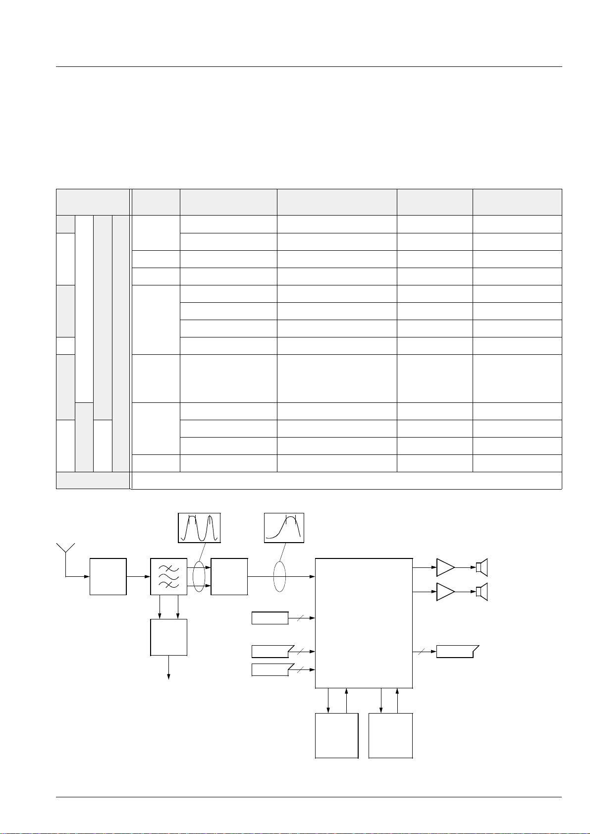
1.3. MSP 34x5G Versions and their Application Fields
Table 1–1 provides an overview of TV sound standards
that can be processed by the MSP 34x5G family. In
addition, the MSP 34x5G is able to handle the FMRadio standard. With the MSP 34x5G, a complete
multimedia receiver covering all TV sound standards
together with te rrestr ial/ cable and satel lite radio sou nd
can be built; even ASTRA Digital Radio can be processed (with a DRP 3510A coprocessor).
Table 1–1: TV Stereo Sound Standards covered by the MSP 34x5G IC Family (details see Appendix A)
MSP Version TV-
3405
3405
3405
3415
System
B/G
L 6.5/5.85 AM-Mono/NICAM SECAM-L France
I 6.0/6.552 FM-Mono/NICAM PAL UK, Hong Kong
D/K
3455
Satellite
Position of Sound
Carrier /MHz
5.5/5.7421875 FM-Stereo (A2) PAL Germany
5.5/5.85 FM-Mono/NICAM PAL Scandinavia, Spain
6.5/6.2578125 FM-Stereo (A2, D/K1) SECAM-East Slovak. Rep.
6.5/6.7421875 FM-Stereo (A2, D/K2) PAL currently no broadcast
6.5/5.7421875 FM-Stereo (A2, D/K3) SECAM-East Poland
6.5/5.85 FM-Mono/NICAM (D/K, NICAM) PAL China, Hungary
6.5
7.02/7.2
7.38/7.56
etc.
Sound
Modulation
FM-Mono
FM-Stereo
ASTRA Digital Radio (ADR)
with DRP 3510A
Color
System
PAL
Broadcast e.g. in:
Europe Sat.
ASTRA
4.5/4.724212 FM-Stereo (A2) NTSC Korea
M/N
3425, 3445
FM-Radio 10.7 FM-Stereo Radio USA, Europe
3465 All standards as above, but Mono demodulation only.
SAW Filter
Tuner
Composite
Video
4.5 FM-FM (EIA-J) NTSC Japan
4.5 BTSC-Stereo + SAP NTSC, PAL USA, Argentina
33 34 39 MHz 4.5 9 MHz
Sound
IF
Mixer
1
2
2
Vision
Demodulator
SCART
Inputs
Mono
SCART1
SCART2
MSP 34x5G
2
I
S1 ADR I2S2
2
SCART1
Loudspeaker
SCART Output
Dolby
Pro Logic
Processor
DPL 351xA
ADR
Decoder
DRP 3510A
Fig. 1–2: Typical MSP 34x5G application
Micronas 7
Page 8
8 Micronas
ANA_IN1+
ADR-Bus
Interface
AGC
A
D
Standard Selection
DEMODULATOR
(incl. Carrier Mute)
Decoded
Standards:
− NICAM
− A2
− AM
− BTSC
− EIA-J
− SAT
− FM-Radio
Deemphasis:
50/75 µs,
J17
DBX/MNR
Panda1
Deemphasis
J17
Standard
and Sound
Detection
FM/AM
Prescale
(0E
NICAM
Prescale
(10
I2C
Read
Register
Sound Select
)
hex
)
hex
Automatic
FM/AM
Stereo or A/B
Stereo or A
Stereo or B
2. Functional Description
0
1
3
Loud-
speaker
Channel
Matrix
(08
AVC
)
hex
Bass/
Treble
)
(02
hex
)
hex
)
(03
hex
Loud-
Σ
ness
(04
hex
Spatial
Effects
)(05
)(01
hex
Balance
Volume
)
(00
hex
D
)(29
hex
DACM_L
A
DACM_R
MSP 34x5G PRELIMINARY DATA SHEET
Beeper
4
(14
)
hex
I2S_DA_IN1
I2S_DA_IN2
I2S
Interface
I2S
Interface
I2S1
Prescale
(16
I2S2
5
)
hex
Source Select
6
I2S
Channel
Matrix
(0B
I2S
Interface
)
hex
Prescale
(12
)
hex
SCART
A
D
Prescale
2
(0D
)
hex
Quasi-Peak
Channel
Matrix
(0C
hex
SCART1
Channel
Matrix
(0A
hex
Quasi-Peak
Detector
)
Volume
)(07
)
hex
I2C
Read
Register
D
A
(19
(1A
SCART DSP Input Select
(13
)
hex
SC1_IN_L
SC1_IN_R
SC2_IN_L
SC2_IN_R
MONO_IN
ig. 2–1: Signal flow block diagram of the MSP 34x5G (input and output names correspond to pin names).
I2S_DA_OUT
)
hex
)
hex
SCART1_L/R
SC1_OUT_L
SC1_OUT_R
SCART Output Select
)
(13
hex
Page 9

PRELIMINARY DATA SHEET MSP 34x5G
2.1. Architecture of the MSP 34x5G Family
Fig. 2–1 on page 8 shows a simplified block diagram of
the IC. The block diagram contains all features of the
MSP 3455G. Other members of the MSP 34x5G family
do not have the complete set of features: The demodulator handles only a subset of the standards presented
in the demodulator block; NICAM processing is only
possible in the MSP 3415G and MSP 3455G (see
dashed block in Fig. 2–1).
2.2. Sound IF Processing
2.2.1. Analog Sound IF Input
The input pins ANA_ IN1+ and ANA _IN− offer the possibility to connect sound IF (SIF) sources to the
MSP 34x5G. The analog-to-digital conversion of the
sound IF signal is done by an A/D-conver ter. An analog automatic gain circuit (AGC) allows a wide range of
input levels. The high-pass filter formed by the coupling capacitor at pin ANA_IN1+ (see Section 7.
“Appendix D: Application Information” on page 92) is
sufficient in most cases to suppress video components. Some combinations of SAW filters and sound IF
mixer ICs, however, show large picture components on
their outputs. In this case, further filtering is recommended.
BTSC-Mono + SAP: Detection and FM demodulation
of the aural carrier resulting in the MTS/MPX signal.
Detection and evaluation of the pilot car rier, detection
and FM demodulat ion of the SA P-sub carr ier. Processing of the DBX noise reduction or Micronas Noise
Reduction (MNR).
Japan Stereo: Detection and FM demodulation of the
aural carrier resulting in the MPX signal. Demodulation
and evaluation of the identification signal and FM
demodulation of the (L-R)-carrier.
FM-Satellite Sound: Demodulation of one or two FM
carriers. Processi ng of high-deviation mono or na rrow
bandwidth mono, stereo, or bilingual satellite sound
according to the ASTRA specification.
FM-Stereo-Radio: Detection and FM demodulation of
the aural carrier resu lting in the MPX si gnal. Detecti on
and evaluation of the pilot carrier and AM demodulation of the (L-R)-carrier.
The demodulator blocks of all MSP 34x5G versions
have identical user interfaces. Even completely different systems like the BTSC and NICAM systems are
controlled the same way. Standards are selected by
means of MSP Standard Cod es. Automatic processes
handle standard detection and identification without
controller interaction. The key features of the
MSP 34x5G demodulator blocks are
2.2.2. Demodulator: Standards and Features
The MSP 34x5G is able to demodulate all TV sound
standards worldwide inc luding the digital NICAM system. Depending on the MSP 34x5G version, the following demodulation modes can be performed:
A2-Systems: Detectio n and demodu lation of two separate FM carriers ( FM1 and FM2), demodulation and
evaluation of the identification signal of carrier FM2.
NICAM-Systems: Demodulation and decoding of the
NICAM carrier, detection and demodulation of the analog (FM or AM) carrier. For D/K-NICAM, the FM carrier
may have a maximum deviation of 384 kHz.
Very high deviation FM-Mono: Detection and robust
demodulation of on e FM carr ier with a maximum deviation of 540 kHz.
BTSC-Stereo: Detection and FM demodulation of the
aural carrier resulting in the MTS/MPX signal. Detection and evaluation of the pilot carr ier, AM demodulation of the (L-R)-carr ier and detec tion of the SA P subcarrier. Processing of the DBX noise reduction or
Micronas Noise Reduction (MNR).
Standard Selection: The controlling of the de modula tor is minimized: All parameters, such as tuning frequencies or filter bandwidth, are adjusted automatically by transmitting one single value to the
STANDARD SELECT reg ister. For all standards, specific MSP standard codes are defined.
Automatic Standard Detection: If the TV sound standard is unknown, the MSP 34x5G can automatically
detect the actual standard, switch to that standard, and
respond the actual MSP standard code.
Automatic Carrier Mute: To prevent noise effects or
FM identification problems in the absence of an FM
carrier, the MSP 34x5G offers a configurable carrier
mute feature, which is activated automatically if th e T V
sound standard is selected by means of the STANDARD SELECT register. If no FM carrier is detected at
one of the two MSP demodulator channels, the corresponding demodulator output is muted. This is indicated in the STATUS register.
Micronas 9
Page 10
MSP 34x5G PRELIMINARY DATA SHEET
2.2.3. Preprocessing of Demodulator Signals
The NICAM signals must be processed by a deemphasis filter and adjusted in level. The analog demodulated signals must b e processed by a deemphas is filter, adjusted in level, and dematrixed. The correct
deemphasis filters are already selected by setting th e
standard in the STANDARD SELECT register. The
level adjustment has to be done by means of the FM/
AM and NICAM prescale registers. The necessary
dematrix function depends on the selected sound
standard and the actual broadcasted sound mode
(mono, stereo, or bilingual). It can be manually set by
the FM Matrix Mode register or automatically by the
Automatic Sound Selection.
2.2.4. Automatic Sound Select
In the Automatic Sound Select mode, the dematrix
function i s aut om a t ica l ly s el ec t ed ba se d on th e id ent if i cation information in the ST ATUS register. No I
2
C interaction is necessary when the broadcasted sound
mode changes (e.g. from mono to stereo).
The demodulator sup ports the identification ch eck by
switching between mono-compatible standards (standards that have the same FM-Mon o carrier) automatically and non-audible. If B/G-FM or B/G-NICAM is
selected, the MSP will switch between these standards. The same action is performed for the standards:
D/K1-FM, D/K2-FM, D/K3-FM and D/K-NICAM.
Switching is only d one in th e abse nce of a ny ste reo or
bilingual identification. If identification is found, the
MSP keeps the detected standard.
In case of high bit-error rates, the MSP 34x5G automatically falls back from digital NI CAM sound to analog FM or AM mono.
– “Stereo or A” channel: Analog or digital mono
sound, stereo if available. In case of bilingual broadcast, it contains language A (on left and right).
– “Stereo or B” channel: Analog or digital mono
sound, stereo if available. In case of bilingual broadcast, it contains language B (on left and right).
Fig. 2–2 and Table 2–2 show the source channel
assignment of the demodulated signals in case of
Automatic Sound Select mode for all sound standards.
Note: The analog primar y input channel contains the
signal of the mono FM/AM c arrie r or the L+R sig nal of
the MPX carrier. The secondary input channel contains the signal of the 2nd FM c arrier, the L-R signal of
the MPX carrier, or the SAP signal.
Source Select
LS Ch.
Matrix
Output-Ch.
matrices
must be set
once to
stereo.
primary
channel
secondary
channel
NICAM A
NICAM B
FM/AM
Prescale
NICAM
Prescale
Automatic
Sound
Select
FM/AM
Stereo or A/B
Stereo or A
Stereo or B
0
1
3
4
Fig. 2–2: Source channel assignment of demodulated
signals in Automatic Sound Select Mode
2.2.5. Manual Mode
Fig. 2–3 shows the source channel assignment of
demodulated signals in ca se of manual mode. If manual mode is required, more information can be found in
Section 6.7. “Demodulator Source Channels in Manual
Mode” on page 90.
Table 2–1 summarizes all actions that take place when
Automatic Sound Select is switched on.
To provide more fl exibility, the Automatic Sound Select
block prepares four different source channels of
demodulated sound (Fi g. 2–2). By choosing one of th e
four demodulator channels, the p referred sound mode
can be selected for each of the output chann els (loudspeaker, headphone, etc.). This is done by means of
primary
channel
secondary
channel
NICAM A
NICAM B
FM/AM
Prescale
NICAM
Prescale
FM-Matrix
FM/AM
NICAM
(Stereo or A/B)
0
1
Source Select
LS Ch.
Matrix
Output-Ch.
matrices
must be set
according to
the standard.
the Source Select registers.
The following source chan nels of demodulated sound
are defined:
Fig. 2–3: Source channel assignment of demodulated
signals in Manual Mode
– “FM/AM” channel: Analog mono sound, stereo if
available. In case of NICAM, analog mono only
(FM or AM mono).
– “Stereo or A/B” channel: Analog or digital mono
sound, stereo if available. In case of bilingual broadcast, it contains both languages A (left) and B
(right).
10 Micronas
Page 11
PRELIMINARY DATA SHEET MSP 34x5G
Table 2–1: Performed actions of the Automatic Sound Selection
Selected TV Sound Standard Performed Actions
B/G-FM, D/K-FM, M-Korea,
and M-Japan
B/G-NICAM, L-NICAM, I-NICAM,
D/K-NICAM
Evaluation of the identification signal and automatic switching to mono, stereo, or bilingual. Preparing four
demodulator source channels according to Table 2–2.
Evaluation of NICAM-C-bits and automatic switching to mono, stereo, or bilingual. Preparing four
demodulator source channels according to Table 2–2.
In case of bad or no NICAM reception, the MSP switches automatically to FM/AM mono and switches
back to NICAM if possible. A hys teresis prevents periodical switching.
B/G-FM, B/G-NICAM
or
D/K1-FM, D/K2-FM, D/K3-FM,
and D/K-NICAM
Automatic searching for stereo/bilingual-identification in case of mono transmission. Automatic and nonaudible changes between Dual-FM and FM-NICAM standards while listening to the basic FM-mono sound
carrier.
Example: If starting with B/G-FM-Stereo, there will be a periodical alternation to B/G-NICAM in the
absence of FM-Stereo/Bilingual or NICAM-identification. Once an identification is detected, the MSP
keeps the corresponding standard.
BTSC-STEREO, FM Radio Evaluation of the pilot signal and automatic switching to mono or stereo. Preparing four demodulator
source channels according to Table2–2. Detection of the SAP carrier.
M-BTSC-SAP In the absence of SAP, the MSP switches to BTSC-stereo if available. If SAP is detected, the MSP
switches automatically to SAP (see Table 2–2).
Table 2–2: Sound modes for the demodulator source channels with Automatic Sound Select
Source Channels in Automatic Sound Select Mode
Broadcasted
Sound
Standard
Selected
MSP Standard
3)
Code
Broadcasted
Sound Mode
FM/AM
(source select: 0)
Stereo or A/B
(source select: 1)
Stereo or A
(source select: 3)
Stereo or B
(source select: 4)
M-Korea
B/G-FM
D/K-FM
M-Japan
B/G-NICAM
L-NICAM
I-NICAM
D/K-NICAM
D/K-NICAM
(with high
deviation FM)
02
1)
03, 08
04, 05, 07, 0B
30
2)
08, 03
09
0A
2)
, 05
2)
0B, 04
0C, 0D
MONO Mono Mono Mono Mono
1)
STEREO Stereo Stereo Stereo Stereo
BILINGUAL:
Languages A and B Right = B
NICAM not available or
analog Mono analog Mono analog Mono analog Mono
Left = A
Right = B
AB
error rate too high
MONO analog Mono NICAM Mono NICAM Mono NICAM Mono
STEREO analog Mono NICAM Stereo NICAM Stereo NICAM Stereo
BILINGUAL:
Languages A and B
analog Mono Left = NICAM A
Right = NICAM B
NICAM A NICAM B
20, 21 MONO Mono Mono Mono Mono
STEREO Stereo Stereo Stereo Stereo
20 MONO + SAP Mono Mono Mono Mono
BTSC
21 MONO + SAP Left = Mono
STEREO + SAP Stereo Stereo Stereo Stereo
Right = SAP
STEREO + SAP Left = Mono
Right = SAP
Left = Mono
Right = SAP
Left = Mono
Right = SAP
Mono SAP
Mono SAP
FM Radio 40 MONO Mono Mono Mono Mono
STEREO Stereo Stereo Stereo Stereo
1)
The Automatic Sound Select process will automatically switch to the mono compatible analog standard.
2)
The Automatic Sound Select process will automatically switch to the mono compatible digital standard.
3)
The MSP Standard Codes are defined in Table 3–7 on page 20.
Micronas 11
Page 12

MSP 34x5G PRELIMINARY DATA SHEET
2.3. Preprocessing for SCART and
2
S Input Signals
I
2
The SCART and I
level by means of the SCART and I
S inputs need only be adjusted in
2
S prescale re gis-
ters.
2.4. Source Selection and Output Channel Matrix
The Source Selec tor makes it possible to di stribute all
source signals (o ne of the demodulator source ch annels or SCART) to the desired out put channels (loudspeaker, etc.). All input and output signals can be processed simultaneously. Each source channel is
identified by a unique source address.
For each output channel, the soun d mode can be set
to sound A, sound B, stereo, or mono by means of the
output channel matrix.
If Automatic Sound Select is on, the output channel
matrix can stay fixed to stereo (transparent) for demodulated signals.
2.5. Audio Baseband Processing
2.5.1. Automatic Volume Correction (AVC)
Different sound sources (e.g. terrest rial ch annels, SAT
channels, or SCART) fairly often do not have the same
volume level. Advertisements during movies usually
have a higher volume level than the movie itself. This
results in annoying volume chang es. The AVC solves
this problem by equalizing the volume level.
To prevent clipping, th e AVC’s gain decreases quickly
in dynamic boost conditions. To suppress oscillation
effects, the gain increases rather slowly for low level
inputs. The decay time is programmable by means of
the AVC register (see page 30).
For input signals ranging from −24 dBr to 0 dBr, the
AVC maintains a fixed output level of −18 dBr . Fig. 2–4
shows the AVC output level versus its input level. For
prescale and volume registers set to 0 dB, a level of
0 dBr corresponds to full scale input/output. This is
– SCART input/output 0 dBr = 2.0 V
– Loudspeaker output 0 dBr = 1.4 V
rms
rms
output level
[dBr]
−18
−24
input level
−30 −24 −18 −12 −6
0
[dBr]
Fig. 2–4: Simplified AVC characteristics
2.5.2. Loudspeaker Outputs
The following baseband features are implemented in
the loudspeaker output channels: bass/treble, loudness, balance, and volume. A square wave beeper can
be added to the loudspeaker channel.
2.5.3. Quasi-Peak Detector
The quasi-peak r eadout register can be used to read
out the quasi-peak level of any input source. The feature is based on following filter time constants:
attack time: 1.3 ms
decay time: 37 ms
12 Micronas
Page 13

PRELIMINARY DATA SHEET MSP 34x5G
2.6. SCART Signal Routing
2.6.1. SCART DSP In and SCART Out Select
The SCART DSP Input Select and SCART Output
Select blocks include full matr ix switching facilities. To
design a TV set with two pairs of SCART-inputs and
one pair of SCART-outputs, no external switching
hardware is required. The switches are controlled by
the ACB user register (see page 34).
2.6.2. Stand-by Mode
If the MSP 34x5G is switched off by first pulling
STANDBYQ low and th en (a fter >1 µs delay) switching
off DVSUP and AVSUP, but keeping AHVSUP
(‘Stand-by’-mode), the SCART switches maintain
their position and function. This allows the copying
from selected SCART-inp uts to SCART-outputs in the
TV set’s stand-by mode.
In case of power on or startin g from stand-by (switching on the DVSUP and AVSUP, RESETQ going high
2 ms later), all internal re giste rs except th e ACB register (page 34) are reset to the default configuration (see
Table 3–5 on p age 18). The reset position of th e ACB
register becomes active after the fir st I
2
C transmission
into the Baseband Processing part. By transmitting the
ACB register first, the reset state can be redefined.
2
S Bus Interface
2.7. I
The MSP 34x5G has a synchronous master/slave
input/output interface running on 32 kHz.
The interface accepts two formats:
2
S_WS changes at the word boundary
1. I
2
2. I
S_WS changes one I2S-cloc k period before the
word boundaries.
2
S options are set by means of the MODUS and
All I
the I2S_CONFIG registers.
2
S bus interface consists of five pins:
The I
– I 2 S _ D A _ I N 1 , I 2 S _ D A _ I N 2 :
2
I
S serial data input: 16, 18....32 bits per sample
– I2S_DA_OUT:
2
I
S serial data output: 16, 18...32 bits per sample
– I2S_CL:
2
I
S serial clock
– I2S_WS:
2
I
S word strobe signal defines the left and right
sample
If the MSP 34x5G serves as the master on the I
2
interface, the clock and word strobe lines are driven by
the IC. In this mode, only 1 6 o r 32 bi ts per sample can
be selected. In slave mode, these lines are input to the
IC and the MSP clock is synchronized to 576 times the
I2S_WS rate (32 kHz) . NICAM operation is n ot possible in slave mode.
S
2
S timing diagram is shown in Fig. 4–28 on
An I
page 62.
Micronas 13
Page 14

MSP 34x5G PRELIMINARY DATA SHEET
2.8. ADR Bus Interface
For the ASTRA Digital Radio System (ADR), the
MSP 3405G, MSP 3415G , and MSP 3455 G performs
preprocessing such as carrier selection and filtering.
Via the 3-line ADR-bus, the resulting signals are transferred to the DRP 3510A coprocessor, where the
source decoding i s performed. To be prep ared for an
upgrade to ADR with an a ddi ti onal D RP board, the following lines of MSP 34x5G should be provided on a
feature connector:
– I2S_DA_IN1 or I2S_DA_IN2
– I2S_DA_OUT
– I2S_WS
– I2S_CL
– ADR_CL, ADR_WS, ADR_DA
For more details, please refer to the DRP 3510A data
sheet.
2.9. Digital Control I/O Pins and Status Change Indication
2.10.Clock PLL Oscillator and Crystal Specifications
The MSP 34x5G derives all internal system clocks
from the 18.432 MHz oscillator. In NICAM or in I
2
SSlave mode, the clock is phase-locked to the corresponding source. Therefore, it is not possible to use
NICAM and I
2
S-Slave mode at the same time.
For proper performance, the MSP clock oscillator
requires a 18.432-MHz crystal. Note, that for the
phase-locked mode (NICAM, I
2
S slave), crystals with
tighter tolerance are required.
The static level of the digital input/output pins
D_CTR_I/O_0/1 is switchable between HIGH and
LOW via the I
(see page 34). This enables the controlling of external
hardware switches or other devices via I
2
C-bus by means of the ACB register
2
C-bus.
The digital input/ou tput pins can b e set to high imp edance by means of the MODUS register (see page 23).
In this mode, the pins can be used as input. The current state can be rea d ou t of the S TATUS register (see
page 25).
Optionally, the pin D_CTR_I/O_1 can be used as an
interrupt reque st signal to the co ntrol ler, indicating any
changes in the read register STATUS. This makes polling unnecessary; I
2
C-bus interactions are reduced to a
minimum (see STATUS register on page 25 and
MODUS register on page 23).
14 Micronas
Page 15
PRELIMINARY DATA SHEET MSP 34x5G
3. Control Interface
2
C Bus Interface
3.1. I
The MSP 34x5G is controlled via the I
2
C bus slave
interface.
The IC is selected by transmitting one of the
MSP 34x5G device addresses. In order to allow up to
three MSP ICs to be connected to a single bus, an
address select pin (ADR_SEL) has been implemented.
With ADR_SEL pulled to high, low, or left open, the
MSP 34x5G responds to different device addresses. A
device address pair is defined as a write address and a
read address (see Table 3–1).
Writing is done by sending the write device address,
followed by the subaddress byte, two address bytes,
and two data bytes.
Reading is done by sending the wr ite device address,
followed by the subaddress byte and two address
bytes. Without sending a stop c ondi tion, r ea din g of t he
addressed data is completed by sending the device
read address and reading two bytes of data.
2
Refer to Section 3.1.3. for the I
Section 3.4. “Programming T ips” on page 37 for proposals of MSP 34x5G I
2
C telegrams. See Table 3–2
C bus protocol and to
for a list of available subaddresses.
response time is about 0.3 ms. If the MSP cannot
accept another byte of data (e.g. while servicing an
internal int err upt), it ho lds th e clock line I2C_CL l ow to
force the transmitter into a wait state. The I
Master must read back the clock line to detect when
the MSP is ready to r ecei ve the next I
2
C transmission.
2
C Bus
The positions within a transmission where this may
happen are indicated by ’Wait’ in Section 3.1.3. The
maximum wait period of the MSP during normal operation mode is less than 1 ms.
3.1.1. Internal Hardware Error Handling
In case of any hardware problems (e.g. interruption of
the power supply of the MSP), the MSP’s wait period is
extended to 1.8 ms. After this time period elapses, the
MSP releases data and clock lines.
Indication and solving the error status:
To indicate the error status, the remaining acknowledge bits of the actual I
Additionally, bit[14] of CONTROL is set to one. The
MSP can then be r eset via the I
2
C-protocol will be left high.
2
C bus by transmitting
the RESET condition to CONTROL.
Indication of reset:
Besides the possibility of hardware reset, the MSP can
also be reset by means of the RE SET bit in the CONTROL register by the controller via I
Due to the architecture o f the MS P 34x5G, the IC cannot react immediately to an I
2
Table 3–1: I
ADR_SEL Low
Mode Write Read Write Read Write Read
MSP device address 80
C Bus Device Addresses
2
C bus.
2
C request. The typical
(connected to DVSS)
hex
81
hex
Any reset, even caused by an unstable reset line etc.,
is indicated in bit[15] of CONTROL.
2
A general timing diagram of the I
C bus is shown in
Fig. 4–27 on page 60.
High
(connected to DVSUP)
84
hex
85
hex
88
hex
Left Open
89
Table 3–2: I2C Bus Subaddresses
Name Binary Value Hex Value Mode Function
CONTROL 0000 0000 00 Read/Write Write: Software reset of MSP (see Table 3–3)
Read: Hardware error status of MSP
WR_DEM 0001 0000 10 Write write address demodulator
hex
RD_DEM 0001 0001 11 Write read address demodulator
WR_DSP 0001 0010 12 Write write address DSP
RD_DSP 0001 0011 13 Write read address DSP
Micronas 15
Page 16
MSP 34x5G PRELIMINARY DATA SHEET
3.1.2. Description of CONTROL Register
Table 3–3: CONTROL as a Write Register
Name Subaddress Bit[15] (MSB) Bits[14:0]
CONTROL 00
hex
1 : RESET
0 : normal
0
Table 3–4: CONTROL as a Read Register
Name Subaddress Bit[15] (MSB) Bit[14] Bits[13:0]
CONTROL 00
hex
RESET status after last reading of
CONTROL:
0 : no reset occured
Internal hardware status:
0 : no error occured
1 : internal error occured
not of interest
1 : reset occured
Reading of CONTROL will reset the bits[15,14] of CONTROL. After Powe r-on,
bit[15] of CONTROL will be set; it must be
read once to be reset.
3.1.3. Protocol Description
Write to DSP or Demodulator
Swrite
device
address
Wait
ACK sub-addr ACK addr-byte
high
ACK addr-byte
low
ACK data-byte
high
ACK data-byte
low
ACK P
Read from DSP or Demodulator
Swrite
device
address
Wait
ACK sub-addr ACK addr-byte
high
ACK addr-byte
low
ACK S read
device
address
Wait
ACK data-byte-
high
ACK data-byte
Write to Control Register
Swrite
device
address
ACK sub-addr ACK data-byte
high
ACK data-byte
low
ACK P
Wait
Read from Control Register
Swrite
device
address
Wait
Note: S = I
P = I
ACK 00hex ACK S read
2
C-Bus Start Condition from master
2
C-Bus Stop Condition from master
device
address
Wait
ACK data-byte-
high
ACK data-byte
low
NAK P
ACK = Acknowledge-Bit: LOW on I2C_DA from slave (= MSP, light gray) or master (= controller, dark gray)
NAK = Not Acknowledge-Bit: HIGH on I2C_DA from master (dark gray) to indicate ‘End of Read’
or from MSP indicating internal error state
2
Wait = I
C-Clock line is held low, while the MSP is processing the I2C command.
This waiting time is max. 1 ms
NAK P
low
16 Micronas
Page 17

PRELIMINARY DATA SHEET MSP 34x5G
I2C_DA
1
0
S P
I2C_CL
Fig. 3 –1: I2C bus protocol (MSB first; data must be stable while clock is high)
3.1.4. Proposals for General MSP 34x5G
2
I
C Telegrams
3.1.4.1. Symbols
3.2. Start-Up Sequence:
Power-Up and I
After POWER-ON or RE SET (s ee F ig. 4–26), the IC is
in an inactive state. All registers are in the Res et posi-
daw write device address (80
dar read device address (81
< Start Condition
hex
hex
, 85
hex
hex
or 88
or 89
hex
hex
)
)
tion (see Table 3–5 and Table 3–6), the analog outputs
are muted. The controll er has to initialize all register s
for which a non-default setting is necessary.
, 84
> Stop Condition
aa Address Byte
dd Data Byte
3.3. MSP 3 4x5 G Programmin g Interf ace
2
C-Controlling
3.1.4.2. Write Telegr ams
<daw 00 d0 00> write to CONTROL register
<daw 10 aa aa dd dd> wr ite data into demodulator
<daw 12 aa aa dd dd> write data into DSP
3.1.4.3. Read Telegrams
<daw 00 <dar dd dd> read data from
CONTROL register
<daw 11 aa aa <dar dd dd> read data from demodulator
<daw 13 aa aa <dar dd dd> read data from DSP
3.1.4.4. Examples
<80 00 80 00> RESET MSP statically
<80 00 00 00> Clear RESET
<80 10 00 20 00 03> Set demodulator to stand. 03
<80 11 02 00 <81 dd dd> Read STATUS
<80 12 00 08 01 20> Set loudspeaker channe l
source to NICAM and
Matrix to STEREO
hex
3.3.1. User Registers Overview
The MSP 34x5G is controlled by means of user registers. The complete list of all user regist ers ar e given in
Table 3–5 and Table 3–6. The registers are partitioned
into the Demodulator section (Subaddress 10
writing, 11
ing sections (Subaddress 12
for reading) and the Baseband Process -
hex
for writing, 13
hex
hex
hex
for
for
reading).
Write and rea d registers are 16 bit wide, whereby the
MSB is denoted bit[15]. Transmissions via I
2
C bus have
to take place in 16-bit words (two byte transfers, with the
most significant byte transferred first). All write register s,
except the demodulator write registers are readable.
Unused parts of the 16-bit write registers must be zero.
Addresses not given in this table must not be
accessed.
For reasons of software compatibility to the
MSP 34xxD, a Manual /Com patibi li ty M ode i s available.
More read and wri te registers toge ther with a detailed
description can be found in “Appendix B: Manual/Compatibility Mode” on page 76.
More examples of typical application protocols are
listed in Section 3.4. “Programming Tips” on page 37.
Micronas 17
Page 18

MSP 34x5G PRELIMINARY DATA SHEET
.
Table 3–5: List of MSP 34x5G Write Registers
Write Register Address
(hex)
I2C Sub-Address = 10
; Registers are not readable
hex
Bits Description and Adjustable Range Reset See
Page
STANDARD SELECT 00 20 [15:0] Initial Programming of the Demodulator 00 00 21
2
MODUS 00 30 [15:0] Demodulator, Automatic and I
2
I
S CONFIGURATION 00 40 [15:0] Configuration of I2S options 00 00 24
I2C Sub-Address = 12
; Registers are all readable by using I2C Sub-Address = 13
hex
S options 00 00 23
hex
Volume loudspeaker channel 00 00 [15:8] [+12 dB ... −114 dB, MUTE] MUTE 29
Volume / Mode loudspeaker channel [7:0] 1/8 dB Steps,
Reduce Volume / Tone Control / Compromise /
00
hex
Dynamic
Balance loudspeaker channel [L/R] 00 01 [15:8] [0..100 / 100 % and 100 /0..100 %]
[
−127..0 / 0 and 0 / −127..0 dB]
100 %/100 % 30
Balance mode loudspeaker [7:0] [Linear /logarithmic mode] linear mode
Bass loudspeaker channel 00 02 [15:8] [
Treble loudspeaker channel 00 03 [15:8] [
Loudness loudspeaker channel 00 04 [15:8] [0 dB ...
+20 dB ... −12 dB] 0 dB 31
+15 dB ... −12 dB] 0 dB 31
+17 dB] 0 dB 32
Loudness filter characteristic [7:0] [NORMAL, SUPER_B AS S] NORMAL
Spatial effect strength loudspeaker ch. 00 05 [15:8] [−100 %...OFF...
+100 %] OFF 33
Spatial effect mode/customize [7:0] [SBE, SBE+P SE ] SBE+PSE
Volume SCART1 output channel 00 07 [15:8] [
Loudspeaker source select 00 08 [15:8] [FM/AM, NICAM, SCART , I
+12 dB ... −114 dB, MUTE] MUTE 34
2
S1, I2S2] FM/AM 28
Loudspeaker channel matrix [7:0] [SOUNDA, SOUNDB, STEREO, MONO...] SOUNDA 28
2
SCART1 source select 00 0A [15:8] [FM/AM, NICAM, SCART, I
S1, I2S2] FM/AM 28
SCART1 channel matrix [7:0] [SOUNDA, SOUNDB, STEREO, MONO...] SOUNDA 28
2
I
S source select 00 0B [15:8] [FM/AM, NICAM, SCART, I2S1, I2S2] FM/AM 28
2
S channel matrix [7:0] [SOUNDA, SOUNDB, STEREO, MONO...] SOUNDA 28
I
2
Quasi-peak detector source select 00 0C [15:8] [FM/AM, NICAM, SCART, I
S1, I2S2] FM/AM 28
Quasi-peak detector matrix [7:0] [SOUNDA, SOUNDB, STEREO, MONO...] SOUNDA 28
Prescale SCART input 00 0D [15:8] [00
Prescale FM/AM 00 0E [15:8] [00
hex
hex
]00
hex
... 7F
]00
hex
hex
hex
27
26
... 7F
FM matrix [7:0] [NO_MAT, GSTERERO, KSTEREO] NO_MAT 27
... 7F
Prescale NICAM 00 10 [15:8] [00
2
Prescale I
S2 00 12 [15:8] [00
hex
hex
] (MSP 3410G, MSP 3450G only) 00
hex
... 7F
]10
hex
ACB : SCART Switches a. D_CTR_I/O 00 13 [15:0] Bits[15:0] 00
... 7F
]/[00
Beeper 00 14 [15:0] [00
2
Prescale I
S1 00 16 [15:8] [00
hex
hex
... 7F
hex
]10
... 7F
hex
hex
]0/035
hex
hex
hex
hex
hex
27
27
34
27
Automatic Volume Correction 00 29 [15:8] [off, on, decay time] off 30
18 Micronas
Page 19
PRELIMINARY DATA SHEET MSP 34x5G
Table 3–6: List of MSP 34x5G Read Registers
Read Register Address
(hex)
I2C Sub-Address = 11
; Registers are not writable
hex
STANDARD RESULT 00 7E [15:0] Result of Automatic Standard Detection (see Table 3–8)
Bits Description and Adjus table Range See
Page
25
(MSP 3415G, MSP 3440G, MSP 3455G only)
STATUS 02 00 [15:0] Monitoring of internal settings e.g. Stereo, Mono, Mute etc. 25
I2C Sub-Address = 13
Quasi-peak readout left 00 19 [15:0] [00
Quasi-peak readout right 00 1A [15:0] [00
MSP hardware version code 00 1E [15:8] [00
MSP major revision code [7:0] [00
MSP product code 00 1F [15:8] [00
MSP ROM version code [7:0] [00
; Registers are not writable
hex
... 7FFF
hex
... 7FFF
hex
... FF
hex
... FF
hex
... FF
hex
... FF
hex
] 16 bit two’s complement 36
hex
] 16 bit two’s complement 36
hex
]36
hex
]36
hex
]36
hex
]36
hex
Micronas 19
Page 20
MSP 34x5G PRELIMINARY DATA SHEET
3.3.2. Description of User Registers
Table 3–7: Standard Codes for STANDARD SELECT register
MSP Standard Code
(Data in hex)
TV Sound Standard Sound Carrier
Frequencies in MHz
MSP 34x5G Version
Automatic Standard Detection
00 01 Starts Automatic Standard Detection and
all
sets detected standard
Standard Selection
00 02 M-Dual FM-Stereo 4.5/4.724212 3405, -15, -25, -45, -55
00 03 B/G-Dual FM-Stereo
00 04 D/K1-Dual FM-Stereo
00 05 D/K2-Dual FM-Stereo
1)
2)
2)
00 06 D/K -FM-Mono with HDEV3
3)
, not detectable by
5.5/5.7421875 3405, -15, -55
6.5/6.2578125
6.5/6.7421875
6.5
Automatic Standard Detection, for China
3)
HDEV3
SAT-Mono (i.e. Eutelsat, s. Table 6–18)
00 07 D/K3-Dual FM-Stereo 6.5/5.7421875
00 08 B/G-NICAM-FM
1)
5.5/5.85 3415, -55
00 09 L-NICAM-AM 6.5/5.85
00 0A I-NICAM-FM 6.0/6.552
00 0B D/K-NICAM-FM
2)
00 0C D/K-NICAM-FM with HDEV2
4)
, not detectable by
6.5/5.85
6.5/5.85
Automatic Standard Detection, for China
00 0D D/K-NICAM-FM with HDEV3
3)
, not detectable by
6.5/5.85
Automatic Standard Detection, for China
00 20 BTSC-Stereo 4.5 3425, -45, -55
00 21 BTSC-Mono + SAP
00 30 M-EIA-J Japan Stereo 4.5 3425, -45, -55
00 40 FM-Stereo Radio with 75 µs Deemphasis 10.7 3425, -45, -55
00 50 SAT-Mono (see Table6–18) 6.5 3405, -15, -55
00 51 SAT-Stereo (see Table6–18) 7.02/7.20
00 60 SAT ADR (Astra Digital Radio) 6.12
1)
In case of Automatic Sound Select, the B/G-codes 3
2)
In case of Automatic Sound Select, the D/K-codes 4
3)
HDEV3: Max. FM deviation must not exceed 540 kHz
4)
HDEV2: Max. FM deviation must not exceed 360 kHz
hex
hex
and 8
, 5
hex
are equivalent.
hex
, 7
, and B
hex
are equivalent.
hex
20 Micronas
Page 21

PRELIMINARY DATA SHEET MSP 34x5G
3.3.2.1. STANDARD SELECT Register
The TV sound standard of the MSP 34x5G demodulator is determined by the STANDARD SELECT regis ter.
There are two ways to use the STANDARD SELECT
register:
– Setting up the demodulator for a TV sound standard
by sending the corresponding standard code with a
single I
2
C bus transmission.
– Starting the Automatic Standard Detection for ter-
restrial TV standards. This is the most comfortable
way to set up the demodulator (not for MSP 3435G).
Within 0.5 s the detection and setup of the actual TV
sound standard is performed. The detected standard can be read out of the STANDARD RESULT
register by the control processor. This feature is recommended for the primary setup of a TV set. Outputs should be muted during Automatic Standard
Detection.
The Standard Codes are listed in Table 3–7.
Selecting a TV sound standard via the STANDARD
SELECT register initializes the demodulator. This
includes: AGC-settings and carrier mute, tuning frequencies, FIR-filter se ttings, demodulation mode ( FM,
AM, NICAM), deemphasis and identification mode.
TV stereo sound standards that are unavailable for a
specific MSP version are processed in analog mono
sound of the standard. In that case, stereo or bil ingual
processing will not be possible.
For a complete setup of the TV sound processing from
analog IF input to the source selection, the transmi ssions as shown in Section 3.5. are necessary.
For reasons of software compatibility to the
MSP 34xxD, a Manual/ Comp ati bil it y mode i s available.
A detailed description of this mode can be found on
page 76.
3.3.2.2. Refresh of STANDARD SELECT Register
A general refresh o f t he ST A NDAR D S EL ECT register
is not allowed. However, the following method
enables watching the MSP 34x5G “alive” status and
detection of accidental resets (only versions B6 and
later):
– After Power-on, bit[15] of CONTROL will be set; it
must be read once to enable the reset-detection
feature.
– Reading of the CONTROL register and checking
the reset indicator bit[15] .
– If bit[15] is “0”, any refresh of the STANDARD
SELECT register is not allowed.
– If bit[15] is “1”, indicating a reset, a refresh of the
STANDARD SELECT register and all other MSPG
registers is required.
3.3.2.3. STANDARD RESULT Register
If Automatic Standard Detection is selected in the
STANDARD SELECT reg ister, status and result of the
Automatic Standard Detection process can be read out
of the STANDARD RESULT register. The possible
results are based on the mentioned Standard Code
and are listed in Table 3–8.
In cases where no sound standard h as been detected
(no standard present, too much noise, strong interferers, etc.) the STANDARD RESULT register contains
00 00
. In that case, the controller has to start further
hex
actions (for example set the standard according to a
preference list or by manual input).
As long as the STANDARD RESULT register contain s
a value greater than 07 FF
, the Automatic Standard
hex
Detection is still active. During this period, the MODUS
and STANDARD SELECT registe r must not be written.
The STATUS register will be updated when the Automatic Standard Detection has finished.
If a present sound standard is unavailable for a specific
MSP-version, it detects and switches to the analog
mono sound of this standard.
Example:
The MSPs 3425G and 3445G will detect a B/G-NICAM
signal as stand ard 3 and will switch to t he analog FMMono sound.
Micronas 21
Page 22
MSP 34x5G PRELIMINARY DATA SHEET
Table 3–8: Results of the Automatic Standard
Detection
Broadcasted Sound
Standard
Automatic Stan dard
Detection could not
STANDARD RESULT Register
Read 007E
0000
hex
hex
find a sound standard
B/G-FM 0003
B/G-NICAM 0008
I000A
FM-Radio 0040
M-Korea
M-Japan
M-BTSC
L-AM
D/K1
D/K2
D/K3
L-NICAM
D/K-NICAM
0002
0020
0030
0009
0004
0009
000B
hex
hex
hex
hex
(if MODUS[14,13]=00)
hex
(if MODUS[14,13]=01)
hex
(if MODUS[14,13]=10)
hex
(if MODUS[12]=0)
hex
(if MODUS[12]=1)
hex
(if MODUS[12]=0)
hex
(if MODUS[12]=1)
hex
Automatic Stan dard
Detection still active
>07FF
hex
22 Micronas
Page 23

PRELIMINARY DATA SHEET MSP 34x5G
3.3.2.4. Write Registers on I2C Subaddress 10
Table 3–9: Write registers on I2C subaddress 10
Register
Function Name
Address
00 20
hex
STANDARD SELECTION Register
Defines TV-Sound or FM-Radio Standard
bit[15:0] 00 01
00 02
start Automatic Standard Detection
hex
MSP Standard Codes (see Table 3–7)
hex
...
hex
00 30
hex
00 60
MODUS Register
Preference in Automatic Standard Detection:
bit[15] 0 undefined, must be 0
bit[14:13] detected 4.5 MHz carrier is interpreted as:
0 standard M (Korea)
1 standard M (BTSC)
2 standard M (Japan)
3 chroma carrier (M/N standards are ignored)
bit[12] detected 6.5 MHz carrier is interpreted as:
0 standard L (SECAM)
1 standard D/K1, D/K2, D/K3, or D/K NICAM
hex
hex
STANDARD_SEL
MODUS
1)
1)
General MSP 34x5G Options
bit[11:8] 0 undefined, must be 0
bit[7] 0/1 active/tristate state of audio clock output pin
AUD_CL_OUT
bit[6] I
2
S word strobe alignment
0 WS changes at data word boundary
1 WS changes one clock cycle in advance
bit[5] 0/1 master/slave mode of I
(= Master) in case of NICAM mode)
bit[4] 0/1 active/tristate state of I
bit[3] state of digital output pins D_CTR_I/O_0 and _1
0 active: D_CTR_I/O_0 and _1 are output pins
(can be set by means of the ACB register.
see also: MODUS[1])
1 tristate: D_CTR_I/O_0 and _1 are input pins
(level can be read out of STATUS[4,3])
bit[2] 0 undefined, must be 0
bit[1] 0/1 disable/enable STATUS change indication by means of
the digital I/O pin D_CTR_I/O_1
Necessary condition: MODUS[3] = 0 (active)
bit[0] 0/1off/on: Automatic Sound Select
1)
Valid at the next start of Automatic Standard Detection.
2
S interface (must be set to 0
2
S output pins
Micronas 23
Page 24

MSP 34x5G PRELIMINARY DATA SHEET
2
Table 3–9: Write registers on I
C subaddress 10
, continued
hex
Register
Address
00 40
hex
Function Name
I2S CONFIGURATION Register
I2S_CONFIG
bit[15:1] 0 not used, must be set to “0”
bit[0] I2S_CL frequency and I
2
S data sample length for
master mode
0 2 x 16 bit (1.024 MHz)
1 2 x 32 bit (2.048 MHz))
24 Micronas
Page 25

PRELIMINARY DATA SHEET MSP 34x5G
3.3.2.5. Read Registers on I2C Subaddress 11
hex
Table 3–10: Read Registers on I2C Subaddress 11
Register
Function Name
Address
00 7E
hex
STANDARD RESULT Register
Readback of the detected TV sound or FM-Radio Standard
bit[15:0] 00 00
Automatic Standard Detection could not find
hex
a sound standard
00 02
MSP Standard Codes (see Table 3–8)
hex
...
02 00
hex
00 40
>07 FF
STATUS Register
hex
Automatic Standard Detection still active
hex
Contains all user relevant internal information about the status of the MSP
bit[15:10] undefined
bit[8] 0/1 “1” indicates bilingual sound mode or SAP present
(internally evaluated from received analog or digital identification signals)
hex
STANDARD_RES
STATUS
bit[7] 0/1 “1” indicates independent mono sound (only for
NICAM)
bit[6] 0/1 mono/stereo indication
(internally evaluated from received analog or digital identification signals)
bit[5,9] 00 analog sound standard (FM or AM) active
01 this pattern will not occur
10 digital sound (NICAM) available
11 bad reception condition of digital sound (NICAM) due
to:
a. high error rate
b. unimplemented sound code
c. data transmission only
bit[4] 0/1 low/high level of digital I/O pin D_CTR_I/O_1
bit[3] 0/1 low/high level of digital I/O pin D_CTR_I/O_0
bit[2] 0 detected secondary carrier (2nd A2 or SAP sub-carrier)
1 no secondary carrier detected
bit[1] 0 detected primary carrier (Mono or MPX carrier)
1 no primary carrier detect ed
bit[0] undefined
If STATUS change indication is activated by means of MODUS[1]: Each
change in the ST ATUS register sets the digital I/O pin D_CTR_I/O_1 to high
level. Reading the STATUS register resets D_CTR_I/O_1.
Micronas 25
Page 26

MSP 34x5G PRELIMINARY DATA SHEET
3.3.2.6. Write Registers on I2C Subaddress 12
hex
Table 3–11: Write Registers on I2C Subaddress 12
Register
Function Name
Address
PREPROCESSING
00 0E
hex
FM/AM Prescale
bit[15:8] 00
hex
Defines the input prescale gain for the demodulated
... FM or AM signal
7F
hex
00
hex
off (RESET condition)
For all FM modes except satellite FM and AM-mode, the combinations of prescale value and FM deviation listed below lead to internal full scale.
FM mode
bit[15:8] 7F
48
30
24
18
13
hex
hex
hex
hex
hex
hex
28 kHz FM deviation
50 kHz FM deviation
75 kHz FM deviation
100 kHz FM deviation
150 kHz FM deviation
180 kHz FM deviation (limit)
hex
PRE_FM
FM high deviation mode (HDEV2, MSP Standard Code = C
bit[15:8] 30
14
hex
hex
150 kHz FM deviation
360 kHz FM deviation (limit)
hex
)
FM very high deviation mode (HDEV3, MSP Standard Code = 6 and D
bit[15:8] 20
1A
hex
hex
450 kHz FM deviation
540 kHz FM deviation (limit)
Satellite FM with adaptive deemphasis
bit[15:8] 10
hex
recommendation
AM mode (MSP Standard Code = 9)
bit[15:8] 7C
hex
recommendation for SIF input levels from
0.1 V
to 0.8 V
pp
pp
(Due to the AGC being switched on, the AM-output level
remains stable and independent of the actual SIF-level in
the mentioned input range)
hex
)
26 Micronas
Page 27

PRELIMINARY DATA SHEET MSP 34x5G
2
Table 3–11: Write Registers on I
C Subaddress 12
, continued
hex
Register
Address
(continued)
00 0E
hex
Function Name
FM Matrix Modes
FM_MATRIX
Defines the dematrix function for the demodulated FM signal
bit[7:0] 00
01
02
03
hex
hex
hex
hex
no matrix (used f o r bi lin gu al and un ma trixed stereo sound)
German stereo (Standard B/G)
Korean stereo (also used for BTSC, EIA-J and FM Radio)
sound A mono (left and right channel contain the mono
sound of the FM/AM mono carrier)
04
hex
sound B mono
In case of Automatic Sound Select = on, the FM Matrix Mode is set automati-
cally . Writing to the FM/AM prescale register (00 0E
In order not to disturb the automatic process, the low part of any I
high part) is still allowed.
hex
2
C transmission to this register is ignored. Therefore, any FM-Matrix readback values may
differ from data written previously.
In case of Automatic Sound Select = off, the FM Matrix Mode must be set as
shown in Table 6–17 of Appendix B.
To enable a Forced Mono Mode for all analog stereo systems by overriding the
internal pilot or id en ti fica ti on evaluation, the following steps must be tr an sm itte d:
1. MODUS with bit[0] = 0 (Automatic Sound Select off)
2. FM Presc./Matrix with FM Matrix = Sound A Mono (SAP: Sound B Mono)
3. Select FM/AM source channel, with channel matrix set to “Stereo” (transparent)
00 10
00 16
00 12
00 0D
hex
hex
hex
hex
NICAM Prescale
Defines the input prescale value for the digital NICAM signal
bit[15:8] 00
hex
... 7F
prescale gain
hex
examples:
00
20
5A
7F
hex
hex
hex
hex
off
0dB gain
9 dB gain (recommendation)
+12 dB gain (maximum gain)
I2S1 Prescale
I2S2 Prescale
Defines the input prescale value for digital I
bit[15:8] 00
hex
... 7F
prescale gain
hex
2
S input signals
examples:
00
10
7F
hex
hex
hex
off
0 dB gain (recommendation, RESET condition)
+18 dB gain (maximum gain)
SCART Input Prescale
Defines the input prescale value for the analog SCART input signal
PRE_NICAM
PRE_I2S1
PRE_I2S2
PRE_SCART
bit[15:8] 00
hex
... 7F
prescale gain
hex
examples:
00
19
7F
hex
hex
hex
off (RESET condition)
0dB gain (2 V
input leads to digital full scale)
RMS
+14 dB gain (400 mV
input leads to digital full scale)
RMS
Micronas 27
Page 28

MSP 34x5G PRELIMINARY DATA SHEET
2
Table 3–11: Write Registers on I
C Subaddress 12
, continued
hex
Register
Function Name
Address
SOURCE SELECT AND OUTPUT CHANNEL MATRIX
Source for:
00 08
00 0A
00 0B
00 0C
hex
hex
hex
hex
Loudspeaker Output
SCART1 DA Output
2
S Output
I
Quasi-Peak Detector
bit[15:8] 0 “FM/AM”: demodulated FM or AM mono signal
1 “Stereo or A/B”: demodulator Stereo or A/B signal
(in manual mode, this source is identical to the NICAM
source in the MSP 3410D)
3 “Stereo or A”: demodul ato r Ste reo Soun d or
Language A (only defined for Automatic Sound Select)
4 “Stereo or B”: demodul ato r Ste reo Soun d or
Language B (only defined for Automatic Sound Select)
2 SCART input
5I
6I
2
S1 input
2
S2 input
SRC_MAIN
SRC_SCART1
SRC_I2S
SRC_QPEAK
00 08
00 0A
00 0B
00 0C
hex
hex
hex
hex
For demodulator sources, see Table 2–2.
Matrix Mode for:
Loudspeaker Output
SCART1 DA Output
2
I
S Output
Quasi-Peak Detector
bit[7:0] 00
10
20
30
hex
hex
hex
hex
Sound A Mono (or Left Mono) (RESET condition)
Sound B Mono (or Right Mono)
Stereo (transparent mode)
Mono (sum of left and right inputs divided by 2)
special modes are available (see Section 6.5.1. on page 88)
In Automatic Sound Select mode, the demodulator source channels are set
according to Table 2–2. Therefore, the matrix modes o f the correspondin g output channels should be set to “Stereo” (transparent).
MAT_MAIN
MAT_SCART1
MAT_I2S
MAT_QPEAK
28 Micronas
Page 29

PRELIMINARY DATA SHEET MSP 34x5G
2
Table 3–11: Write Registers on I
C Subaddress 12
, continued
hex
Register
Function Name
Address
LOUDSPEAKER PROCESSING
00 00
hex
Volume Loudspeaker
bit[15:8] volume table with 1 dB step size
7F
hex
7E
hex
...
74
hex
73
hex
72
hex
...
02
hex
01
hex
00
hex
FF
hex
bit[7:5] higher resolution volume table
0 +0dB
1 +0.125 dB increase in addition to the volume table
...
7 +0.875 dB increase in addition to the volume table
VOL_MAIN
+12 dB (maximum volume)
+11 dB
+1dB
0dB
−1dB
−113 dB
−114 dB
Mute (RESET condition)
Fast Mute (needs about 75 ms until the signal is completely ramped down)
bit[4] 0 must be set to 0
bit[3:0] clipping mod e
0 reduce volume
1 reduce tone control
2 compromise
3 dynamic
With large scale input signals, positive volume settings may lead to signal clipping.
The MSP 34x5G loudspeaker and headphone volume function is divided into a
digital and an analog section. With Fast Mute, volume is reduced to mute position by digital volume only. Analog volume is not changed. This reduces any
audible DC plops. To turn volume on again, the volume step that has been used
before Fast Mute was activated must be transmitted.
If the clipping mode is set to “reduce volume”, the following rule is used: To
prevent severe clipping effects with bass, treble, or equalizer boosts, the internal volume is automatically limited to a level where, in combination with either
bass, treble, or equalizer setting, the amplification does not exceed 12 dB.
If the clipping mode is “reduce tone control”, the bass or treble value is
reduced if amplification exceeds 12 dB. If the equalizer is switched on, the gain
of those bands is reduced, where amplification together with volume exceeds
12 dB.
If the clipping mode is “compromise”, the bass or treble value and volume are
reduced half and half if amplification exceeds 12 dB. If the equalizer is switched
on, the gain of those bands is reduced half and half, where amplification
together with volume exceeds 12 dB.
If the clipping mode is “dynamic”, volume is reduced automatically if the signal
amplitudes would exceed −2 dBFS within the IC.
Micronas 29
Page 30

MSP 34x5G PRELIMINARY DATA SHEET
2
Table 3–11: Write Registers on I
C Subaddress 12
, continued
hex
Register
Address
00 29
hex
00 01
hex
Function Name
Automatic Volume Correction (A VC) Loudspeaker Channel
bit[15:12] 00
08
bit[11:8] 08
04
02
01
hex
hex
hex
hex
hex
hex
AVC off (and reset internal variables)
AVC on
8 sec decay time
4 sec decay time (recommended)
2 sec decay time
20 ms decay time (should be used for approx. 100 ms
AVC
AVC_DECAY
after channel change)
Note: AVC should not be used in any Dolby Prologic mode (with DPL35xx),
except in PANORAMA or 3D-PANORAMA mode, when only the loudspeaker
output is active.
Balance Loudspeaker Channel
BAL_MAIN
bit[15:8] Linear Mode
7F
7E
hex
hex
Left muted, Right 100%
Left 0.8%, Right 100%
...
01
00
FF
hex
hex
hex
Left 99.2%, Right 100%
Left 100%, Right 100%
Left 100%, Right 99.2%
...
82
81
hex
hex
Left 100%, Right 0.8%
Left 100%, Right muted
bit[15:8] Logarithmic Mode
7F
7E
hex
hex
Left −127 dB, Right 0 dB
Left −126 dB, Right 0 dB
...
01
00
FF
hex
hex
hex
Left −1 dB, Right 0 dB
Left 0 dB, Right 0 dB
Left 0 dB, Right −1dB
...
81
80
hex
hex
Left 0 dB, Right −127 dB
Left 0 dB, Right −128 dB
bit[7:0] Balance Mode
00
01
hex
hex
linear
logarithmic
Positive balance settings reduce the left channel without affecting the right
channel; negative settings reduce the right channel leaving the left channel
unaffected.
30 Micronas
Page 31

PRELIMINARY DATA SHEET MSP 34x5G
2
Table 3–11: Write Registers on I
C Subaddress 12
, continued
hex
Register
Address
00 02
hex
Function Name
Bass Loudspeaker Channel
BASS_MAIN
bit[15:8] extended range
7F
78
70
68
hex
hex
hex
hex
+20 dB
+18 dB
+16 dB
+14 dB
normal range
60
58
hex
hex
+12 dB
+11 dB
...
08
00
F8
hex
hex
hex
+1dB
0dB
−1dB
...
A8
A0
hex
hex
−11 dB
−12 dB
Higher resolution i s poss ible: An LS B ste p in th e normal range resu lts i n a gain
step of about 1/8 dB, in the extended range about 1/4 dB.
With positive bass settings, internal clipping may occur even with overall volume
less than 0 dB. This will lead to a clipped output signal. T herefore, it is not recommended to set bass to a value that, in conjunc tion with volume, would resu lt
in an overall positive gain.
00 03
hex
Treble Loudspeaker Channel
bit[15:8] 78
70
hex
hex
+15 dB
+14 dB
...
08
00
F8
hex
hex
hex
+1dB
0dB
−1dB
...
A8
A0
hex
hex
−11 dB
−12 dB
Higher resolution is possible: An LSB step results in a gain step of about 1/8 dB.
With positive treble settings, inter nal clipping may occur even with overall vol-
ume less than 0 dB. This will lead to a clipped output signal. Therefore, it is not
recommended to set treble to a value that, in conjun ction with volume, would
result in an overall positive gain.
TREB_MAIN
Micronas 31
Page 32

MSP 34x5G PRELIMINARY DATA SHEET
2
Table 3–11: Write Registers on I
C Subaddress 12
, continued
hex
Register
Address
00 04
hex
Function Name
Loudness Loudspeaker Channel
LOUD_MAIN
bit[15:8] Loudness Gain
44
40
hex
hex
+17 dB
+16 dB
...
04
03
02
01
00
hex
hex
hex
hex
hex
+1dB
+0.75 dB
+0.5 dB
+0.25 dB
0dB
bit[7:0] Loudness Mode
00
04
hex
hex
normal (constant volume at 1kHz)
Super Bass (constant volume at 2kHz)
Higher resolutio n of Loudness Gain i s possible: An LSB step results in a g ain
step of about 1/4 dB.
Loudness increas es the volume of low and high frequen cy signals, while keeping the amplitud e of the reference frequency c onstant. The intended l oudness
has to be set according to the actual volume setting. Because loudnes s introduces gain, it is not recommended to set loudness to a value that, in conjunction
with volume, would result in an overall positive gain.
The corner frequency for bass amplification can be set to two different values. In
Super Bass mode, the corner frequency is sh ift ed up. The poin t of c ons tan t volume is shifted from 1 kHz to 2 kHz.
32 Micronas
Page 33

PRELIMINARY DATA SHEET MSP 34x5G
2
Table 3–11: Write Registers on I
C Subaddress 12
, continued
hex
Register
Address
00 05
hex
Function Name
Spatial Effects Loudspeaker Channel
SPAT_MAIN
bit[15:8] Effect Strength
7F
3F
hex
hex
Enlargement 100%
Enlargement 50%
...
01
00
FF
hex
hex
hex
Enlargement 1.5%
Effect off
reduction 1.5%
...
C0
80
hex
hex
reduction 50%
reduction 100%
bit[7:4] Spatial Effect Mode
0
hex
Stereo Basewidth Enlargement (SBE) and
Pseudo Stereo Effect (PSE). (Mode A)
2
hex
Stereo Basewidth Enlargement (SBE) only. (Mode B)
bit[3:0] Spatial Effect High-Pass Gain
0
hex
2
hex
4
hex
6
hex
8
hex
max high-pass gain
2/3 high-pass gain
1/3 high-pass gain
min high-pass gain
automatic
There are several spatial effect modes available:
In Mode A (low byte = 00
), the spatial effect depends on the sou rce mode. If
hex
the incoming signal is mono, Pseudo Stere o Effect is active; for stereo s ignals,
Pseudo Stereo Effect and Stereo Basewidth Enlargement is effective. The
strength of the effect is controllable by the upper byte. A negative value reduces
the stereo image. A strong spatial effect is recommended for small TV sets
where loudspeaker spacing is rather close. For large screen TV se ts, a more
moderate spatial effect is recommended.
In Mode B, only Stereo Basewidth Enla rgement is effective. For mono input signals, the Pseudo Stereo Effect has to be switched on.
It is worth mentioning that all spatial effects affect amplitude and phase
response. With the lower 4 bits, the fre quency respon se can be customized. A
value of 0
function for L or R only signals. A value of 6
only signals but a low-pass fu nction for center signals. By using 8
yields a flat response for center signals (L = R) but a high-pass
hex
has a flat respons e for L or R
hex
, the fre-
hex
quency response is automatically adapted to the sound material by choosing an
optimal high-pass gain.
Micronas 33
Page 34

MSP 34x5G PRELIMINARY DATA SHEET
2
Table 3–11: Write Registers on I
C Subaddress 12
, continued
hex
Register
Function Name
Address
SCART OUTPUT CHANNEL
00 07
hex
Volume SCART1 Output Channel
bit[15:8] volume table with 1 dB step size
7F
hex
7E
hex
...
74
hex
73
hex
72
hex
...
02
hex
01
hex
00
hex
bit[7:5] higher resolution volume table
0 +0dB
1 +0.125 dB increase in addition to the volume table
...
7 +0.875 dB increase in addition to the volume table
bit[4:0] 01
hex
+12 dB (maximum volume)
+11 dB
+1dB
0dB
−1dB
−113 dB
−114 dB
Mute (RESET condition)
this must be 01
hex
VOL_SCART1
SCART SWITCHES AND DIGITAL I/O PINS
00 13
hex
ACB Register
Defines the level of the digital out pu t pi ns an d th e po si ti on of th e S CA RT switches
bit[15] 0/1 low/high of digital output pin D_CTR_I/O_1
(MODUS[3]=0)
bit[14] 0/1 low/high of digital output pin D_CTR_I/O_0
(MODUS[3]=0)
bit[13:5] SCART DSP Input Select
xxxx00xx0 SCART1 to DSP input (RESET position)
xxxx01xx0 MONO to DSP input (Sound A Mono must be selected in
the channel matrix mode for the corresponding output
channels)
xxxx10xx0 SCART2 to DSP input
xxxx11xx1 mute DSP input
bit[13:5] SCART1 Output Select
xx00xxx0x undefined (RESET position)
xx01xxx0x SCART2 input to SCART1 output
xx10xxx0x MONO input to SCART1 output
xx11xxx0x SCART1 DA to SCART1 output
xx01xxx1x SCART1 input to SCART1 output
xx11xxx1x mute SCART1 output
ACB_REG
The RESET position b ecomes active at the time of the first wr ite transmission
on the control bus to the audio pr ocessing par t. By writing to the ACB register
first, the RESET state can be redefined.
34 Micronas
Page 35

PRELIMINARY DATA SHEET MSP 34x5G
2
Table 3–11: Write Registers on I
C Subaddress 12
, continued
hex
Register
Address
BEEPER
00 14
hex
Function Name
Beeper Volume and Frequency
BEEPER
bit[15:8] Beeper Volume
00
7F
hex
hex
off
maximum volume
bit[7:0] Beeper Frequency
01
40
FF
hex
hex
hex
16 Hz (lowest)
1kHz
4kHz
Micronas 35
Page 36
MSP 34x5G PRELIMINARY DATA SHEET
3.3.2.7. Read Registers on I2C Subaddress 13
hex
Table 3–12: Read Registers on I2C Subaddress 13
Register
Function Name
Address
QUASI-PEAK DETECTOR READOUT
00 19
00 1A
hex
hex
Quasi-Peak Detector Readout Left
Quasi-Peak Detector Readout Right
bit[15:0] 0
... 7FFF
hex
values are 16 bit two’s complement (only positive)
hex
MSP 34x5G VERSION READOUT REGISTERS
00 1E
MSP Hardware Version Code
hex
bit[15:8] 02
hex
MSP 34x5G - B8
A change in the hardware version cod e defines hardware optimizations that
may have influence on the chip’s behavior. The readout of this register i s identical to the hardware version code in the chip’s imprint.
MSP Major Revision Code
hex
QPEAK_L
QPEAK_R
MSP_HARD
MSP_REVISION
00 1F
bit[7:0] 07
hex
MSP 34x5G - B8
The major revision code of the MSP 34x5G is 7.
MSP Product Code
hex
bit[15:8] 0F
19
2D
37
41
hex
hex
hex
hex
hex
MSP 3415G - B8
MSP 3425G - B8
MSP 3445G - B8
MSP 3455G - B8
MSP 3465G - B8
By means of the MSP produc t code, the control processor is able to decide
which TV sound standards have to be considered.
MSP ROM Version Code
bit[7:0] 44
45
46
48
hex
hex
hex
hex
MSP 34x5G - A4
MSP 34x5G - B5
MSP 34x5G - B6
MSP 34x5G - B8
A change in the ROM version code defines internal software optimizations,
that may have influence on the chip’s behavior, e.g. new features may have
been included. W hile a software change i s intende d to create no compati bility
problems, customers that want to use the new functions can identify new
MSP 34x5G versions according to this number.
MSP_PRODUCT
MSP_ROM
To avoid compatibility pr oblems with M SP 3410B and MSP 34x0D, an offset of
is added to the ROM version code of the chip’s imprint.
40
hex
36 Micronas
Page 37

PRELIMINARY DATA SHEET MSP 34x5G
3.4. Programmi ng Ti ps
This section descr ibes the pre ferred method for initializing the MSP 34x5G. The initializat ion is grouped into
four sections:
– SCART Signal Path (analog signal path)
– Demodulator
– SCART and I
2
S Inputs
– Output Channels
See Fig. 2–1 on page 8 for a complete signal flow.
SCART Signal Path
1. Select analog input for the SCART baseband processing (SCART DSP Input Select) by means of the
ACB register.
2. Select the source for each analog SCART output
(SCART Output Select) by means of the ACB register.
Demodulator
For a complete setup of the TV sound processing from
analog IF input to the source selection, the following
steps must be performed:
1. Set MODUS register to the preferred mode and
Sound IF input.
3.5. Examples of Minimum Initialization Codes
Initialization of the MSP 34x5G according to thes e list ings reproduces sound of the selected standard on the
loudspeaker output. All numbers are hexadecimal. The
examples have the following structure:
2
1. Perform an I
C controlled reset of the IC.
2. Write MODUS register
(with Automatic Sound Select).
3. Set Source Selection for loudspeaker channel
(with matrix set to STEREO).
4. Set Prescale
(FM and/or NICAM and dummy FM matrix).
5. Write STANDARD SELECT register.
6. Set Volume loudspeaker channel to 0 dB.
3.5.1. B/G-FM (A2 or NICAM)
<80008000> // Softreset
<80000000>
<801000302003> // MODUS-Register: Automatic = on
<801200080320> // Source Sel. = (St or A) & Ch. Matr. = St
5A
hex
hex
,
<8012000E2403> // FM/AM-Prescale = 24
FM-Matrix = MONO/SOUNDA
<801200105A00> // NICAM-Prescale =
<801000200003> // Standard Select: A2 B/G or NICAM B/G
or
<801000200008>
<801200007300> // Loudspeaker Volume 0 dB
2. Set preferred prescale (FM and NICAM) values.
3. Write STANDARD SELECT register.
4. If Automatic Sound Select is not active:
Choose FM matrix repeatedly according to the
sound mode indicated in the STATUS register.
2
SCART and I
S Inputs
1. Set preferred prescale for SCART.
2. Set preferred prescale for I
2
S inputs
(set to 0 dB after RESET).
Output Channels
1. Select the source channel and matrix for each out-
put channel.
2. Set audio baseband processing.
3. Select volume for each output channel.
3.5.2. BTSC-Stereo
<80008000> // Softreset
<80000000>
<801000302003> // MODUS-Register: Automatic = on
<801200080320> // Source Sel. = (St or A) & Ch. Matr. = St
<8012000E2403> // FM/AM-Prescale = 24
FM-Matrix = Sound A Mono
<801000200020> // St andard Select : BTS C-ST E REO
<801200007300> // Loudspeaker Volume 0 dB
hex
,
3.5.3. BTSC-SAP with SAP at Loudspeaker Channel
<80008000> // Softreset
<80000000>
<801000302003> // MODUS-Register: Automatic = on
<801200080320> // Source Sel. = (St or A) & Ch. Matr. = St
<8012000E2403> // FM/AM-Prescale = 24
FM-Matrix = Sound A Mono
<801000200021> // St andard Select : BTS C-SA P
<801200007300> // Loudspeaker Volume 0 dB
hex
,
Micronas 37
Page 38

MSP 34x5G PRELIMINARY DATA SHEET
3.5.4. FM-Stereo Radio
<80008000> // Softreset
<80000000>
<801000302003> // MODUS-Register: Automatic = on
<801200080320> // Source Sel. = (St or A) & Ch. Matr. = St
5A
hex
hex
hex
,
,
<8012000E2403> // FM/AM-Prescale = 24
FM-Matrix = Sound A Mono
<801000200040> // Standard Select: FM-STEREO-RADIO
<801200007300> // Loudspeaker Volume 0 dB
3.5.5. Automatic Standard Detection
A detailed software flow diagram is shown in Fig. 3–2
on page 39.
<80008000> // Softreset
<80000000>
<801000302003> // MODUS-Register: Automatic = on
<801200080320> // Source Sel. = (St or A) & Ch. Matr. = St
<8012000E2403> // FM/AM-Prescale = 24
FM-Matrix = Sound A Mono
<801200105A00> // NICAM-Prescale =
<801000200001> // Standard Select:
Automatic Standard Detection
// Wait till STANDARD RESULT contains a value ≤ 07FF
// IF STANDARD RESULT contains 0000
// do some error handling
// ELSE
<801200007300> // Loudspeaker Volume 0 dB
3.5.6. Software Flow for Interrupt driven STATUS
Check
A detailed software flow diagram is shown in Fig. 3–2
on page 39.
If the D_CTR_I/O_1 pin of the MSP 34x5G is connected to an interrupt input pin of the controller, the following interrupt handler can be applied to be automatically called with each status change of the
MSP 34x5G. The interrupt handler may adjust the TV
display according to the new status information.
Interrupt Handler:
<80 11 02 00 <81 dd dd> // Read STATUS
// adjust TV-display with given status information
// Return from Interrupt
38 Micronas
Page 39
PRELIMINARY DATA SHEET MSP 34x5G
Write MODUS Register
Example
[0] = 1 Automatic Sound Select = on
[1] = 1 Enable interrupt if STATUS changes
[8] = 0 ANA_IN1+ is selected
Define Preference for Automatic Standard
Detection:
[12] = 0 If 6.5 MHz, set SECAM-L
[14:13] = 3 Ignore 4.5 MHz carrier
for the essential bits:
:
Write SOURCE SELECT Settings
Example:
set loudspeaker Source Select to "Stereo or A"
set headphone Source Select to "Stereo or B"
set SCART_Out Source Select to "Stereo or A/B"
set Channel Matrix mode for all outputs to "Stereo"
Write FM/AM-Prescale
Write NICAM-Prescale
set previous standard or
set standard manually according
picture informat ion
In case of interrupt from
MSP to controller:
Write 01 into
STANDARD SELECT Register
(Start Automatic Standard Detection)
yes
expecting interrupt from MSP
Result = 0
?
no
Read STATUS
Adjust TV-Display
If bilingual, adjust Source Select setting if required
Fig. 3–2: Software flow diagram for a minimum demodulator setup for a European multistandard set applying the
Automatic Sound Select feature
Micronas 39
Page 40
MSP 34x5G PRELIMINARY DATA SHEET
132
3364
57.7
±0.1
0.8
±0.2
3.8
±0.1
3.2
±0.2
1.778
1
±0.05
31 x 1.778 = 55.1
±0.1
0.48
±0.06
20.3
±0.5
0.28
±0.06
18
±0.05
19.3
±0.1
SPGS703000-1(P64)/1E
4. Specifications
4.1. Outline Dimensions
Fig. 4–1:
64-Pin Plastic Shrink Dual Inline Package
(PSDIP64)
Weight approximately 9.0 g
Dimensions in mm
2752
126
47.0
1
1.778
25 x 1.778 = 44.4
±0.1
±0.05
±0.1
0.48
±0.06
±0.1
±0.2
4.0
0.6
±0.2
2.8
SPGS703000-1(P52)/1E
15.6
±0.06
0.28
16.3
Fig. 4–2:
52-Pin Plastic Shrink Dual Inline Package
(PSDIP52)
Weight approximately 5.5 g
Dimensions in mm
±0.1
±0.1
14
±1
4164
65
0.15±
17.2
80
Fig. 4–3:
23.2
0.15±
40
25
241
1.3
80-Pin Plastic Quad Flat Pack Package
(PQFP80)
Weight approximately 1.6 g
Dimensions in mm
0.04±
0.17
0.04±
0.37
0.05±
±0.2
3
2.7
0.1±
0.1
0.1±
14
0.8
23 x 0.8 = 18.4
0.1±
0.1±
0.8
15 x 0.8 = 12.0
0.1±
20
SPGS705000-3(P80)/1E
40 Micronas
Page 41

PRELIMINARY DATA SHEET MSP 34x5G
0.055±
0.145
3348
49
0.2±
12
64
1.75
116
1.75
12
0.2±
32
0.05±
17
1.5
0.22
1.4
0.1
0.1±
Fig. 4–4:
64-Pin Plastic Low-Profile Quad Flat Pack
(PLQFP64)
Weight approximately 0.35 g
Dimensions in mm
0.06±
0.17
2333
0.5
10
0.1±
0.1±
0.5
15 x 0.5 = 7.5
0.1±
D0025/3E
0.1±
0.8
15 x 0.5 = 7.5
0.1±
10
0.05±
10 x 0.8 = 8
22
12
11
2.15
0.2±
13.2
34
44
1
0.2±
13.2
Fig. 4–5:
44-Pin Plastic Metric Qu ad Flat Pack
(PMQFP44)
Weight approximately 0.4 g
Dimensions in mm
0.1±
0.1±
0.05±
0.34
0.1±
2.0
0.1
0.2±
10
0.1±
10
SPGS706000-5(P44)/1E
0.8
10 x 0.8 = 8
Micronas 41
Page 42

MSP 34x5G PRELIMINARY DATA SHEET
4.2. Pin Connections and Short Descriptions
NC = not connected; leave vacant
LV = if not used, leave vacant
DVSS: if not used, connect to DVSS
X = obligatory; connect as described in circuit diagram
AHVSS: connect to AHVSS
PQFP
80-pin
PLQFP
64-pin
Pin No. Pin Name Type Connection
PMQFP
44-pin
PSDIP
64-pin
PSDIP
52-pin
(if not used)
Short Description
164– 8 – NC LV Not connected
2 1 12 9 7 I2C_CL IN/OUT X I
3 2 13 10 8 I2C_DA IN/OUT X I
4 3 14 11 9 I2S_CL LV I
5 4 15 12 10 I2S_WS LV I
6 5 16 13 11 I2S_DA_OUT LV I
7 6 17 14 12 I2S_DA_IN1 LV I
2
C clock
2
C data
2
S clock
2
S word strobe
2
S data output
2
S1 data input
87– 15 13 ADR_DA LV ADR data output
98– 16 14 ADR_WS LV ADR word strobe
10 9 18 17 15 ADR_CL LV ADR clock
11 − –––DVSUP X Digital power supply +5 V
12 − –––DVSUP X Digital power supply +5 V
13 10 19 18 16 DVSUP X Digital power supply +5 V
14 − 20 ––DVSS X Digital ground
15 − –––DVSS X Digital ground
16 11 – 19 17 DVSS X Digital ground
17 12 21 20 18 I2S_DA_IN2 LV I
2
S2-data input
18 13 – 21 19 NC LV Not connected
19 14 – 22 – NC LV Not connected
20 15 – 23 – NC LV Not connected
21 16 22 24 20 RESETQ IN X Power-on-reset
22 − –––NC LV Not connected
23 − –––NC LV Not connected
24 17 23 25 21 NC LV Not connected
25 18 24 26 22 NC LV Not connected
42 Micronas
Page 43

PRELIMINARY DATA SHEET MSP 34x5G
PQFP
80-pin
PLQFP
64-pin
Pin No. Pin Name Type Connection
PMQFP
44-pin
PSDIP
64-pin
PSDIP
52-pin
(if not used)
Short Description
26 19 25 27 2 3 V REF 2 X Reference ground 2
high-voltage part
27 20 26 28 24 DACM_R OUT LV Loudspeaker out, right
28 21 27 29 25 DACM_L OUT LV Loudspeaker out, left
29 22 – 30 – NC LV Not connected
30 23 – 31 26 NC LV Not connected
31 24 – 32 – NC LV Not connected
32 − –––NC LV Not connected
33 25 – 33 27 NC LV Not connected
34 26 28 34 28 NC LV Not connected
35 27 29 35 2 9 V REF 1 X Reference ground 1
high-voltage part
36 28 30 36 30 SC1_OUT_R OUT LV SCART 1 output, right
37 29 31 37 31 SC1_OUT_L OUT LV SCART 1 output, left
38 30 32 38 32 NC LV Not connected
39 31 33 39 33 AHVSUP X Analog power supply
8.0 V
40 32 34 40 3 4 CA PL _M X Volume capacitor MAIN
41 − –––NC LV Not connected
42 − –––NC LV Not connected
43 − –––AHVSS X Analog ground
44 33 35 41 35 AHVSS X Analog ground
45 34 36 42 36 AGNDC X Analog reference voltage
high-voltage part
46 − –––NC LV Not connected
47 35 – 43 – NC LV Not connected
48 36 – 44 – NC LV Not connected
49 37 – 45 – NC LV Not connected
50 38 – 46 37 NC LV Not connected
51 39 – 47 38 NC LV Not connected
52 40 – 48 – NC AHVSS Analog Shield Ground
53 41 37 49 39 SC2_IN_L IN LV SCART 2 input, left
54 42 38 50 40 SC2_IN_R IN LV SCART 2 input, right
Micronas 43
Page 44

MSP 34x5G PRELIMINARY DATA SHEET
PQFP
80-pin
PLQFP
64-pin
Pin No. Pin Name Type Connection
PMQFP
44-pin
PSDIP
64-pin
PSDIP
52-pin
(if not used)
Short Description
55 43 39 51 – ASG AHVSS Analog Shield Ground
56 44 40 52 41 SC1_IN_L IN LV SCART 1 input, left
57 45 41 53 42 SC1_IN_R IN LV SCART 1 input, right
58 46 42 54 43 VREFTOP X Reference voltage IF
A/D converter
59 − –––NC LV Not connected
60 47 43 55 44 MONO_IN IN LV Mono input
61 − –––AVSS X Analog ground
62 48 44 56 45 AVSS X Analog ground
63 − –––NC LV Not connected
64 − –––NC LV Not connected
65 − –––AVSUP X Analog power supply +5 V
66 49 1 57 46 AVSUP X Analog power supply +5 V
67 50 2 58 47 ANA_IN1+ IN LV IF input 1
68 51 3 59 48 ANA_IN− IN LV IF common
69 52 – 60 49 NC LV Not connected
70 53 4 61 50 TES T EN IN X Test pin
71 54 5 62 51 XTAL_IN IN X Crystal oscillator
72 55 6 63 52 XTAL_OUT OUT X Crystal oscillator
73 56 7 64 1 TP LV Test pin
74 57 – 1 2 NC LV Not connected
75 58 – 2 – NC LV Not connected
76 59 – 3 – NC LV Not connected
77 60 8 4 3 D_CTR_I/O_1 IN/OUT LV D_CTR_I/O_1
78 61 9 5 4 D_CTR_I/O_0 IN/OUT LV D_CTR_I/O_0
79 62 10 6 5 ADR_SEL IN X I
2
C Bus address select
80 63 11 7 6 STA NDBYQ IN X Standby (low-active)
44 Micronas
Page 45

PRELIMINARY DATA SHEET MSP 34x5G
4.3. Pin Description
Pin numbers refer to the 80-pin PQFP package
Pin 1, NC – Pin not connected
2
Pin 2, I2C_CL – I
Via this pin the I
C Clock Input/Output (Fig. 4–18)
2
C bus clock signal has to be supplied.
The signal can b e pulled down by the MSP in c ase of
wait conditions.
2
Pin 3, I2C_DA – I
Via this pin the I
C Data Input/Output (Fig. 4–18)
2
C bus data is written to or read from
the MSP.
2
Pin 4, I2S_CL – I
Clock line for the I
driven by the MSP; in slave mode, an external I
S Clock Input/Output (Fig. 4–19)
2
S bus. In master mode, this line is
2
clock has to be supplied.
2
Pin 5, I2S_WS – I
(Fig. 4–19)
Word strobe line for the I
line is driven by the MSP; in slave mode, an external
2
I
S word strobe has to be supplied.
Pin 6, I2S_DA_OUT – I
Output of digital seri al sound data of the MSP on the
2
S bus.
I
S Word Strobe Input/Output
2
S bus. In master mode, this
2
S Data Output (Fig. 4–23)
Pins 22, 23, 24, 25, NC – Pins not connected
Pin 26, VREF2 – Reference Ground 2
Reference analog ground. This pi n must be connected
separately to ground (AHVSS). VREF2 serves as a
clean ground and sh ould be used as the reference for
analog connections to the loudspeaker and headphone outputs.
Pins 27, 28, DACM_R/L – Loudspeaker Outputs
(Fig. 4–21)
Output of the loudsp eaker signal. A 1n F capacitor to
AHVSS must be conn ected to t hese pins. The D C offset on these pins depends on the selected loudspeaker volume.
Pins 29, 30, 31, 32, 33, 34, NC – Pins not connected
S
Pin 35, VREF1 – Reference Ground 1
Reference analog ground. This pi n must be connected
separately to ground (AHVSS). VREF1 serves as a
clean ground and sh ould be used as the reference for
analog connections to the SCART outputs.
Pins 36, 37, SC1_OUT_R/L – SCART1 Outputs
(Fig. 4–22)
Output of the SCART1 signal. Connections to these
pins must use a 100 ohm series resistor and are
intended to be AC coupled.
Pin 7, I2S_DA_IN1 – I
First input of digital se rial sound data to the MSP via
2
S bus.
the I
2
S Data Input 1 (Fig. 4–17)
Pin 8, ADR_DA – ADR Bus Data Output (Fig. 4–23)
Output of digital ser ial data to the DRP 3510A via the
ADR bus.
Pin 9, ADR_WS – ADR Bus Word Strobe Output
(Fig. 4–23)
Word strobe output for the ADR bus.
Pin 10, ADR_CL – ADR Bus Clock Output (Fig. 4–23)
Clock line for the ADR bus.
Pins 11, 12, 13, DVSUP* – Digital Supply Voltage
Power supply for the digital circuitry of the MSP. Must
be connected to a +5-V power supply.
Pins 14, 15, 16, DVSS* – Digita l Gr oun d
Ground connection for the digital circuitry of the MSP
2
Pin 17, I2S_DA_IN2 – I
Second input of digital s erial sound data to the MSP
via the I
2
S bus.
S Data Input 2 (Fig. 4–17)
Pins 18, 19, 20, NC – Pins not connected
Pin 21, RESETQ – Reset Input (Fig. 4–11)
In the steady state, high level is required. A low level
resets the MSP 34x0G.
Pin 38, NC – Pin not connected
Pin 39, AHVSUP* – Analog Power Supply High Voltage
Power is supplied via this pin for the analog circuitry of
the MSP (except IF input). This pin must be connected
to the +8V supply.
Pin 40, CAPLM – Volume Capacitor Loudspeakers
(Fig. 4–24)
A 10µF capacitor to AHVSUP must be connected to
this pin. It s erves as smoothing filter for loudsp eaker
volume changes in order to suppress audible plops.
The value of the capacitor can be lowered to 1µF if
faster response is required. The area encircled by the
trace lines should be minimized, keep traces as short
as possible. This input is sen sitive for magnetic induc tion.
Pins 41, 42, NC – Pins not connected.
Pins 43, 44, AHVSS* – Ground for Analog Power Sup-
ply High Voltage
Ground connection for the analog cir cuitr y of the MSP
(except IF input).
Pins 45, AGNDC – Internal Analog Reference Voltage
This pin ser ves as the internal groun d connection for
the analog circuitr y (except IF input). It must be connected to the VREF pins with a 3.3 µF and a 100 nF
capacitor in parallel. This pins shows a DC level of typically 3.73 V.
Micronas 45
Page 46

MSP 34x5G PRELIMINARY DATA SHEET
Pin 46, 47, 48, 49, 50, 51 NC – Pins not connected.
Pin 52, ASG – Analog Shield Ground
Analog ground (AHVSS) should be connected to this
pin to reduce cross coupling between SCART inputs.
Pins 53, 54, SC2_IN_L/R – SCART2 Inputs
(Fig. 4–14)
The analog input signa l for SCART2 is fed to this pin.
Analog input connection must be AC coupled.
Pin 55, ASG – Analog Shield Ground
Analog ground (AHVSS) should be connected to this
pin to reduce cross coupling between SCART inputs.
Pins 56, 57, SC1_IN_L/R – SCART1 Inputs
(Fig. 4–14)
The analog input signa l for SCART1 is fed to this pin.
Analog input connection must be AC coupled.
Pin 58, VREFTOP – Reference Voltage IF AD Con-
verter (Fig. 4–15)
Via this pin, the reference voltage for the IF AD converter is decoupled. It must be connected to AVSS
pins with a 10µF and a 100nF capacitor in parallel.
Traces must be kept short.
Pin 59, NC – Pin not connected
Pins71, 72, XTAL_IN, XTAL_OUT – Cr ystal Input an d
Output Pins (Fig. 4–20)
These pins are connected to an 18.432 MHz crystal
oscillator which is digitally tuned by integrated shunt
capacitances. An external clock can be fed into
XTAL_IN. The audio clock output signal AUD_CL_OUT
is derived form the oscillator. External capacitors at
each crystal pin to ground (AVSS) are required. It
should be verifie d by layout, that no sup ply curren t for
the digital circuitr y is flowing through the ground c onnection point.
Pin 73, TP – Test pin
Pins 74, 75, 76, NC – Pins not connected
Pins 77, 78, D_CTR_I/O_1/0 – Digital Control Input/
Output Pins (Fig. 4–19)
General purpos e input/output pins. Pin D_CT R_I/O_1
can be used as an in terr upt request pin to the controller.
2
Pin 79, ADR_SEL – I
C Bus Address Select
(Fig. 4–16)
By means of this pin, one of 3 device addresses for the
MSP can be selected. The pin can be connected to
ground (I
(84/85
2
C device addresses 80/81
) or left open (88/89
hex
hex
), to +5V supply
hex
).
Pin 60, MONO_IN – Mono Input (Fig. 4–14)
The analog mono input signal is fed to this pi n. An alo g
input connection must be AC coupled.
Pins 61, 62, AVSS* – Ground for Analog Power Supply
Voltage
Ground connection for the analog IF input circui try of
the MSP.
Pins 63, 64, NC – Pins not connected
Pins 65, 66, AVSUP* – Analog Power Supply Voltage
Power is supplied via this pin for the analog IF input circuitry of t he MSP. This pin must be connected to the
+5 V supply.
Pin 67, ANA_IN1+ – IF Input 1 (Fig. 4–15)
The analog sound if signal is supplied to this pin.
Inputs must be AC coupled. This pin is designed as
symmetrical input: ANA_IN1+ is internally connected
to one input of a sy mmetr ical op amp, ANA_IN− to the
other.
Pin 68, ANA_IN− – IF Common (Fig. 4–15)
This pin ser ves as a common reference for ANA_IN1 /
2+ inputs.
Pin 69, NC – Pin not connected
Pin 80, STANDBYQ – Standby
In normal operation, this pin must be high. If the
MSP 34x5G is switched off by first pulling STA NDBYQ
low and then (after >1µs d elay) switching off DVSUP
and AVSUP, but keeping AHVSUP (‘Standby’-mode),
the SCART switches maintain their position and function.
* Application Note:
All ground pins shoul d be connected to one low-resi stive ground plane. All supply pins should be connected
separately with short and low-resistive lines to the
power supply. Decoupling capacitors from DVSUP to
DVSS, AVSUP to AVSS, and AHVSUP to AH VSS are
recommended as closely as possible to these pins.
Decoupling of DVSUP and DVSS is most important.
We recommend using more than one capacitor. By
choosing different values, the frequency range of
active decoupling can be extended. In our application
boards we use: 220 pF, 470 pF, 1.5 nF, and 10 µF. The
capacitor with the lowest value sho uld be pla ced nea rest to the DVSUP and DVSS pins.
The ASG pins should be connected as closely as possible to the MSP ground. If they are lead with the
SCART-inputs as shielding lines, they should not be
connected to ground at the SCART connector.
Pin 70, TESTEN – Test Enable Pin (Fig. 4–12)
This pin enables factory test modes. For normal operation it must be connected to ground.
46 Micronas
Page 47
PRELIMINARY DATA SHEET MSP 34x5G
4.4. Pin Configurations
VREF2
DACM_R
DACM_L
NC
NC
NC
1NC
2NC
3NC
4D_CTR_I/O_1
5D_CTR_I/O_0
6ADR_SEL
7STANDBYQ
8NC
9I2C_CL
10I2C_DA
11I2S_CL
12I2S_WS
13I2S_DA_OUT
14I2S_DA_IN1
15ADR_DA
16ADR_WS
17ADR_CL
18DVSUP
19DVSS
MSP 34x5G
20I2S_DA_IN2
21NC
22NC
23NC
24RESETQ
25NC
26NC
27
28
29
30
31
32
38
37
36
35
34
33
TP64
XTAL_OUT63
XTAL_IN62
TESTEN61
NC60
ANA_IN−59
ANA_IN1+58
AVSUP57
AVSS56
MONO_IN55
VREFTOP54
SC1_IN_R53
SC1_IN_L52
ASG51
SC2_IN_R50
SC2_IN_L49
NC48
NC47
NC46
NC45
NC44
NC43
AGNDC42
AHVSS41
CAPL_M40
AHVSUP39
NC
SC1_OUT_L
SC1_OUT_R
VREF1
NC
NC
NC
D_CTR_I/O_1
D_CTR_I/O_0
ADR_SEL
STANDBYQ
I2C_CL
I2C_DA
I2S_CL
I2S_WS
I2S_DA_OUT
I2S_DA_IN1
ADR_DA
ADR_WS
ADR_CL
DVSUP
DVSS
I2S_DA_IN2
NC
RESETQ
NC
NC
VERF2
DACM_R
DACM_L
NC
1
TP
2
3
4
5
6
7
8
9
10
11
12
13
14
15
16
17
18
19
20
21
22
23
24
25
26
MSP 34x5G
52
51
50
49
48
47
46
45
44
43
42
41
40
39
38
37
36
35
34
33
32
31
30
29
28
27
XTAL_OUT
XTAL_IN
TESTEN
NC
ANA_IN−
ANA_IN1+
AVSUP
AVSS
MONO_IN
VREFTOP
SC1_IN_R
SC1_IN_L
SC2_IN_R
SC2_IN_L
NC
NC
AGNDC
AHVSS
CAPL_M
AHVSUP
NC
SC1_OUT_L
SC1_OUT_R
VREF1
NC
NC
Fig. 4–7: 52-pin PSDIP package
Fig. 4–6: 64-pin PSDIP package
Micronas 47
Page 48

MSP 34x5G PRELIMINARY DATA SHEET
SC2_IN_L ASG
AVSUP
AVSUP
ANA_IN1+
ANA_IN−
NC
TESTEN
XTAL_IN
XTAL_OUT
NC
NC
NC
D_CTR_I/O_1
D_CTR_I/O_0
ADR_SEL
STANDBYQ
SC2_IN_R
ASG
SC1_IN_L
SC1_IN_R
VREFTOP
NC
MONO_IN
AVSS
AVSS
NC
NC
64 63 62 61 60 59 58 57 56 55 54 53 52 51 50 49 48 47 46 45 44 43 42 41
65
66
67
68
69
70
71
72
73
TP
74
75
76
77
78
79
80
1 2 3 4 5 6 7 8 9 101112131415161718192021222324
MSP 34x5G
NC
NC
NC
NC
NC
NC
AGNDC
AHVSS
AHVSS
NC
NC
40
39
38
37
36
35
34
33
32
31
30
29
28
27
26
25
CAPL_M
AHVSUP
NC
SC1_OUT_L
SC1_OUT_R
VREF1
NC
NC
NC
NC
NC
NC
DACM_L
DACM_R
VREF2
NC
NC
I2C_CL
I2C_DA
I2S_CL
I2S_WS
I2S_DA_OUT
I2S_DA_IN1
ADR_DA
ADR_WS
ADR_CL
Fig. 4–8: 80-pin PQFP package
DVSUP
DVSUP DVSUP
NC
NC
NC
RESETQ
NC
NC
NC
I2S_DA_IN2
DVSS
DVSS
DVSS
48 Micronas
Page 49

PRELIMINARY DATA SHEET MSP 34x5G
AVSUP
ANA_IN1+
ANA_IN−
NC
TESTEN
XTAL_IN
XTAL_OUT
NC
NC
NC
D_CTR_I/OUT1
D_CTR_I/OUT0
ADR_SEL
STANDBYQ
NC
SC2_IN_L
SC2_IN_R
ASG
SC1_IN_L
SC1_IN_R
VREFTOP
MONO_IN
AVSS
48 47 46 45 44 43 42 41 40 39 38 37 36 35 34 33
49
50
51
52
53
54
55
TP
56
57
58
59
60
61
62
63
64
12345678910111213141516
MSP 34x5G
ASG
NC
NC
NC
NC
NC
AGNDC
AHVSS
32
31
30
29
28
27
26
25
24
23
22
21
20
19
18
17
CAPL_M
AHVSUP
NC
SC1_OUT_L
SC1_OUT_R
VREF1
NC
NC
NC
NC
NC
DACM_L
DACM_R
VREF2
NC
NC
I2C_CL
I2C_DA
I2S_CL
I2S_WS
I2S_DA_OUT
I2S_DA_IN1
ADR_DA
ADR_WS
Fig. 4–9: 64-pin PLQFP package
RESETQ
NC
NC
NC
I2S_DA_IN2
DVSS
DVSUP
ADR_CL
Micronas 49
Page 50

MSP 34x5G PRELIMINARY DATA SHEET
CAPL_M
AHVSS
AGNDC
SC2_IN_L
SC2_IN_R
ASG
SC1_IN_L
SC1_IN_R
VREFTOP
MONO_IN
AVSS
RESETQ
I2S_DA_IN2
DVSS
DVSUP
ADR_CL
I2S_DA_IN1
I2S_DA_OUT
I2S_WS
I2S_CL
I2C_DA
I2C_CL
NC
SC1_OUT_L
SC1_OUT_R
VREF1
NC
AHVSUP
DACM_L
DACM_R
VREF2
NC
NC
ANA_IN1+
ANA_IN−
TESTEN
XTAL_IN
XTAL_OUT
AVSUP
TP
D_CTR_I/O1
D_CTR_I/O0
ADR_SEL
STANDBYQ
MSP 34x5G
34
35
36
37
38
39
40
41
42
43
44
22
21
20
19
18
17
16
15
14
13
12
1234567891011
33 32 31 30 29 28 27 26 25 24 23
Fig. 4–10: 44-pin PMQFP package
50 Micronas
Page 51

PRELIMINARY DATA SHEET MSP 34x5G
4.5. Pin Circuits
DVSUP
>300 k
23 k
DVSS
Fig. 4–11: Input Pin: RESETQ
23 k
GND
ADR_SEL
AVSUP
200 k
Fig. 4–12: Input Pin TESTEN
24 k
≈ 3.75 V
Fig. 4–13: Input Pin MONO_IN
40 k
≈ 3.75 V
Fig. 4–14: Input Pins: SC2-1_IN_L/R
Fig. 4–16: Input Pin: ADR_SEL
Fig. 4–17: Input Pins: I2S_DA_IN1/2, STANDBYQ
ANA_IN1+
A
D
ANA_IN1−
VREFTOP
Fig. 4–15: Input Pins:
VREFTOP, ANA_IN1+, ANA_IN−
Micronas 51
Page 52

MSP 34x5G PRELIMINARY DATA SHEET
N
GND
DVSUP
P
N
GND
3−30 pF
500 k
3−30 pF
P
N
AHVSUP
0...1.2 mA
Fig. 4–18: Input/Output Pins: I2C_CL, I2C_DA
Fig. 4–19: Input/Output Pins:
I2S_CL, I2S_WS, D_CTR_I/O_1, D_CTR_I/O_0
3.3 k
Fig. 4–21: Output Pins: DACM_R/L
26 pF
120 k
300
≈ 3.75 V
Fig. 4–22: Output Pins: SC_1_OUT_R/L
DVSUP
Fig. 4–20: Input/Output Pins
XTAL_IN, XTAL_OUT
P
N
GND
Fig. 4–23: Output Pins:
I2S_DA_OUT, ADR_DA, ADR_WS, ADR_CL
0...2 V
Fig. 4–24: Capacitor Pin: CAPL_M
125 k
≈ 3.75 V
Fig. 4–25: Pin: AGNDC
52 Micronas
Page 53

PRELIMINARY DATA SHEET MSP 34x5G
4.6. Electrical Characteristics
4.6.1. Absolute Maximum Ratings
Symbol Parameter Pin Name Min. Max. Unit
T
A
T
S
V
SUP1
V
SUP2
V
SUP3
dV
P
TOT
V
Idig
I
Idig
V
Iana
I
Iana
SUP23
Ambient Operating Temperature – 070°C
Storage Temperature – −40 125 °C
First Supply Voltage AHVSUP −0.3 9.0 V
Second Supply Voltage DVSUP −0.3 6.0 V
Third Supply Voltage AVSUP −0.3 6.0 V
Voltage between AVSUP
and DVSUP
Package Power Dissi pa tio n
PSDIP64
PSDIP52
PQFP80
PLQFP64
PMQFP44
Input Voltage, all Digital Inputs −0.3 V
AVSUP,
DVSUP
AHVSUP,
DVSUP ,
AVSUP
−0.5 0.5 V
1300
1200
1000
960
960
+0.3 V
SUP2
mW
mW
mW
mW
mW
Input Current, all Digital Pins – −20 +20 mA
Input Voltage, all Analog Inputs SCn_IN_s,
2)
−0.3 V
SUP1
+0.3 V
MONO_IN
Input Current, all Analog Inputs SCn_IN_s,
2)
−5+5mA
MONO_IN
1)
1)
I
Oana
I
Oana
Output Current, all SCART Outputs SC1_OUT_s
Output Current, all Analog Outputs
DACM_s
2) 3), 4) 3), 4)
2) 3) 3)
except SCART Outputs
I
Cana
1)
positive value means current flowing into the circuit
2)
“n” means “1” or “2”, “s” means “L” or “R”
3)
The Analog Outputs are short-circuit proof with respect to First Supply Voltage and Ground.
4)
Total chip power dissipation must not exceed absolute maximum rating.
Output Current, other pins
connected to capacitors
CAPL_M,
AGNDC
3) 3)
Stresses beyond those listed in the “Absolute Maximum Ratings” may cause permanent damage to the device. This
is a stress rating onl y. Functional operation of the device at these or any ot her c onditions beyond those indi cated in
the “Rec ommended O perating Conditio ns/Characteris tics” of this s pecification is not implied. Exposure to absolute
maximum ratings conditions for extended periods may affect device reliability.
Micronas 53
Page 54

MSP 34x5G PRELIMINARY DATA SHEET
4.6.2. Recommended Operating Conditions
= 0 to 70 °C
at T
A
4.6.2.1. General Recommended Operating Conditions
Symbol Parameter Pin Name Min. Typ. Max. Unit
V
SUP1
First Supply Voltage
AHVSUP 7.6 8.0 8.7 V
(AHVSUP = 8 V)
First Supply Voltage
4.75 5.0 5.25 V
(AHVSUP = 5V)
V
SUP2
V
SUP3
t
STBYQ1
Second Supply Voltage DVSUP 4.75 5.0 5.25 V
Third Supply Voltage AVSUP 4.75 5.0 5.25 V
STANDBYQ Setup Time before
Turn-off of Second Supply V oltage
STANDBYQ,
DVSUP
1 µs
4.6.2.2. Analog Input and Output Recommendations
Symbol Parameter Pin Name Min. Typ. Max. Unit
C
AGNDC
AGNDC-Filter-Capacitor AGNDC −20% 3.3 µF
Ceramic Capacitor in Parallel −20% 100 nF
C
inSC
DC-Decoupling Capacitor in front of
SCn_IN_s
1)
−20% 330 nF
SCART Inputs
V
inSC
V
inMONO
R
LSC
C
LSC
C
VMA
C
FMA
1)
“n” means “1” or “2”, “s” means “L” or “R”
SCART Input Level 2.0 V
Input Level, Mono Input MONO_IN 2.0 V
SCART Load Resistance SC1_OUT_s
SCART Load Capacitance 6.0 nF
Main Volume Capacitor CAPL_M 10 µF
Main Filter Capacitor DACM_s
RMS
RMS
1)
1)
10 kΩ
−10% 1 +10% nF
54 Micronas
Page 55

PRELIMINARY DATA SHEET MSP 34x5G
4.6.2.3. Recommendations for Analog Sound IF Input Signal
Symbol Parameter Pin Name Min. Typ. Max. Unit
C
VREFTOP
F
IF_FMTV
F
IF_FMRADIO
V
IF_FM
V
IF_AM
R
FMNI
R
AMNI
R
FM
R
FM1/FM2
VREFTOP-Filter-Capacitor VREFTOP −20% 10 µF
Ceramic Capacitor in Parallel −20% 100 nF
Analog Input Frequency Range
for TV applications
Analog Input Frequency for
ANA_IN1+,
ANA_IN−
09MHz
10.7 MHz
FM-Radio Applications
Analog Input Range FM/NICAM 0.1 0.8 3 V
Analog Input Range AM/NICAM 0.1 0.45 0.8 V
Ratio: NICAM Carrier/FM Carrier
(unmodulated carriers)
BG:
I:
Ratio: NICAM Carrier/AM Carrier
−20
−23
−7
−10
0
0
dB
dB
−25 −11 0 dB
(unmodulated carriers)
Ratio: FM-Main/FM-Sub Satellite 7 dB
Ratio: FM1/FM2
7dB
German FM-System
pp
pp
R
FC
R
FV
PR
SUP
FM
IF
HF
MAX
Ratio: Main FM Carrier/
15 ––dB
Color Carrier
Ratio: Main FM Carrier/
15 ––dB
Luma Components
Passband Ripple ––±2dB
Suppression of Spectrum
15 – dB
above 9.0 MHz (not for FM Radio)
Maximum FM-Deviation (approx.)
normal mode
HDEV2: high deviation mode
HDEV3: very high deviation mode
±180
±360
±540
kHz
kHz
kHz
Micronas 55
Page 56

MSP 34x5G PRELIMINARY DATA SHEET
4.6.2.4. Crystal Recommendations
Symbol Parameter Pin Name Min. Typ. Max. Unit
General Crystal Recommendations
f
P
Crystal Parallel Resonance Frequency at 12 pF Load Capacitance
R
R
C
0
C
L
Crystal Series Resistance 8 25 Ω
Crystal Shunt (P arallel) Capacitance 6.2 7.0 pF
External Load Capacitance
1)
XTAL_IN,
XTAL_OUT
Crystal Recommendations for Master-Slave Applications
f
TOL
D
TEM
Accuracy of Adjustment −20 +20 ppm
Frequency Variation
versus Temperature
C
1
f
CL
Crystal Recommendations for FM / NICAM Applications
f
TOL
D
TEM
Motional (Dynamic) Capacitance 19 24 fF
Required Open Loop Clock
Frequency (T
= 25 °C)
amb
(No MSP-clock synchronization to I2S clock possible)
Accuracy of Adjustment −30 +30 ppm
Frequency Variation
versus Temperature
18.432 MHz
PSDIP approx. 1.5
P(L,M)QFPapprox. 3.3
(MSP-clock must perform sync hron iz ati on to I2S clock)
pF
pF
−20 +20 ppm
18.431 18.433 MHz
−30 +30 ppm
C
1
f
CL
Crystal Recommendations for all analog FM/AM Applications
f
TOL
D
TEM
Motional (Dynamic) Capacitance 15 fF
Required Open Loop Clock
Frequency (T
= 25 °C)
amb
(No MSP-clock synchronization to I2S clock possible)
18.4305 18.4335
MHz
Accuracy of Adjustment −100 +100 ppm
Frequency Variation
−50 +50 ppm
versus Temperature
f
CL
Amplitude Recommendation for Operation with External Clock Input (C
V
XCA
1)
External capacitors at each crystal pin to ground are required. They are necessary to tune the open-loop fre-
Required Open Loop Clock
Frequency (T
= 25 °C)
amb
18.429 18.435 MHz
after reset typ. 22 pF)
load
External Clock Amplitude XTAL_IN 0.7 V
pp
quency of the internal PLL and to stabilize the frequency in closed-loop operation.
Due to different layouts, the accurate capacitor size should be determined with the customer PCB
. The suggested
values (1.5...3.3 pF) are figures based on experience and should serve as “start value”.
To define the capacitor size, reset the MSP and transfer only the following I2C-protocol: <80 10 00 20 00 60>.
Measure the frequency at pin ADR_CL. Measurement at XTAL_IN/OUT pins is not possible. Change the capacitor size until the frequency matches 18.432/3 = 6.144 MHz as closely as possible. The higer the capacity, the
lower the resulting clock frequency.
56 Micronas
Page 57
PRELIMINARY DATA SHEET MSP 34x5G
4.6.3. Characteristics
= 0 to 70 °C, f
at T
A
= 60 °C, f
at T
A
T
= Junction Temperature
J
CLOCK
= 18.432 MHz, V
CLOCK
= 18.432 MHz, V
SUP1
= 7.6 to 8.7 V, V
SUP1
= 8 V, V
SUP2
= 4.75 to 5.25 V for min./max. values
SUP2
= 5 V for typical values,
MAIN (M) = Loudspeaker Channel
4.6.3.1. General Characteristics
Symbol Parameter Pin Name Min. Typ. Max. Unit Test Conditions
Supply
I
SUP1A
I
SUP2A
I
SUP3A
I
SUP1S
Clock
First Supply Current (active)
(AHVSUP = 8 V)
First Supply Current (active)
(AHVSUP = 5 V)
Second Supply Current (active) DVSUP 55 70 mA
Third Supply Current (active) AVSUP 30 38 mA
First Supply Current
(AHVSUP = 8 V)
First Supply Current
(AHVSUP = 5 V)
AHVSUP 17
11
11
8
AHVSUP 5.6 7.7 mA STANDBYQ = low
3.7 5.1 mA
25
16
17
11
mA
mA
mA
mA
Vol. Main and A ux = 0 dB
Vol. Main and A ux = -30dB
Vol. Main and A ux = 0 dB
Vol. Main and Aux = -30 dB
f
CLOCK
D
CLOCK
t
JITTER
V
xtalDC
t
Startup
Clock Input Frequency XTAL_IN 18.432 MHz
Clock High to Low Ratio 45 55 %
Clock Jitter (verification not
provided in production test)
DC-Voltage Oscillator 2.5 V
Oscillator Startup Time at
VDD Slew-rate of 1 V/1 µs
XTAL_IN,
XTAL_OUT
0.4 2 ms
50 ps
Micronas 57
Page 58

MSP 34x5G PRELIMINARY DATA SHEET
4.6.3.2. Digital Inputs, Digital Outputs
Symbol Parameter Pin Nam e Min. Typ. Max. Unit Test Conditio ns
Digital Input Levels
V
DIGIL
V
DIGIH
Z
DIGI
I
DLEAK
V
DIGIL
V
DIGIH
I
ADRSEL
Z
TESTEN
I
TESTEN
Digital Input Low Voltage STANDBYQ
Digital Input High Voltage 0.5 V
Input Impedance 5 pF
Digital Input Leakage Current −11µA0V < U
Digital Input Low Voltage ADR_SEL 0.2 V
Digital Input High Voltage 0.8 V
Input Current Address Select Pin −500 −220 µAU
Input Capacitance TESTEN 5 pF
Input Low Current −60 µAU
Digital Output Level s
V
DCTROL
V
DCTROH
Digital Output Low Voltage D_CTR_I/O_0
Digital Output High Voltage V
D_CTR_I/O_0/1
D_CTR_I/O_1
SUP2
−0.3
0.2 V
220 500 µAU
SUP2
SUP2
SUP2
SUP2
INPUT
D_CTR_I/O_0/1: tri-state
ADR_SEL
ADR_SEL
TESTEN
0.4 V IDDCTR = 1 mA
V IDDCTR = −1 mA
< DVSUP
= DVSS
= DVSUP
= AVSS
58 Micronas
Page 59
PRELIMINARY DATA SHEET MSP 34x5G
4.6.3.3. Reset Input and Power-Up
Symbol Parameter Pin Name Min. Typ. Max. Unit Test Conditions
RESETQ Input Levels
V
V
Z
I
RHL
RLH
RES
RES
DVSUP
AVSUP
4.5 V
Reset High-Low Transition Voltage RESETQ 0.3 0.4 V
Reset Low-High Transition Voltage 0.45 0.55 V
Input Capacitance 5 pF
Input High Current 20 µAU
SUP2
SUP2
RESETQ
t/ms
= DVSUP
RESETQ
0.45×DVSUP
0.3...0.4 ×DVSUP
Internal
Reset
Low-to-High
Threshold
Reset Delay
>2 ms
High
Low
High-to-Low
Threshold
Note: The reset should
not reach hi gh level
before the oscillator has
started. This requires a
reset delay of >2 ms
0.45 x DVSUP means
2.25 Volt with
D VSUP = 5.0 V
t/ms
t/ms
Fig. 4–26: Power-up sequence
Micronas 59
Page 60
MSP 34x5G PRELIMINARY DATA SHEET
4.6.3.4. I2C Bus Characteristics
Symbol Parameter Pin Nam e Min. Typ. Max. Unit Test Conditio ns
V
I2CIL
V
I2CIH
t
I2C1
t
I2C2
t
I2C5
t
I2C6
t
I2C3
t
I2C4
f
I2C
V
I2COL
I
I2COH
t
I2COL1
t
I2COL2
I2C-Bus Input Low Voltage I2C_CL,
I2C-Bus Input High Voltage 0.6 V
I2C Start Condition Setup Time 120 ns
I2C Stop Condition Setup Time 120 ns
I2C-Data Setup Time
before Rising Edge of Clock
I2C-Data Hold Time
after Falling Edge of Clock
I2C-Clock Low Pulse Time I2C_CL 500 ns
I2C-Clock High Pulse Time 500 ns
I2C-BUS Frequency 1.0 MHz
I2C-Data Output Low Voltage I2C_CL,
I2C-Data Output
High Leakage Current
I2C-Data Output Hold Time
after Falling Edge of Clock
I2C-Data Output Setup Time
before Rising Edge of Clock
I2C_DA
55 ns
55 ns
I2C_DA
15 ns
100 ns f
0.3 V
0.4 V I
1.0 µAV
SUP2
SUP2
I2COL
I2COH
= 1 MHz
I2C
= 3 mA
= 5 V
I2C_CL
I2C_DA as input
I2C_DA as output
Fig. 4–27: I
2
C bus timing diagram
T
I2C1
T
I2C5
T
I2COL2
T
I2C4
1/F
I2C
T
T
I2C3
I2C6
T
I2COL1
T
I2C2
60 Micronas
Page 61

PRELIMINARY DATA SHEET MSP 34x5G
4.6.3.5. I2S-Bus Characteristics
Symbol Parameter Pin N a m e Min. Typ. Max. Unit Test Conditions
V
I2SIL
V
I2SIH
Z
I2SI
I
LEAKI2S
V
I2SOL
V
I2SOH
f
I2SOWS
f
I2SOCL
R
I2S10/I2S20
t
s_I2S
t
h_I2S
t
d_I2S
f
I2SWS
f
I2SCL
R
I2SCL
Input Low V oltage I2S_CL
I2S_WS
Input High Voltage 0.5 V
I2S_DA_IN1/2
0.2 V
SUP2
SUP2
Input Impedance 5 pF
Input Leakage Current −11µA0V < U
I2S Output Low Voltage I2S_CL
I2S_WS
I2S Output High Voltage V
I2S_DA_OUT
SUP2
− 0.3
0.4 V I
VI
I2SOL
I2SOH
INPUT
= 1 mA
= −1 mA
< DVSUP
I2S-Word Strobe Output Frequency I2S_WS 32.0 kHz
I2S-Clock Output Frequency I2S_CL 1.024
2.048
MHz
MHz
I2S_CONFIG[0] = 0
I2S_CONFIG[0] = 1
I2S-Clock Output High/Low-Ratio 0.9 1.0 1.1
I2S Input Setup Time
before Rising Edge of Clock
I2S Input Hold Time
I2S_CL
I2S_DA_IN1/2
12 ns for details see Fig. 4–28
2
“I
S timing diagram”
40 ns
after Rising Edge of Clock
I2S Output Delay Time
after Falling Edge of Clock
I2S_CL
I2S_WS
28 ns C
=30pF
L
I2S_DA_OUT
I2S-Word Strobe Input Frequency I2S_WS 32.0 kHz
I2S-Clock Input Frequency I2S_CL 1.024 MHz
I2S-Clock Input High/Low Ratio 0.9 1.1
Micronas 61
Page 62

MSP 34x5G PRELIMINARY DATA SHEET
1/F
I2S_WS
I2S_CL
I2S_DA_IN
MODUS[6] = 0
MODUS[6] = 1
R LSB L MSB
Detail A
16/32 bit left channel
I2SWS
Detail C
L LSB
R MSB
16/32 bit right channel
R LSB L LSB
I2S_DA_OUT
I2S_WS
I2S_CL
I2S_DA_IN
I2S_DA_OUT
R LSB
L MSB
Data: MSB first, I2S master
Detail B
MODUS[6] = 0
MODUS[6] = 1
Detail A
R LSB L MSB
16,18...32 bit left channel
16, 18...32 bit left channel
R LSB
Detail B
L MSB
Data: MSB first, I2S slave
1/F
L LSB
I2SWS
Detail C
L LSB
L LSB
R MSB
R MSB
R MSB
16/32 bit right channel16/32 bit left channel
R LSB L LSB
R LSB L LSB
16, 18...32 bit right channel
R LSB L LSB
16, 18...32 bit right channel
Detail C
I2S_CL
1/F
I2SCL
T
s_I2S
Detail A,B
I2S_CL
T
s_I2S
T
h_I2S
I2S_DA_IN1/2
I2S_WS as INPUT
T
d_I2S
I2S_WS as OUTPUT
T
d_I2S
I2S_DA_OUT
Fig. 4–28: I2S timing diagram
62 Micronas
Page 63
PRELIMINARY DATA SHEET MSP 34x5G
4.6.3.6. Analog Baseband Inputs and Outputs, AGNDC
Symbol Parameter Pin Name Min. Typ. Max. Unit Test Conditions
Analog Ground
V
AGNDC0
AGNDC Open Circuit Voltage
(AHVSUP = 8 V)
AGNDC Open Circuit Voltage
(AHVSUP = 5 V)
R
outAGN
AGNDC Output Resistance
(AHVSUP = 8 V)
AGNDC Output Resistance
(AHVSUP = 5 V)
Analog Input Resistance
R
inSC
R
inMONO
SCART Input Resistance
from T
= 0 to 70 °C
A
MONO Input Resistance
from T
= 0 to 70 °C
A
Audio Analog-to-Digital-Converter
V
AICL
Analog Input Clipping Level for
Analog-to-DigitalConversion
(AHVSUP = 8 V)
Analog Input Clipping Level for
Analog-to-DigitalConversion
(AHVSUP = 5 V)
AGNDC 3.77 V R
2.51 V
70 125 180 kΩ 3 V ≤ V
47 83 120 kΩ
SCn_IN_s
1)
25 40 58 kΩ f
MONO_IN 152435kΩ f
SCn_IN_s,
MONO_IN
1)
2.00 2.25 V
1.13 1.51 V
RMS
RMS
≥10 MΩ
load
AGNDC
= 1 kHz, I = 0.05 mA
signal
= 1 kHz, I = 0.1 mA
signal
f
= 1 kHz
signal
≤ 4 V
SCART Output
R
outSC
dV
OUTSC
A
SCtoSC
f
rSCtoSC
V
outSC
SCART Output Resistance SCn_OUT_s
Deviation of DC-Level at SCART
Output from AGNDC Voltage
Gain from Analog Input
to SCART Output
Frequency Response from Analog
Input to SCART Output
Signal Level at SCART Output
(AHVSUP = 8 V)
Signal Level at SCART Output
(AHVSUP = 5V)
1)
“n” means “1”or “2”; “s” means “L” or “R”
SCn_IN_s,
MONO_IN
→
SCn_OUT_s
SCn_OUT_s
1)
200
200
330 460
500ΩΩ
f
= 1 kHz, I = 0.1 mA
signal
T
= 27 °C
j
T
= 0 to 70 °C
A
−70 +70 mV
1)
−1.0 +0.5 dB f
1)
−0.5 +0.5 dB with resp. to 1 kHz
signal
= 1 kHz
Bandwidth: 0 to 20000 Hz
1)
1.8 1.9 2.0 V
1.17 1.27 1.37 V
RMS
RMS
f
= 1 kHz
signal
Volume 0 dB
Full Scale input from I
2
S
Micronas 63
Page 64

MSP 34x5G PRELIMINARY DATA SHEET
Symbol Parameter Pin Nam e Min. Typ. Max. Unit Test Conditio ns
Main Output
R
outMA
V
outDCMA
Main Output Resistance DACM_s
DC-Level at Main-Output
(AHVSUP = 8 V)
1)
2.1
2.1
3.3 4.6
5.0
kΩ
kΩ
1.80 2.04612.28 V
mV
f
= 1 kHz, I = 0.1 mA
signal
T
= 27 °C
j
T
= 0 to 70 °C
A
Volume 0 dB
Volume −30 dB
V
outMA
DC-Level at Main-Output
(AHVSUP = 5 V)
Signal Level at Main-Output
(AHVSUP = 8 V)
1.12 1.36401.60 V
1.23 1.37 1.51 V
mV
RMS
Volume 0 dB
Volume −30 dB
f
= 1 kHz
signal
Volume 0 dB
Full scale input from I
1)
“s” means “L” or “R”
Signal Level at Main-Output
(AHVSUP = 5 V)
0.76 0.90 1.04 V
RMS
4.6.3.7. Sound IF Input
Symbol Parameter Pin Nam e Min. Typ. Max. Unit Test Conditio ns
R
IFIN
DC
VREFTOP
DC
ANA_IN
XTALK
IF
BW
IF
AGC AGC Step Width 0.85 dB
Input Impedance ANA_IN1+,
ANA_IN−
1.5
6.8
2
9.1
2.5
11.4kΩkΩ
DC Voltage at VREFTOP VREFTOP 2.4 2.65 2.75 V
DC Voltage on IF Inputs ANA_IN1+,
1.3 1.5 1.7 V
ANA_IN−
Crosstalk Attenuation ANA_IN1+,
40 dB
ANA_IN−
3 dB Bandwidth 10 MHz
Gain AGC = 20 dB
Gain AGC = 3 dB
= 1 MHz
f
signal
Input Level = −2 dBr
2
S
4.6.3.8. Power Supply Rejection
Symbol Parameter Pin Nam e Min. Typ. Max. Unit Test Conditio ns
PSRR: Rejection of Noise on AHVSUP at 1 kHz
PSRR AGNDC AGNDC 80 dB
From Analog Input to I
From Analog Input to
SCART Output
2
From I
S Input to SCART Output SCn_OUT_s
2
From I
S Input to MAIN or AUX
2
S Output MONO_IN,
SCn_IN_s
MONO_IN,
SCn_IN_s
SCn_OUT_s
DACM_s
1)
1)
1)
1)
1)
70 dB
70 dB
60 dB
80 dB
Output
1)
“n” means “1” or “2”; “s” means “L” or “R”
64 Micronas
Page 65

PRELIMINARY DATA SHEET MSP 34x5G
4.6.3.9. Analog Performance
Symbol Parameter Pin Name Min. Typ. Max. Unit Test Conditions
Specifications for AHVSUP = 8 V
SNR Signal-to-Noise Ratio
from Analog Input to I
2
S Output MONO_IN,
SCn_IN_s
1)
85 88 dB Input Level = −20 dB with
resp. to V
unweighted
AICL
, f
sig
= 1 kHz,
20 Hz ...16 kHz
from Analog Input to
SCART Output
2
from I
S Input to SCART Output SCn_OUT_s
2
from I
S Input to Main Output
for Analog Volume at 0 dB
for Analog Volume at −30 dB
THD Total Harmonic Distortion
from Analog Input to I
2
S Output MONO_IN,
from Analog Input to
SCART Output
2
from I
S Input to SCART Output SCn_OUT_s
2
from I
S Input to Main Output DACM_s
1)
“n” means “1” or “2”; “s” means “L” or “R”
MONO_IN,
SCn_IN_s
1)
→
SCn_OUT_s
DACM_s
SCn_IN_s
1)
1)
MONO_IN,
SCn_IN_s
→
SCn_OUT_s
1)
93 96 dB Input Level = −20 dB,
f
= 1 kHz,
sig
1)
1)
85 88 dB Input Level = −20 dB,
unweighted
20 Hz ...20 kHz
f
= 1 kHz,
sig
unweighted
20 Hz ...16 kHz
Input Level = −20 dB,
85
78
88
83
dB
dB
f
= 1 kHz,
sig
unweighted
20 Hz ...16 kHz
0.01 0.03 % Input Level = −3 dBr with
resp. to V
unweighted
20 Hz ...16 kHz
0.01 0.03 % Input Level = −3 dBr,
f
= 1 kHz,
sig
1)
1)
0.01 0.03 % Input Level = −3 dBr,
unweighted
20 Hz ...20 kHz
f
= 1 kHz,
sig
unweighted
20 Hz ...16 kHz
0.01 0.03 % Input Level = −3 dBr,
f
= 1 kHz,
sig
unweighted
20 Hz ...16 kHz
AICL
, f
sig
= 1 kHz,
Micronas 65
Page 66

MSP 34x5G PRELIMINARY DATA SHEET
Symbol Parameter Pin Nam e Min. Typ. Max. Unit Test Conditio ns
Specifications for AHVSUP = 5 V
SNR Signal-to-Noise Ratio
2
from Analog Input to I
S Output MONO_IN,
SCn_IN_s
1)
82 85 dB Input Level = −20 dB with
resp. to V
unweighted
AICL
, f
sig
= 1 kHz,
20 Hz ...16 kHz
from Analog Input to
SCART Output
2
from I
S Input to SCART Output SCn_OUT_s
2
from I
S Input to Main Output
for Analog Volume at 0 dB
for Analog Volume at −30 dB
THD Total Harmonic Distortion
from Analog Input to I
2
S Output MONO_IN,
from Analog Input to
SCART Output
2
from I
S Input to SCART Output SCn_OUT_s
2
from I
S Input to Main Output DACM_s
1)
“n” means “1” or “2”; “s” means “L” or “R”
MONO_IN,
SCn_IN_s
1)
→
SCn_OUT_s
DACM_s
SCn_IN_s
1)
1)
MONO_IN,
SCn_IN_s
→
SCn_OUT_s
1)
90 93 dB Input Level = −20 dB,
f
= 1 kHz,
sig
1)
1)
82 85 dB Input Level = −20 dB,
unweighted
20 Hz ...20 kHz
f
= 1 kHz,
sig
unweighted
20 Hz ...16 kHz
Input Level = −20 dB,
82
75
85
80
dB
dB
f
= 1 kHz,
sig
unweighted
20 Hz ...16 kHz
0.03 0.1 % Input Level = −3 dBr with
resp. to V
unweighted
20 Hz ...16 kHz
0.1 % Input Level = −3 dBr,
f
= 1 kHz,
sig
1)
1)
0.1 % Input Level = −3 dBr,
unweighted
20 Hz ...20 kHz
f
= 1 kHz,
sig
unweighted
20 Hz ...16 kHz
0.1 % Input Level = −3 dBr,
f
= 1 kHz,
sig
unweighted
20 Hz ...16 kHz
AICL
, f
sig
= 1 kHz,
66 Micronas
Page 67

PRELIMINARY DATA SHEET MSP 34x5G
Symbol Parameter Pin Name Min. Typ. Max. Unit Test Conditions
CROSSTALK Specifications for AHVSUP = 8 V and 5 V
XTALK Crosstalk Attenuation Input Level = −3 dB,
f
= 1 kHz, unused
sig
analog inputs connected to
ground by Z < 1 kΩ
between left and right channel within
SCART Input/Output pair (L→R, R→L)
1)
SCn_IN
SC1_IN or SC2_IN → I
SC3_IN → I
2
I
→ SC1_OUT
2
S Output
S Input → SC1_OUT
2
S Output
80
80
80
80
between left and right channel within
Main or AUX Output pair
2
S Input → DACM 75 dB
I
between SCART Input/Output pairs
D = disturbing program
O = observed program
D: MONO/SCn_IN
O: MONO/SCn_IN
D: MONO/SCn_IN
O: MONO/SCn_IN
D: MONO/SCn_IN
2
O: I
S Input → SC1_OUT
D: MONO/SCn_IN
2
O: I
S Input → SC1_OUT
1)
→ SC1_OUT
1)
→ SC1_OUT
1)
→ SC1_OUT or unsel.
1)
→ I2S Output
1)
→ SC1_OUT
1)
→ unselected
100
95
100
100
dB
dB
dB
dB
dB
dB
dB
dB
unweighted
20 Hz ...20 kHz
unweighted
20 Hz ...16 kHz
(unweighted
20 Hz ...20 kHz
same signal source on left
and right disturbing
channel, effect on each
observed output channel
Crosstalk between Main and AUX Output pairs
2
I
S Input → DACM 90 dB
XTALK Crosstalk from Main or AUX Output to SCART Output
and vice versa
D = disturbing program
O = observed program
D: MONO/SCn_IN/DSP
2
O: I
S Input → DACM
D: MONO/SCn_IN/DSP
2
O: I
S Input → DACM
2
S Input → DACM
D: I
O: MONO/SCn_IN
2
D: I
S Input → DACM
2
O: I
S Input → SC1_OUT
1)
“n” means “1” or “2”; “s” means “L” or “R”
1)
→ SC1_OUT
1)
→ SC1_OUT
1)
→ SC1_OUT
80
85
95
95
dB
dB
dB
dB
(unweighted
20 Hz ...16 kHz)
same signal source on left
and right disturbing
channel, effect on each
observed output channel
(unweighted
20 Hz ...20 kHz)
same signal source on left
and right disturbing
channel, effect on each
observed output channel
SCART output load
resistance 10 kΩ
SCART output load
resistance 30 kΩ
Micronas 67
Page 68
MSP 34x5G PRELIMINARY DATA SHEET
4.6.3.10. Sound Standard Dependent Characteristics
Symbol Parameter Pin Nam e Min. Typ. Max. Unit Test Conditions
NICAM Characteristics (MSP Standard Code = 8)
dV
NICAMOUT
S/N
NICAM
THD
BER
fR
NICAM
XTALK
SEP
NICAM
NICAM
NICAM
NICAM
Tolerance of Output Voltage
of NICAM Baseband Signal
S/N of NICAM Baseband Signal 72 dB NICAM: −6 dB, 1 kHz, RMS
Total Harmonic Distortion + Noise
of NICAM Baseband Signal
NICAM: Bit Error Rate 1 10
NICAM Frequency Response,
20...15000 Hz
NICAM Crosstalk Attenuat ion (Dual) 80 dB
NICAM Channel Separat ion (Stereo) 80 dB
FM Characteristics (MSP Standard Code = 3)
dV
S/N
THD
FMOUT
FM
FM
Tolerance of Output Voltage
of FM Demodulated Signal
S/N of FM Demodulated Signal 73 dB 1 FM-carrier 5.5 MHz, 50 µs,
Total Harmonic Distortion + Noise
of FM Demodulated Signal
DACM_s,
SC1_OUT_s
DACM_s,
SC1_OUT_s
−1.5 +1.5 dB 2.12 kHz, Modulator input
1)
level = 0 dBref
unweighted
0 to 15 kHz, Vol = 9 dB
NIC_Presc = 7F
Output level 1 V
DACM_s
0.1 % 2.12 kHz, Modulator input
level = 0 dBref
−7
FM+NICAM, norm conditions
−1.0 +1.0 dB Modulator input
level = −12 dB dBref; RMS
−1.5 +1.5 dB 1 FM-carrier, 50 µs, 1 kHz,
1)
40 kHz deviation; RMS
1 kHz, 40 kHz deviation;
0.1 %
RMS, unweighted
0 to 15 kHz (for S/N);
full input range, FM-Prescale = 46
→ Output Level 1 V
hex
DACM_s
hex
at
RMS
, Vol = 0 d B
RMS
at
fR
FM
XTALK
SEP
FM
FM
FM Frequency Responses,
20...15000 Hz
FM Crosstalk Attenuation (Dual) 80 dB 2 FM-carriers 5.5/5.74 MHz,
FM Channel Separation (Stereo) 50 dB 2 FM-carriers 5.5/5.74 MHz,
AM Characteristics (MSP Standard Code = 9)
S/N
S/N
THD
fR
AM
AM(1)
AM(2)
AM
S/N of AM Demodulated Signal
measurement condition: RMS/Flat
S/N of AM Demodulated Signal
measurement condition: QP/CCIR
Total Harmonic Distortion + Noise
of AM Demodulated Signal
AM Frequency Response
50...12000 Hz
1) “s” means “L” or “R”
DACM_s,
SC1_OUT_s
−1.0 +1.0 dB 1 FM-carrier 5.5 MHz ,
50 µs, Modulator input
level = −14.6 dBref; RMS
50 µs, 1 kHz, 40 kHz
deviation; Bandpass 1 kHz
50 µs, 1 kHz, 40 kHz
deviation; RMS
55 dB SIF level: 0.1−0.8 V
1)
AM-carrier 54% at 6.5 MHz
Vol = 0 dB, FM/AM
45 dB
prescaler set for
output = 0.5 V
Loudspeaker out;
0.6 %
Standard Code = 09
no video/chroma
components
−2.5 +1.0 dB
RMS
pp
at
hex
68 Micronas
Page 69
PRELIMINARY DATA SHEET MSP 34x5G
Symbol Parameter Pin Name Min. Typ. Max. Unit Test Conditions
BTSC Characteristics (MSP Standard Code = 20
S/N
BTSC
S/N of BTSC Stereo Signal
S/N of BTSC-SAP Signal
THD
BTSC
THD+N of BTSC Stereo Signal
THD+N of BTSC SAP Signal
fR
DBX
Frequency Response of BTSC
Stereo, 50 Hz...12 kHz
Frequency Response of BTSCSAP, 50 Hz...9 kHz
fR
MNR
Frequency Response of BTSC
Stereo, 50 Hz...12 kHz
Frequency Response of BTSCSAP, 50 Hz...9 kHz
XTALK
BTSC
Stereo → SAP
SAP → Stereo
SEP
DBX
Stereo Separation DBX NR
50 Hz...10 kHz
50 Hz...12 kHz
, 21
hex
hex
DACM_s,
SC1_OUT_s
)
68
1)
57
dB
dB
1 kHz L or R or SAP, 100%
modulation, 75
µs deempha-
sis, RMS unweighted 0 to 15
kHz
0.1
0.5
%
%
1 kHz L or R or SAP, 100%
75 µs EIM
2)
, DBX NR or
MNR, RMS unweighted
0 to 15 kHz
−1.0
−1.0
1.0
1.0
dB
dB
L or R or SAP,
1%...66% EIM
2)
, DBX NR
−2.0 2.0 dB L or R 5%...66% EIM2), MNR
−2.0 2.0 dB SAP, white noise, 10% Modu-
lation, MNR
76
80
35
30
dB
dB
dB
dB
1 kHz L or R or SAP, 100%
modulation, 75 µs deemphasis, Bandpass 1 kHz
L or R 1%...66% EIM
2)
, DBX
NR
SEP
MNR
FM
pil
f
Pilot
1)
“s” means “L” or “R”
2)
EIM refers to 75-µs Equivalent Input Modulation. It is defined as the audio-signal level which results in a stated percentage modulation,
Stereo Separation MNR 30 dB L = 300 Hz, R = 3.1 kHz
14% Modulation, MNR
Pilot deviation threshold
Stereo off → on
Stereo on → off
ANA_IN1+
3.2
1.2
3.5
1.5
kHz
kHz
4.5 MHz carrier modulated
with f
= 15.734 kHz
h
SIF level = 100 mV
indication: STATUS Bit[6]
Pilot Frequency Range 15.563 15.843 kHz standard BTSC stereo signal,
sound carrier only
when the DBX encoding process is replaced by a 75-µs preemphasis network.
pp
Micronas 69
Page 70

MSP 34x5G PRELIMINARY DATA SHEET
Symbol Parameter Pin Nam e Min. Typ. Max. Unit Test Conditions
BTSC Characteristics (MSP Standard Code = 20
with a minimum IF input signal level of 70 mVpp (measured without any video/chroma signal components)
S/N
BTSC
S/N of BTSC Stereo Signal
S/N of BTSC-SAP Signal
THD
BTSC
THD+N of BTSC Stereo Signal
THD+N of BTSC SAP Signal
fR
DBX
Frequency Response of BTSC
Stereo, 50 Hz...12 kHz
Frequency Response of BTSC-
, 21
hex
hex
DACM_s,
SC1_OUT_s
)
64
1)
55
0.15
0.8
−1.0
−1.0
1.0
1.0
dB
dB
%
%
dB
dB
SAP, 50 Hz...9 kHz
fR
MNR
Frequency Response of BTSC
Stereo, 50 Hz...12 kHz
Frequency Response of BTSC-
−2.0 2.0 dB L or R 5%...66% EIM2), MNR
−2.0 2.0 dB SAP, white noise, 10% Modu-
SAP, 50 Hz...9 kHz
XTALK
SEP
DBX
BTSC
Stereo → SAP
SAP → Stereo
Stereo Separation DBX NR
50 Hz...10 kHz
50 Hz...12 kHz
75
75
35
30
dB
dB
dB
dB
1 kHz L or R or SAP, 100%
modulation, 75
µs deempha-
sis, RMS unweighted 0 to 15
kHz
1 kHz L or R or SAP, 100%
75 µs EIM
2)
, DBX NR or
MNR, RMS unweighted
0 to 15 k Hz
L or R or SAP,
1%...66% EIM
2)
, DBX NR
lation, MNR
1 kHz L or R or SAP, 100%
modulation, 75 µs deemphasis, Bandpass 1 kHz
L or R 1%...66% EIM
2)
, DBX
NR
SEP
MNR
1)
“s” means “L” or “R”
2)
EIM refers to 75-µs Equivalent Input Modulation. It is defined as the audio-signal level which results in a stated percentage modulation,
Stereo Separation MNR 30 dB L = 300 Hz, R = 3.1 kHz
14% Modulation, MNR
when the DBX encoding process is replaced by a 75-µs preemphasis network.
70 Micronas
Page 71
PRELIMINARY DATA SHEET MSP 34x5G
Symbol Parameter Pin Name Min. Typ. Max. Unit Test Conditions
EIA-J Characteristics (MSP Standard Code = 30
S/N
EIAJ
S/N of EIA-J Stereo Signal
hex
S/N of EIA-J Sub-Channel
THD
EIAJ
THD+N of EIA-J Stereo Signal
THD+N of EIA-J Sub-Channel
fR
EIAJ
Frequency Response of EIA-J
Stereo, 50 Hz...12 kHz
Frequency Response of EIA-J
Sub-Channel, 50 Hz...12 kHz
XTALK
EIAJ
Main → SUB
Sub → MAIN
SEP
EIAJ
Stereo Separation
50 Hz...5 kHz
50 Hz...10 kHz
FM-Radio Characteristics (MSP Standard Code = 40
S/N
THD
fR
UKW
UKW
UKW
S/N of FM-Radio Stereo Signal DACM_s,
THD+N of FM-Radio Stereo Signal 0.1 %
Frequency Response of
FM-Radio Stereo
50 Hz...15 kHz −1.0 +1.0 dB
)
DACM_s,
SC1_OUT_s
)
hex
SC1_OUT_s
60
1)
60
0.2
0.3
−1.0
1.0
dB
dB
%
%
dB
1 kHz L or R,
100% modulation,
75 µs deemphasis,
RMS unweighted
0 to 15 kHz
100% modulation,
75 µs deemphasis
−1.0
66
80
1.0
dB
dB
dB
1 kHz L or R, 100%
modulation, 75 µs
deemphasis,
Bandpass 1 kHz
EIA-J Stereo Signal, L or R
35
28
68 dB 1 kHz L or R, 100%
1)
dB
dB
100% modulation
modulation, 75 µs
deemphasis, RMS
unweighted
0 to 15 kHz
L or R, 1%...100%
modulation, 75 µs
deemphasis
SEP
UKW
f
Pilot
1)
“s” means “L” or “R”
Stereo Separation 50 Hz...15 kHz 45 dB
Pilot Frequency Range ANA_IN1+ 18.844 19.125 kHz standard FM radio
stereo signal
Micronas 71
Page 72

MSP 34x5G PRELIMINARY DATA SHEET
5. Appendix A: Overview of TV Sound Standards
5.1. NICAM 728
Table 5–1: Summary of NICAM 728 sound modulation parameters
Specification I B/G L D/K
Carrier frequency of
digital sound
Transmission rate 728 kbit/s
Type of modulation Differentially encoded quadrature phase shift keying (DQPSK)
Spectrum shaping
Roll-off factor
Carrier frequency of
analog sound compone nt
Powe r ratio between
vision carrier and
analog sound carrier
Powe r ratio between
analog and modulated
digital sound carrier
6.552 MHz 5.85 MHz 5.85 MHz 5.85 MHz
by means of Roll-off filters
1.0 0.4 0.4 0.4
6.0 MHz
FM mono
10 dB 13 dB 10 dB 16 dB 13 dB
10 dB 7 dB 17 dB 11 dB China/
5.5 MHz
FM mono
6.5 MHz AM mono 6.5 MHz
FM mono
terrestrial cable
Hungary
12 dB 7 dB
Poland
Table 5–2: Summary of NICAM 728 sound coding characteristics
Characteristics Values
Audio sampling frequency 32 kHz
Number of channels 2
Initial resolution 14 bit/sample
Companding characteristics near instantaneous, with compression to 10 bits/sample in 32-samples (1ms) blocks
Coding for compressed samples 2’s complement
Preemphasis CCITT Recommendation J.17 (6.5 dB attenuation at 800Hz)
Audio overload level +12 dBm measured at the unity gain frequency of the preemphasis network (2kHz)
72 Micronas
Page 73
PRELIMINARY DATA SHEET MSP 34x5G
5.2. A2 Systems
Table 5–3: Key parameters for A2 Systems of Standards B/G, D/K, and M
Characteristics Sound Carrier FM1 Sound Carrier FM2
TV-Sound Standard
Carrier frequency in MHz 5.5 6.5 4.5 5.7421875 6.2578125
Vision/sound power difference 13 dB 20 dB
Sound bandwidth 40 Hz to 15 kHz
Preemphasis 50 µs 75 µs 50 µs75 µs
Frequenc y deviation (nom/max) ±27/±50 kHz ±17/±25 kHz ±27/±50 kHz ±15/±25 kHz
Transmission Modes
Mono transmissio n mono mono
Stereo tran smission (L+R)/2 (L+R)/2 R (L−R)/2
Dual sound transmission language A language B
Identification of Transmission Mode
Pilot carrier frequency 54.6875 kHz 55.0699 kHz
Max. deviatio n portion
Type of modulation / modulation depth AM / 50%
B/G D/K M B/G D/K M
4.724212
6.7421875
5.7421875
±2.5 kHz
Modulation frequency mono: unmo dul ate d
stereo: 117.5 Hz
dual: 274.1 Hz
149.9 Hz
276.0 Hz
Micronas 73
Page 74

MSP 34x5G PRELIMINARY DATA SHEET
5.3. BTSC-Sound System
Table 5–4: Key parameters for BTSC-Sound Systems
Aural
BTSC-MPX-Components
Carrier
(L+R) Pilot (L−R) SAP Prof. Ch.
Carrier frequency
(f
(f
= 15.734 kHz)
hNTSC
= 15.625 kHz)
hPAL
4.5 MHz Baseband f
h
2 f
h
5 f
h
6.5 f
Sound bandwidth in kHz 0.05 - 15 0.05 - 15 0.05 - 12 0.05 - 3.4
Preemphasis 75 µs DBX DBX 150 µs
1)
Max. deviation to Aural Carr ier 73 kHz
25 kHz
5kHz 50kHz1) 15 kHz 3 kHz
(total)
Max. Freq. Deviation of Subcarrier
Modulation Type AM
1)
Sum does not exceed 50 kHz due to interleaving effects
10 kHz
FM
3kHz
FM
5.4. Japanese FM Stereo System (EIA-J)
Table 5–5: Key parameters for Japanese FM-Stereo Sound System EIA-J
h
Aural
EIA-J-MPX-Components
Carrier
(L+R) (L−R) Identification
h
3.5 f
h
Carrier frequency (f
FM
= 15.734 kHz) 4.5 MHz Baseband 2 f
h
Sound bandwidth 0.05 - 15 kHz 0.05 - 15 kHz −
Preemphasis 75 µs75µsnone
Max. deviation portion to Aural Carrier 47 kHz 25 kHz 20 kHz 2 kHz
Max. Freq. Deviation of Subcarrier
Modulation Type
10 kHz
FM
60%
AM
Transmitter-sided delay 20 µs0 µs0 µs
Mono transmission L+R − unmodulated
Stereo transmission L+RL−R 982.5 Hz
Bilingual transmission Language A Language B 922.5 Hz
74 Micronas
Page 75

PRELIMINARY DATA SHEET MSP 34x5G
5.5. FM Satellite Sound
Table 5–6: Key parameters for FM Satellite Sound
Carrier Frequency Maximum
Sound Mode Bandwidth Deemphasis
FM Deviation
6.5 MHz 85 kHz Mono 15 kHz 50 µs
7.02/7.20 MHz 50 kHz Mono/Stereo/Bilingual 15 kHz adaptive
7.38/7.56 MHz 50 kHz Mono/Stereo/Bilingual 15 kHz adaptive
7.74/7.92 MHz 50 kHz Mono/Stereo/Bilingual 15 kHz adaptive
5.6. FM-Stereo Radio
Table 5–7: Key pa rameters for FM-Stereo Radio Sys tems
Aural
Carrier
(L+R) Pilot (L−R) RDS/ARI
Carrier frequency (f
= 19 kHz) 10.7MHz Baseband f
p
Sound bandwidth in kHz 0.05 - 15 0.05 - 15
FM-Radio-MPX-Components
p
2 f
p
3 f
h
Preemphasis:
− USA
− Europe
Max. deviation to Aural Carrier 75 kHz
(100%)
1)
Sum does not exceed 90% due to interleaving effects.
75 µs
50 µs
90%
75 µs
50 µs
1)
10% 90%
1)
5%
Micronas 75
Page 76

MSP 34x5G PRELIMINARY DATA SHEET
6. Appendix B: Manual/Compatibility Mode
To adapt the modes of the STANDARD SELECT register to individual r equiremen ts and for reasons of com-
patibility to the MSP 34x5D, the MSP 34x5G offers
an Manual/Compatibility Mode, which provides sophisticated programming of the MSP 34x5G.
Using the STANDARD SELECT regist er ge nera lly pr ovides a more economic way to program the
MSP 34x5G and will result in optimal b ehavior. There-
fore, it is not recommend to use the Manual/Compatibility mode. In those cases, where the
MSP 34x5D is to be substituted by the MSP 34x5G,
the tips given in Section 6.9. on page 90 have to be
obeyed by the controller software.
6.1. Demodulator Write and Read Registers for Manual/Compatibility Mode
Table 6–1: Demodulator Write Registers; Subaddress: 10
Demodulator
Write Registers
AUTO_FM/AM 00 21 3415,
A2_Threshold 00 22 all A 2 Stereo Identification Threshold 00 19
CM_Threshold 00 24 all Carrier-Mute Threshold 00 2A
AD_CV 00 BB all SIF-input selection, configuration of AGC, and Carrier-Mute Function 00 00 81
MODE_REG 00 83 3415,
Address
(hex)
MSPVersion
3455
3455
Description Reset
1. MODUS[0]=1 (Automatic Sound Select): Switching Level threshold of
Automatic Switching between NICAM and FM/AM in case of bad NICAM
reception
2. MODUS[0]=0 (Manual Mode): Activation and configuration of Automatic
Switching between NICAM and FM/AM in case of bad NICAM reception
Controlling of MSP-Demodulator and Interface options. As soon as this
register is applied, the MSP 34x5G wor ks in the MSP 34x5D compatibility
mode.
Warning: In this mode, BTSC, EIA-J, and FM-Radio are disabled. Only
MSP 34x5D features are available; the use of MODUS and STATUS register
is not allowed.
The MSP 34x5G
MODUS register followed by transmitting a valid standard code to the
STANDARD SELECTION register.
is reset to the normal mode by first programming the
; these registers are not readable!
hex
Mode
00 00 78
hex
hex
00 00 82
Page
80
80
FIR1
FIR2
DCO1_LO
DCO1_HI
DCO2_LO
DCO2_HI
Note: All registers except AUTO_FM /AM, A2_Threshold, and CM_Threshold are initialized during STANDARD SE LECT ION and are
automatically updated when Automatic Sound Select (MODUS[0]=1) is on.
00 01
00 05
00 93
00 9B
00 A3
00 AB
FIR1-filter coefficients channel 1 (6 ⋅ 8 bit)
FIR2-filter coefficients channel 2 (6 ⋅ 8 bit), + 3 ⋅ 8 bit offset (total 72 bit)
Increment channel 1 Low Part
Increment channel 1 High Part
Increment channel 2 Low Part
Increment channel 2 High Part
00 00 84
00 00 84
76 Micronas
Page 77

PRELIMINARY DATA SHEET MSP 34x5G
Table 6–2: Demodulator Read Registers; Subaddress: 11
Demodulator
Read Registers
C_AD_BITS 00 23 3415,
ADD_BITS 00 38 NICAM: bit [10:3] of additional data bits 86
CIB_BITS 00 3E NICAM: CIB1 and CIB2 control bits 86
ERROR_RATE 00 57 NICAM error rate, updated with 182 ms 87
PLL_CAPS 02 1F Not for customer use. 87
AGC_GAIN 02 1E Not for customer use. 87
Address
(hex)
MSPVersion
3455
Description Page
NICAM-Sync bit, NICAM-C-Bits, and three LSBs of additional data bits 86
; these registers are not writable!
hex
6.2. DSP Write and Read Registers for Manual/Compatibility Mode
Table 6–3: DSP-Write Registers; Subaddress: 12
Write Register Address
(hex)
Bits Operational Modes and Adjustable Range Reset
, all registers are readable as well
hex
Mode
Page
Volume SCART1 channel: Ctrl. mode 00 07 [7:0] [Linear mode / logarithmic mode] 00
FM Fixed Deemphasis 00 0F [15:8] [50 µs, 75 µs, J17, OFF] 50 µs88
FM Adaptive Deemphasis [7:0] [OFF, WP1] OFF 88
Identification Mode 00 15 [7:0] [B/G, M] B/G 89
FM DC Notch 00 17 [7:0] [ON, OFF] ON 89
Table 6–4: DSP Read Registers; Subaddress: 13
Additional Read
Registers
Stereo detection register for
A2 Stereo Systems
DC level readout FM1/Ch2-L 00 1B [15:0] [8000
DC level readout FM2/Ch1-R 00 1C [15:0] [8000
Address
(hex)
00 18 [15:8] [80
Bits Output Range Page
, all registers are not writable
hex
... 7F
hex
] 8 bit two’s compl e ment 89
hex
hex
hex
... 7FFF
... 7FFF
] 16 bit two’s c omplem ent 89
hex
] 16 bit two’s c omplem ent 89
hex
hex
88
Micronas 77
Page 78

MSP 34x5G PRELIMINARY DATA SHEET
ERROR_RATE
Selected Sound
NICAM
analog
sound
thresholdthreshold/2
6.3. Manual/Compatibility Mode: Description of Demodulator Write Registers
6.3.1. Automatic Switching between NICAM and
Analog Sound
In case of bad NICAM reception or loss of the
NICAM-carrier, the MSP 34x5G offers an Automatic
Switching (fall back) to the analog sound (FM/AMmono), without the necessity for the controller of reading
and evaluating any parameters. If a proper NICAM signal return s, switching back to th is source is performed
automatically as well . T h e feature evaluates th e NIC AM
ERROR_RATE and switches, if necessary, all output
channels which are assigned to the NICAM-source, to
the analog source, and vice versa.
An appropriate hysteresis algorithm avoids oscillating
effects (see Fig. 6–1). STATUS[9] and C_AD_BITS[11]
(Addr: 0023 hex) provide information about the actual
NICAM-FM/AM-status.
6.3.1.1. Function in Automatic Sound Select Mode
The Automatic Sound Select feature (MODUS[0]=1)
includes the procedure mentioned above. By default, the
internal ERROR_RATE threshold is set to 700
dec
. i.e.:
– NICAM → analog Sound if ERROR_RATE > 700
– analog Sound → NICAM if ERROR_RATE < 700/2
The ERROR_RATE value of 700 corresponds to a
BER of approximately 5.46*10
-3
/s.
Individual config uration of the threshold can be done
using Table 6–5. However, the internal settin g used by
the standard selection is recommended.
The optimum NICAM sound can be assigned to the
MSP output chann els by selecting one of the “Stereo
or A/B”, “Stereo or A”, or “Stereo or B” source channels
6.3.1.2. Function in Manual Mode
If the manual mode (MODUS[0]=0) is required, the
activation and configuration of the Automatic Switching
feature has to be done as described in Table 6–6.
Note, that the channel matrix of the corresponding output-channels must be set according to the
NICAM-mode and need not to be changed in the FM/
AM-fallback case.
Fig. 6–1: Hysteresis for Automatic Switching
Table 6–5: Coding of Automati c NICA M/Anal og Sou nd Swi tc hin g;
Automatic Sound Select is on (MODUS[0] = 1)
Mode Description AUTO_FM [11:0]
1
Default
2 Automatic Switching with
3 Forced Analog Mono bit[11] = 1
1)
The NICAM path may be assigned to “Stereo or A/B”, “Stereo or A”, or “Stereo or B” sourc e chan nel s
(see Table 2–2 on page 11).
Automatic Switching with
internal threshold
external threshold
(Customizing of Automatic
Sound Select)
Addr. = 00 21
bit[11:0] = 0 700 NICAM or FM/AM,
bit[11] = 0
bit[10:1] = 25...1000
= threshold/2
bit[0] = 1
bit[10:1] = ignored
bit[0] = 1
Example:
Required threshold = 500: bits[10:1] = 00 1111 1010
hex
ERROR_RATEThreshold/dec
set by customer;
recommended
range: 50...2000
Source Select:
Input at NICAM Path
depending on
ERROR_RATE
always FM/AM
1)
78 Micronas
Page 79

PRELIMINARY DATA SHEET MSP 34x5G
Table 6–6: Coding of Automatic NICAM/Analog Sound Switching;
Automatic Sound Select is off (MODUS[0] = 0)
Mode Description AUTO_FM [11:0]
0
reset
status
1 Automatic Switching with
2 Automatic Switching with
3 Forced Analog Mono
Forced NICAM
(Automatic Switching disabled)
internal threshold
(Default, if Automatic Sound
Select is on)
external threshold
(Customizing of Automatic
Sound Select)
(Automatic Switching disabled)
Addr. = 00 21
bit[11] = 0
bit[10:1] = 0
bit[0] = 0
bit[11] = 0
bit[10:1] = 0
bit[0] = 1
bit[11] = 0
bit[10:1] = 25...1000
bit[0] = 1
bit[11] = 1
bit[10:1] = 0
bit[0] = 1
hex
= threshold/2
ERROR_RATEThreshold/dec
none always NICAM; Mute in
700 NICAM or FM/AM,
set by customer;
recommended
range: 50...2000
none always FM/AM
Source Select:
Input at NICAM Path
case of no NICAM available
depending on
ERROR_RATE
Micronas 79
Page 80

MSP 34x5G PRELIMINARY DATA SHEET
6.3.2. A2 Threshold
The threshold between Stereo/Bilingual and Mono
Identification for the A2 Standard has bee n made programmable according to the user’s preferences. An
internal hysteresis ensures robustness and stability.
2
Table 6–7: Write Register on I
C Subaddress 10
: A2 Threshold
hex
Register
Function Name
Address
THRESHOLDS
00 22
(write) A2 THRESHOLD Register
hex
Defines threshold of all A2 and EIA_J standards for Stereo and Bilingual
detection
bit[15:0] 07F0
force Mono Identif ication
hex
...
0190
default setting after reset
hex
...
00A0
recommended range : 00A0
minimum Threshold for stable detection
hex
hex
6.3.3. Carrier-Mute Threshold
The Carrier-Mute threshold has been made programmable according to the user’s preferences. An inter nal
hysteresis ensures stable behavior.
...03C0
A2_THRESH
hex
Table 6–8: Write Register on I2C Subaddress 10
Register
Function Name
Address
THRESHOLDS
00 24
(write) Carrier-Mute THRESHOLD Register
hex
Defines threshold for the carrier mute feature
bit[15:0] 0000
Carrier-Mute always ON (both channels muted)
hex
...
002A
default setting after reset
hex
...
07FF
Carrier-Mute always OFF
hex
(both channels forced on)
recommended range : 0014
: Carrier-Mute Threshold
hex
...0050
hex
hex
CM_THRESH
80 Micronas
Page 81

PRELIMINARY DATA SHEET MSP 34x5G
6.3.4. Register AD_CV
The use of this register is no longer recommended.
Use it only in cases where compatibility to the
MSP 34x5D is required. Using the STANDARD
SELECTION register together with the MODUS register provides a more economic way to program the
MSP 34x5G
Table 6–9: AD_CV Register; reset status: all bits are “0”
AD_CV
hex
)
(00 BB
Bit Function Settings 2-8, 0A-51
Automatic setting by
STANDARD SELECT Register
hex
9
[0] not used must be set to 0 0 0
[1:6] Reference level in case of Automatic Gain
101000 100011
Control = on (see Table 6–10). Constant gain
factor when Automatic Gain Control = off
(see Table 6–11).
[7] Determination of Automatic Gain or
Constant Gain
[8] Selection of Sound IF source
0 = constant gain
11
1 = automatic gain
0 = ANA_IN1+ X X
(identical to MODUS[8])
[9] MSP-Carrier-Mute Feature 0 = off: no mute
11
1 = on: mute as de-
scribed in Section 2.2.2.
[10:15] not used must be set to 0 0 0
X: not affected while choosing the TV sound standard by means of the STANDARD SELECT Register
Note: This register is initialized during STANDARD SELECTION and is automatically updated when Automatic
Sound Select (MODUS[0]=1) is on.
Table 6–10: Reference values for active AGC (AD_CV[7] = 1)
Application Input Signal Contains AD_CV [6:1]
Ref. Value
Terrestrial TV
− Dual Carrier FM
− NICAM/FM
− NICAM/AM
− NICAM only
2 FM Carriers
1 FM and 1 NICAM Carrier
1 AM and 1 NICAM Carrier
1 NICAM Carrier only
101000
101000
100011
010100
SAT 1 or more FM Carriers 100011 35 0.10 − 3 V
ADR FM and ADR carriers see DRP 3510A data sheet
1)
For signals above 1.4 Vpp, the minimum gain of 3 dB is switched, and overflow of the A/D converter may result. Due to the
robustness of the internal processing, the IC works up to and even more than 3 Vpp, if norm conditions of FM/NICAM or
FM1/FM2 ratio are supposed. In this overflow case, a loss of FM-S/N-ratio of about 10 dB may appear.
AD_CV [6:1]
in decimal
40
40
35
20
Range of Input Signal
at pin ANA_IN1+
0.10 − 3 V
0.10 − 3 V
0.10 − 1.4 V
(recommended: 0.10 − 0.8 Vpp)
0.05 − 1.0 V
1)
pp
1)
pp
pp
pp
1)
pp
Micronas 81
Page 82

MSP 34x5G PRELIMINARY DATA SHEET
Table 6–11: AD_CV parameters for constant input gain (AD_CV[7]=0)
Step AD_CV [6:1]
0
1
2
3
4
5
6
7
8
9
10
11
12
13
14
15
16
17
18
19
20
1)
For signals above 1.4 Vpp, the minimum gain of 3 dB is switched, and overflow of the A/D converter may result. Due to the
robustness of the internal processing, the IC works up to and even more than 3 Vpp, if norm conditions of FM/NICAM or
FM1/FM2 ratio are supposed. In this overflow case, a loss of FM-S/N-ratio of about 10 dB may appear.
Constant Gain
000000
000001
000010
000011
000100
000101
000110
000111
001000
001001
001010
001011
001100
001101
001110
001111
010000
010001
010010
010011
010100
Gain Input Level at pin ANA_IN1+ and ANA_IN2+
3.00 dB
3.85 dB
4.70 dB
5.55 dB
6.40 dB
7.25 dB
8.10 dB
8.95 dB
9.80 dB
10.65 dB
11.50 dB
12.35 dB
13.20 dB
14.05 dB
14.90 dB
15.75 dB
16.60 dB
17.45 dB
18.30 dB
19.15 dB
20.00 dB
maximum input level: 3 V
maximum input level: 0.14 V
(FM) or 1 Vpp (NICAM)
pp
pp
1)
6.3.5. Register MODE_REG Note: The use of this register is no longer recom-
mended. It should be use d only in cases where software compatibility to the MSP 34x5D is required.
Using the STANDARD SELECTION register together
with the MODUS register provides a more economic
way to program the MSP 34x5G.
As soon as this register is applied, the MSP 34x5G
works in the MSP 34x5D Manual/Compatibility
Mode. In this mode, BTSC, EIA-J, and FM-Radio are
disabled. Only MSP 34x5D features are available; the
use of MODUS and STATUS register is not allowed.
The MSP 34x5G is reset to the normal mode by first
programming the MODUS regis ter, followed by transmitting a valid standard code to the STANDARD
SELECTION register.
The register ‘MODE_REG’ contains the control bits
determining the operation mode of the MSP 34x5G in
the MSP 34x5D Manual/Compatibility Mode; Table 6 –
12 explains all bit positions.
82 Micronas
Page 83
PRELIMINARY DATA SHEET MSP 34x5G
Table 6–12: Control word ‘MODE_REG’; reset status: all bits are “0”
MODE_REG 00 83
hex
Automatic setting by
STANDARD SELECT Register
Bit Function Comment Definition 2 - 5 8,A,B 9
[0] not used 0 : must be used 0 0 0
[1] DCTR_TRI Digital control out
0/1 tri-state
[2] I
2
S_TRI I2S outputs tri-state
(I2S_CL, I2S_WS,
0 : active
1 : tri-state
0 : active
1 : tri-state
XXX
XXX
I2S_DA_OUT)
[3] I
[4] I
2
S Mode
2
S_WS Mode WS due to the Sony or
1)
Master/Slave mode
2
of the I
S bus
Philips-Format
0 : Master
1 : Slave
0 : Sony
1 : Philips
XXX
XXX
[5] not used 1 : recommended X X X
[6] NICAM
1)
Mode of MSP-Ch1 0 : FM
011
1 : Nicam
[7] not used 0 : must be used 0 0 0
[8] FM AM Mode of MSP-Ch2 0 : FM
001
1 : AM
[9] HDEV High Deviation Mode
(channel matrix must be
0 : normal
1 : high deviation mode
000
sound A)
[11:10] not used 0 : must be used 0 0 0
[12] MSP-Ch1 Gain see also Table 6–14 0 : Gain = 6 dB
000
1 : Gain = 0 dB
[13] FIR1-Filter
Coeff. Set
[14] ADR Mode of MSP-Ch1/
[15] AM-Gain Gain for AM
1)
NICAM and I2S-Master mode are not allowed simultaneously X: not affected by
see also Table 6–14 0 : u se FIR1
1 : use FIR2
0 : normal mode/tri-state
ADR-Interface
1 : ADR-mode/active
0 : 0 dB (default. of MSPB)
Demodulation
1 : 12 dB (recommended)
100
000
111
STANDARD SELECT register
Micronas 83
Page 84

MSP 34x5G PRELIMINARY DATA SHEET
Table 6–13: Loading sequence for FIR-coefficients
FIR1 00 01
No. Symbol Name Bits V al ue
1 NICAM/FM2_Coeff. (5) 8
2 NICAM/FM2_Coeff. (4) 8
3 NICAM/FM2_Coeff. (3) 8
4 NICAM/FM2_Coeff. (2) 8
5 NICAM/FM2_Coeff. (1) 8
6 NICAM/FM2_Coeff. (0) 8
FIR2 00 05
No. Symbol Name Bits Value
1IMREG1 8 04
2IMREG1 / IMREG2 8 40
3IMREG2 8 00
4 FM/AM_Coef (5) 8
5 FM/AM_Coef (4) 8
6 FM/AM_Coef (3) 8
7 FM/AM_Coef (2) 8
(MSP-Ch1: NICAM/FM2)
hex
(MSP-Ch2: FM1/AM)
hex
see Table 6–14
hex
hex
hex
see Table 6–14
The loading se quences must be o beyed. To chan ge a
coefficient set, the comp lete block FIR1 or FIR2 must
be transmitted.
Note: For compatibility with MSP 3415B, IMREG1 and
IMREG2 have to be transmitted. The value for
IMREG1 and IMREG2 is 004. Due to the partitioning to
8-bit units, the values 04
hex
, and 00
hex
hex
arise.
, 40
6.3.7. DCO-Registers
Note: The use of this register is no longer recom-
mended. It should be used on ly in cases where software compatibility to the MSP 34x5D is required.
Using the STANDARD SELECTION register together
with the MODUS register provides a more economic
way to program the MSP 34x5G.
When selecting a TV-sound standard by means of the
STANDARD SELECT register, all frequency tuning is
performed automatically.
IF manual setting of the tuning frequency is required, a
set of 24-bit registers d etermini ng the mixing frequ encies of the quadrature mixers can be written manually
into the IC. In Table 6–15, some examples of DCO registers are listed . It is necessar y to d ivide them up into
low part and high par t. T he formula for the ca lculation
of the registers for any chosen IF-Frequency is as follows:
8 FM/AM_Coef (1) 8
9 FM/AM_Coef (0) 8
6.3.6. FIR-Parameter, Registers FIR1 and FIR2
Note: The use of this register is no longer recom-
mended. Use it only in c ases where softwa re compa tibility to the M SP 34x5D is required. Using t he STANDARD SELECTION register together with the MO DUS
register provides a more economic way to program the
MSP 34x5G.
Data shaping and/or FM/AM bandwidth limitation is
performed by a pair of linear phase Finite Impulse
Response filters (FIR-fil ter). The filter coefficients are
programmable and either are configured automatic ally
by the STANDARD SELECT register or wr itten manually by the control processor via the contro l bus. Two
not necessarily different sets of coefficients are
required: one for MSP-Ch1 ( NICAM or FM2) and on e
for MSP-Ch2 (FM1 = FM-mono). In Table 6–14 several
coefficient sets are proposed.
INCR
= int(f/fs ⋅ 224)
dec
with: int = integer function
f = IF-frequency in MHz
= sampling frequency (18.432 MHz)
f
S
Conversion of INCR into hex-format and separation of
the 12-bit low and high parts lead to the required register values (DCO1_HI or _LO for MSP-Ch1, DCO2_HI
or LO for MSP-Ch2).
To load the FIR-filter s, the following data values are to
be transferred 8 bits at a time embedded
LSB-bound in a 16-bit word.
84 Micronas
Page 85

PRELIMINARY DATA SHEET MSP 34x5G
Table 6–14: 8-bit FIR-coefficients (decimal integer) for MSP 34x0D; reset status: all coefficients are “0”
Coefficients for FIR1 00 01
B/G-, D/K-
NICAM-FMI-NICAM-FML-NICAM-AM
Coef(i)
0
1
2
3
4
5
Mode-
FIR1 FIR2 FIR1 FIR2 FIR1 FIR2 FIR2 FIR2 FIR2 FIR2 FIR2 FIR2 FIR2 FIR2
−2323−2 −4 3 7393−8 −1 −1 −1
−818 418−8 −12 18 53 18 18 −8 −9 −1 −1
−10 27 −627−10 −9 27 642827 4−16 −8 −8
10 48 −4 48 10 23 48 119 47 48 36 5 2 2
50 66 40 66 50 79 66 101 55 66 78 65 59 59
86 72 94 72 86 126 72 127 64 72 107 123 126 126
0 0 0 0 111111 0
REG[12]
Mode-
0 0 0 1 111111 0
REG[13]
and FIR2 00 05
hex
Terrestrial TV Standards
hex
B/G-, D/K-,
M-Dual FM
FM - Satellite
FIR filter corresponds to a
band-pass with a bandwidth of B = 130 to 500 kHz
130
kHz
180
kHz
200
kHz
280
kHz
380
kHz
B
f
c
500
kHz
frequency
Autosearch
For compatibility, except for the FIR2-AM and the Autosearch-sets, the FIR-filter programming as used for the MSP 3415B is also possible.
Table 6–15: DCO registers for the MSP 34x5G; reset status: DCO_HI/LO = “0000”
DCO1_LO 00 93
Freq. MHz DCO_HI/hex DCO_LO/hex Freq. MHz DCO_HI/hex DCO_LO/hex
4.5 03E8 000
5.04
5.5
5.58
5.7421875
6.0
6.2
6.5
6.552
0460
04C6
04D8
04FC
0535
0561
05A4
05B0
7.02 0618 0000 7.2 0640 0000
, DCO1_HI 00 9B
hex
0000
038E
0000
00AA
0555
0C71
071C
0000
; DCO2_LO 00 A3
hex
5.76
5.85
5.94
6.6
6.65
6.8
, DCO2_HI 00 AB
hex
0500
0514
0528
05BA
05C5
05E7
hex
0000
0000
0000
0AAA
0C71
01C7
7.38 0668 0000 7.56 0690 0000
Micronas 85
Page 86

MSP 34x5G PRELIMINARY DATA SHEET
6.4. Manual/Compatibility Mode: Description of Demodulator Read Registers
Note: The use of these register is no longer recom-
mended. It should be use d only in cases where software compatibility to the MSP 34x5D is required.
Using the STANDARD SELECTION register together
with the STATUS register provides a more economic
way to program the MSP 34x5G and to retrieve information from the IC.
All registers except C_AD_BITs are 8 bit wide. They
can be read out of the RAM of the MSP 34x5G if the
MSP 34x5D compatibility mode is required.
All transmissions take place in 16 -bit words. The valid
8-bit data are the 8 LSBs of the received data word.
If the Automatic Sound Select feature is n ot used, the
NICAM or FM-identification pa rameters must be read
and evaluated by the controller in order to enable
appropriate switching of the channel select matrix of
the baseband processing part. The FM-identification
registers are descr ibed i n Section 6.6.1. To h andle the
NICAM-sound and to observe the NICAM-quality, at
least the registers C_AD_BITS and ERROR_RATE
must be read and evaluated by the controller. Additional data bits a nd CIB b its, if su pplied by the NICAM
transmitter, can be obtained by reading the registers
ADD_BITS and CIB_BITS.
Table 6–16: NICAM operation modes as defined by
the EBU NICAM 728 specification
C4 C3 C2 C1 Operation Mod e
0 0 0 0 Stereo sound (NICAMA/B),
independent mono sound (FM1)
0 0 0 1 Two independent mono signals
(NICAMA, FM1)
0 0 1 0 Three independent mono channels
(NICAMA, NICAMB, FM1)
0 0 1 1 Data transmission only; no audio
1 0 0 0 Stereo sound (NICAMA/B), FM1
carries same channel
1 0 0 1 One mono signal (NICAMA). FM1
carries same channel as NICAMA
1 0 1 0 Two independent mono channels
(NICAMA, NICAMB). FM1 carries
same channel as NICAMA
1 0 1 1 Data transmission only; no audio
x 1 x x Unimplemented sound coding
option (not yet defined by EBU
NICAM 728 specification)
AUTO_FM: monitor bit for the AUTO_FM Status:
0: NICAM source is NICAM
1: NICAM source is FM
6.4.1. NICAM Mode Control/Additional Data Bits Register
NICAM operation mode control bits and A[2:0] of the
additional data bits.
Format:
MSB C_AD_BITS 00 23
11...76543210
Auto
... A[2] A[1] A[0] C4 C3 C2 C1 S
_FM
hex
LSB
Important: “S” = bit[0] indicates correct NICAM-syn-
chronization (S = 1). If S = 0, the MSP 3415/3455G
has not yet synchronized correctly to frame and
sequence, or has lost synchronization. T he remaining
read registers are therefore not valid. The MSP mutes
the NICAM output au tomatically and trie s to synchronize again as long as MODE_REG[6] is set.
The operation mode is coded by C4-C1 as s hown in
Table 6–16.
Note: It is no longer necess ar y to read out and evaluate the C_AD_BITS. All evaluation is performed in the
MSP and indicated in the STATUS register.
6.4.2. Additional Data Bits Register
Contains the remaining 8 of the 11 additional data bits.
The additional data bits are not yet defined by the
NICAM 728 system.
Format:
MSB ADD_BITS 00 38
76543210
A[10] A[9] A[8] A[7] A[6] A[5] A[4] A[3]
hex
LSB
6.4.3. CIB Bits Register
Cib bits 1 and 2 (see NICAM 728 specifications).
Format:
MSB CIB_BITS 00 3E
76543210
hex
LSB
xxxxxxCIB1CIB2
86 Micronas
Page 87

PRELIMINARY DATA SHEET MSP 34x5G
6.4.4. NICAM Error Rate Register
ERROR_RATE 00 57
Error free 0000
maximum error rate 07FF
hex
hex
hex
Average error rate of the NICAM reception in a time
interval of 182 ms, which should be close to 0. The initial and maximum value of ERROR_RATE is 2047.
This value is also active if the NICAM bit of
MODE_REG is not se t. Sinc e the value i s achieved by
filtering, a cer tain transition time (approx. 0.5 sec) is
unavoidable. Acceptable audio may have error rates
up to a value of 700 int. Individual evaluation of this
value by the controller and an appropriate threshold
may define the fallback mode from NICAM to FM/
AM-mono in case of poor NICAM reception.
The bit error rate per second (B ER) can be calculat ed
by means of the following formula:
−6
BER= ERROR_RATE * 12.3*10
/s
6.4.5. PLL_CAPS Readback Register
It is possible to read out the actual setting of the
PLL_CAPS. In standard applications, this register is
not of interest for the customer.
PLL_CAPS 02 1F
hex
L
6.4.7. Automatic Search Function for FM-Carrier
Detection in Satellite Mode
The AM demodulation ability of the MSP 3415G and
MSP 3455G offers the possibility to calculate the “field
strength” of the momentarily selected FM carrier,
which can be read ou t by the con troll er. In SAT recei vers, this feature can be used to make automatic FM
carrier search possible.
For this, the MSP has to be switched to AM-mode
(MODE_REG[8]), FM-Prescale must be set to
7F
hex
=+127
, and the FM DC notch (see
dec
Section 6.5.7.) must be switched off. The sound-IF frequency range must now be “scanned” in the
MSP-channel 2 by means of the programmable
quadrature mixer with an approp riate incremental fre quency (i.e. 10 kHz). After each incrementation, a field
strength value is available at the qua si-peak detector
output (quasi-peak detector source must be set to
FM), which must be examined for relative maxima by
the controller. This result s in either continuing s earch
or switching the MSP back to FM demodulation mode.
During the se arch process, the FIR2 must be loaded
with the coefficient set “AUTOSEARCH”, which
enables small bandwidth , resulting in approp riate field
strength characteristics. The absolute field strength
value (can be read out o f “quasi peak dete ctor output
FM1”) also gives information on whether a main FM
carrier or a subcarrier was detected; and as a practical
consequence, the FM bandwidth (FIR1/2) and the
deemphasis (50 µs or adaptive) can be switched
accordingly.
minimum frequency 1111 1111 FF
nominal frequency 0101 0110 56
RESET
maximum frequency 0000 0000 00
PLL_CAPS 02 1F
PLL open xxxx xxx0
PLL closed xxxx xxx1
hex
H
hex
hex
hex
6.4.6. AGC_GAIN Readback Register
It is possible to read out the actual setting of
AGC_GAIN in Automatic Gain Mode. In standard
applications, this re gister is not of i nterest for the customer .
AGC_GAIN 02 1E
max. amplification
(20 dB)
min. amplification
(3 dB)
hex
0001 0100 14
0000 0000 00
hex
hex
Due to the fact that a constant demodulation frequency
offset of a few kHz, lea ds to a DC level in the demodulated signal, further fine tu ni ng o f th e found ca rr i er c an
be achieved by evaluating the “DC Level Readout
FM1”. Therefore, the FM DC Notch must be switched
on, and the demodulator part must be switched back to
FM-demodulation mode.
For a detailed description of the automatic search
function, please refer to the correspo nding MSP Windows software.
Micronas 87
Page 88
MSP 34x5G PRELIMINARY DATA SHEET
6.5. Manual/Compatibility Mode: Description of DSP Write Registers
6.5.1. Additional Channel Matrix Modes
Loudspeaker Matrix 00 08
SCART1 Matrix 00 0A
I2S Matrix 00 0B
Quasi-Peak
Detector Matrix
00 0C
hex
hex
hex
hex
SUM/DIFF 0100 0000 40
AB_XCHANGE 0101 0000 50
PHASE_CHANGE_B 0110 0000 60
PHASE_CHANGE_A 0111 0000 70
A_ONLY 1000 0000 80
B_ONLY 1001 0000 90
L
L
L
L
hex
hex
hex
hex
hex
hex
6.5.2. Volume Modes of SCART1 Output
Volume Mode SCART1 00 07
linear 0000 0
logarithmic 0001 1
Linear Mode
Volume SCART1 00 07
OFF 0000 0000 00
0 dB gain
(digital full scale (FS) to 2
V
output)
RMS
+6 dB gain (−6 dBFS to 2
output)
V
RMS
hex
RESET
hex
RESET
0100 0000 40
0111 1111 7F
6.5.3. FM Fixed Deemphasis
[3:0]
hex
hex
H
hex
hex
hex
This table shows more mode s for the channel matrix
registers.
The sum/difference mode can be used together with
the quasi-peak detecto r to determine th e sound material mode. If the di fference signal on channel B (right)
is near to zero, and the sum signal on cha nnel A (left)
is high, the incomi ng a udi o s ignal i s m ono. If there is a
significant level on the difference signal, the incom ing
audio is stereo.
FM Deemphasis 00 0F
hex
50 µs 0000 0000 00
RESET
75 µs 0000 0001 01
J17 0000 0100 04
OFF 0011 1111 3F
H
hex
hex
hex
hex
Note: This register is initialized during STANDARD
SELECTION and is automatically updated when Automatic Sound Select (MODUS[0]=1) is on.
6.5.4. FM Adaptive Deemphasis
FM Adaptive
Deemphasis WP1
OFF 0000 0000 00
WP1 0011 1111 3F
00 0F
RESET
hex
L
hex
hex
Note: This register is initialized during STANDARD
SELECTION and is automatically updated when Automatic Sound Select (MODUS[0]=1) is on.
6.5.5. NICAM Deemphasis
A J17 Deemphasis is always applied to the NICAM signal. It is not switchable.
88 Micronas
Page 89

PRELIMINARY DATA SHEET MSP 34x5G
6.5.6. Identification Mode for A2 Stereo Systems
Identification Mode 00 15
Standard B/G
(German Stereo)
Standard M
(Korean Stereo)
Reset of Ident-Filter 0011 1111 3F
hex
0000 0000 00
RESET
0000 0001 01
L
hex
hex
hex
To shorten the response ti me of the i den tific ati on al gorithm after a p rogram change between two F M-Stereo
capable programs, the reset of the ident-filter can be
applied.
Sequence:
1. Program change
2. Reset ident-filter
3. Set identification mode back to standard B/G or M
4. Wait approx. 500 ms
5. Read stereo detection register
6.6. Manual/Compatibility Mode: Description of DSP Read Registers
All readable registers are 16-bit wide. Transmissions
2
C bus have to take place in 16-bit words. Some of
via I
the defined 16-bit words are divided into low and high
byte, thus holding two different control entities.
These registers are not writable.
6.6.1. Stereo Detection Register
for A2 Stereo Systems
Stereo Detection
Register
Stereo Mode Reading
MONO near zero
STEREO positive value (ideal
BILINGUAL negative value (ideal
00 18
hex
(two’s complement)
reception: 7F
reception: 80
hex
hex)
)
H
Note: This register is initialized during STANDARD
SELECTION and is automatically updated when Automatic Sound Select (MODUS[0]=1) is on.
6.5.7. FM DC Notch
The DC compensation filter (FM DC Notch) for FM
input can be switched off. This is used to spee d up the
automatic search functio n (see Section 6.4.7.). In normal FM-mode, the FM DC Notch shou ld be switched
on.
FM DC Notch 00 17
ON 0000 0000 00
OFF 0011 1111 3F
hex
Reset
L
hex
hex
Note: It is no longer necessary to read out and evaluate the A2 identification level. All evaluation is performed in the MSP a nd ind ic ate d in th e S TATUS register.
6.6.2. DC Level Register
DC Level Readout
FM1 (MSP-Ch2)
DC Level Readout
FM2 (MSP-Ch1)
DC Level [8000
00 1B
hex
00 1C
hex
... 7FFF
hex
values are 16 bit two’s
complement
H+L
H+L
hex
]
The DC level register measures the D C componen t of
the incoming FM s ignals (FM 1 and FM2). T his can be
used for seek functions in satellite receivers and for IF
FM frequencies fine tuning. A too low demodulation
frequency (DCO) results in a positive DC-Level and
vice versa. For further processing, the DC content of
the demodulated FM signals is suppressed. Th e time
constant τ, defining the transition time of the DC Level
Register, is approximately 28 ms.
Micronas 89
Page 90

MSP 34x5G PRELIMINARY DATA SHEET
6.7. Demodulator Source Channels in Manual Mode
6.7.1. Ter restric Sound Standards
Ta b le 6 –17 s hows the source ch annel assignment of
the demodulated signals in case of manual mode for
all terrestric sound standards. See Table 2–2 for the
assignment in the Automatic Sound Select mode. In
manual mode for terrestric s ound standards, only two
demodulator sources are defined.
6.7.2. SAT Sound Standards
Table 6–18 shows the source channel assignment of
the demodulated signals for SAT sound standards.
6.8. Excl usions of Audio Baseband Features
In general, all fun ctions can be switched indepen dently.
Two exceptions exist:
1. NICAM cannot be processed simultaneously with
the FM2 channel.
2. FM adaptive deemphasis cannot be processed
simultaneously with FM-identification.
6.9. Compatibility Restrictions to MSP 34x5D
The MSP 34x5G is fully hardware compatible to the
MSP 34x5D. However, to substitute a MSP 34x5D by
the corresponding MS P 34x5G, the controller so ftware
has to be adapted slightly:
1. The register FM-Matrix (00 0E
changed from “no matr ix (00
)” during mono transmission of all TV-sound
(03
hex
low part) must be
hex
)” to “sound A mono
hex
standards (see also Tabl e 6–17).
2. With the MSP 34x5G, the STANDARD SELECTION
initializes the FM-deemphasis, which is not the case
for the MSP 34x5D. So, if STANDARD SELECTION
is applied, this I
2
C instruction can be omitted.
90 Micronas
Page 91

PRELIMINARY DATA SHEET MSP 34x5G
Table 6–17: Manual Sound Select Mode for Terrestric Sound Standards
Source Channels of Sound Select Block
Broadcasted
Sound
Standard
B/G-FM
D/K-FM
M-Korea
M-Japan
B/G-NICAM
L-NICAM
I-NICAM
D/K-NICAM
D/K-NICAM
(with high
deviation FM)
BTSC
Selected MSP
Standard
Code
03
04, 05
02
30
08
09
0A
0B
0C
0D
20
21
Broadcasted
Sound Mode
FM Matrix FM/AM
(use 0 for channel select)
Stereo or A/B
(use 1 for channel select)
MONO Sound A Mono Mono Mono
STEREO German Stereo
Stereo Stereo
Korean Stereo
BILINGUAL,
Languages A and B
NICAM not available
or NICAM error rate
too high
MONO Sound A Mono
STEREO Sound A Mono
BILINGUAL,
Languages A and B
No Matrix Left = A
Right = B
1)
Sound A Mono
Sound A Mono
analog Mono no sound
1)
analog Mono NICAM Mono
1)
analog Mono NICAM Stereo
1)
analog Mono Left = NICAM A
Left = A
Right = B
with AUTO_FM:
analog Mono
Right = NICAM B
MONO Sound A Mono Mono Mono
STEREO Korean Stereo Stereo Stereo
MONO + SAP Sound A Mono Mono Mono
STEREO + SAP Korean Stereo Stereo Stereo
MONO
Sound A Mono Mono Mono
STEREO
MONO + SAP
No Matrix
STEREO + SAP
Left = Mono
Right = SAP
Left = Mono
Right = SAP
FM-Radio 40
MONO Sound A Mono Mono Mono
STEREO Korean Stereo Stereo Stereo
1)
Automatic refresh to Sound A Mono, do not write any other value to the register FM Matrix!
Table 6–18: Manual Sound Select Modes for SAT-Standards
Source Channels of Sound Select Block for SAT-Modes
Broadcasted
Sound
Standard
FM SAT
Selected
MSP Standar d
Code
6, 50
hex
51
hex
Broadcasted
Sound Mode
MONO Sound A Mono Mono Mono Mono Mono
STEREO No Matrix Stereo Stereo Stereo Stereo
BILINGUAL No Matrix Left = A (FM1)
FM Matrix FM/AM
(source select: 0)
Right = B (FM2)
Stereo or A/B
(source select: 1)
Left = A (FM1)
Right = B (FM2)
Stereo or A
(source select: 3)
A (FM1) B (FM2)
Stereo or B
(source select: 4)
Micronas 91
Page 92
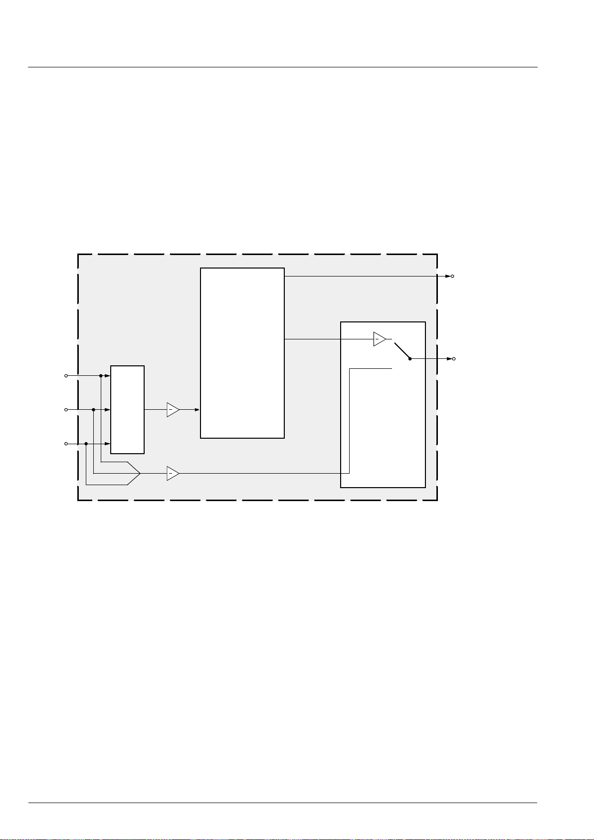
MSP 34x5G PRELIMINARY DATA SHEET
7. Appendix D: Application Information
7.1. Phase Relationship of Analog Outputs
The user does not need to correct output phases when
using the loudspeaker output directly. The SCART1
output has opposite phase.
The following schematics shows the phase relationship of all analog inputs and outputs.
Loudspeaker
SCART1
SCART
SCART2
MONO
DSP
Input
Select
Fig. 7–1: Phase diagram of the MSP 34x5G
Audio
Baseband
Processing
MONO, SCART1...2
SCART1-Ch.
SCART1
SCART
Output Select
92 Micronas
Page 93

PRELIMINARY DATA SHEET MSP 34x5G
7.2. Application Circuit
AHVSS
Signal GND
Tuner
330 nF
330 nF
330 nF
330 nF
330 nF
SIF 1 IN
56 pF 56 pF
MONO_IN
SC1_IN_L
SC1_IN_R
ASG
SC2_IN_L
SC2_IN_R
C s. section 4.6.2.
100
10
µF
-
nF
+
3.3 µF100
18.432
MHz
nF
+
8V (5V)
+
10 µF
100 p 56 p
1kΩ
ANA_IN1+
Alternative circuit for
SIF-input for more
attenuation of video
components:
AGNDC
ANA_IN−
ANA_IN1+
VREFTOP
XTAL_IN
XTAL_OUT
CAPL_M
DACM_L
DACM_R
1 nF
1 nF
1 µF
1 µF
Loudspeaker
5V
5V
DVSS
DVSS
RESETQ
(from Controller, see section 4.6.3.3.)
STANDBYQ
ADR_SEL
I2C_DA
I2C_CL
ADR_WS
ADR_CL
ADR_DA
I2S_WS
I2S_CL
I2S_DA_IN1
I2S_DA_IN2
I2S_DA_OUT
MSP 34x5G
RESETQ
DVSUP
220
pF
470
pF
1.5
nF
10
µF
5 V 5 V 8 V
AVSUP
DVSS
470
pF
1.5
nF
10
µF
AVSS
AVSS
AHVSUP
470
pF
1.5
nF
10
µF
(5 V)
SC1_OUT_L
SC1_OUT_R
D_CTR_I/O_0
D_CTR_I/O_1
AHVSS
VREF1
AHVSS
AHVSS
TESTEN
VREF2
AHVSS
100Ω
100Ω
22 µF
+
22 µF
+
AHVSS
Micronas 93
Page 94

MSP 34x5G PRELIMINARY DATA SHEET
8. Appendix E: MSP 34x5G Version History
MSP 3435G-A2
First release for BTSC-Stereo/SAP and FM-Radio.
MSP 34x5G-B5
– additional package PLQFP64
– digital input specification changed as of version B5
and later (see Section 4.6. on page 53)
– max. analog high supply voltage AHVSUP 8.7 V.
– supply currents changed as of version B5 and later
(see Section 4.6.3. on page 57)
– programmable A2 and carrier mute thresholds
– new D/K standard 0D
: HDEV3 and NICAM
hex
– additional preference in Automatic Standard Detec-
tion
MSP 34x5G-B6
– improved AM-performance (see page 68)
– new D/K standard for Poland
(see Table 3–7 on page 20)
– improved I
2
C hardwa re proble m handling
(see Section 3.1.1. on page 15)
9. Data Sheet History
1. Preliminary data sheet: “MSP 34x5G Multistandard
Sound Processor Family, Edition Oct. 26, 1998, 6251480-1PD. First release of th e p rel im in ary data s hee t .
2. Preliminary data sheet: “MSP 34x5G Multistandard
Sound Processor Family”, Edition July 11, 2000, 6251480-2PD. Second release of the preliminary data
sheet. Major changes:
– section Specifications: specification for PLQFP64
package added
– specification for version B5 and B6 added
(see Appendix E: Version History)
– reset description modified
2
S and ADR functionality added
– I
– MSP 3425G and MSP 3465G added
– Multistandard controller software flow diagram
added
3. Preliminary data sheet: “MSP 34x5G Multistandard
Sound Processor Family”, Jan. 19, 2001, 6251-4803PD. Third release of the preliminary data sheet. Major
changes:
– Section 4.2.: pin allocation for PLQFP64 corrected
2
– I
C-bus description changed
– ACB register: documentation for bit allocation
D_CTR_I/O changed
– faster system-D/K-loop for stereo detection
– extended features in the CONTROL register
(see Section 3.1.2. on page 16)
MSP 34x5G-B8
– fine-tuning of A2-identification and carrier mute
– EIA-J identification: faster transition time stereo/
bilingual to mono
– J17 FM-deemphasis implemented
– input specification for RESETQ and TESTEN
changed
Micronas GmbH
Hans-Bunte-Strasse 19
D-79108 Freiburg (Germany)
P.O. Box 840
D-79008 Freiburg (Germany)
Tel. +49-761-517-0
Fax +49-761-517-2174
E-mail: docservice@micronas.com
Internet: www.micronas.com
Printed in Germany
Order No. 6251-480-3PD
All information and data contained in this data sheet are without any
commitment, are not to be considered as an offer for conclusion of a
contract, nor shall they be construed as to create any liability. Any new
issue of this data sheet invalidates previous issues. Product availability
and delivery are exclusively subject to our respective order confirmation
form; the same applies to orders based on development samples delivered. By this publication, Micronas GmbH does not assume responsibility for patent infr ingements or other right s of third parties whic h may
result from its use.
Further, Micronas GmbH reserves the right to revise this publication
and to make changes to its content, at any time, without obligation to
notify any pe r so n or en tity of such revisions or cha ng es.
No part of this publication may be reproduced, photocopied, stored on a
retrieval system, or transmitted without the express written consent of
Micronas GmbH .
94 Micronas
Page 95

PRELIMINARY DATA SHEET MSP 34X5G
Freigabe-Exemplar
Dec. 11, 2000
6251-480-3PD
Micronas 95
 Loading...