

Page 1
E2O0014-27-X2
¡ Semiconductor MSM81C55-5RS/GS/JS
¡ Semiconductor
This version: Jan. 1998
Previous version: Aug. 1996
MSM81C55-5RS/GS/JS
2048-Bit CMOS STATIC RAM WITH I/O PORTS AND TIMER
GENERAL DESCRIPTION
The MSM81C55-5 has a 2k-bit static RAM (256 bytes) with parallel I/O ports and a timer. It uses
silicon gate CMOS technology and consumes a standby current of 100 micro ampere, maximum,
while the chip is not selected. Featureing a maximum access time of 400 ns, the MSM81C55-5
can be used in an MSM80C85AH system without using wait states. The parallel I/O consists
of two 8-bit ports and one 6-bit port (both general purpose).
The MSM81C55-5 also contains a 14-bit programmable counter/timer which may be used for
sequence-wave generation or terminal count-pulsing.
FEATURES
• High speed and low power achieved with silicon gate CMOS technology
• 256 words x 8bits RAM
• Single power supply, 3 to 6 V
• Completely static operation
• On-chip address latch
• 8-bit programmable I/O ports (port A and B)
• TTL Compatible
• RAM data hold characteristic at 2 V
• 6-bit programmable I/O port (port C)
• 14-bit programmable binary counter/timer
• Multiplexed address/data bus
• Direct interface with MSM80C85AH
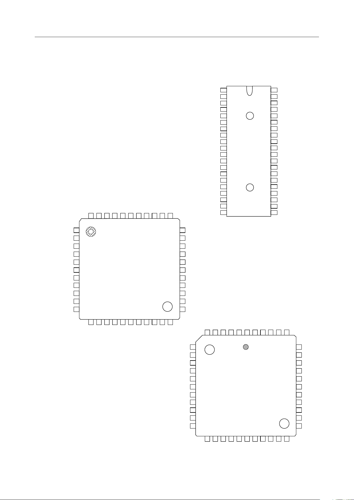
• 40-pin Plastic DIP (DIP40-P-600-2.54): (Product name: MSM81C55-5RS)
• 44-pin Plastic QFJ (QFJ44-P-S650-1.27): (Product name: MSM81C55-5JS)
• 44-pin Plastic QFP (QFP44-P-910-0.80-2K): (Product name: MSM81C55-5GS-2K)
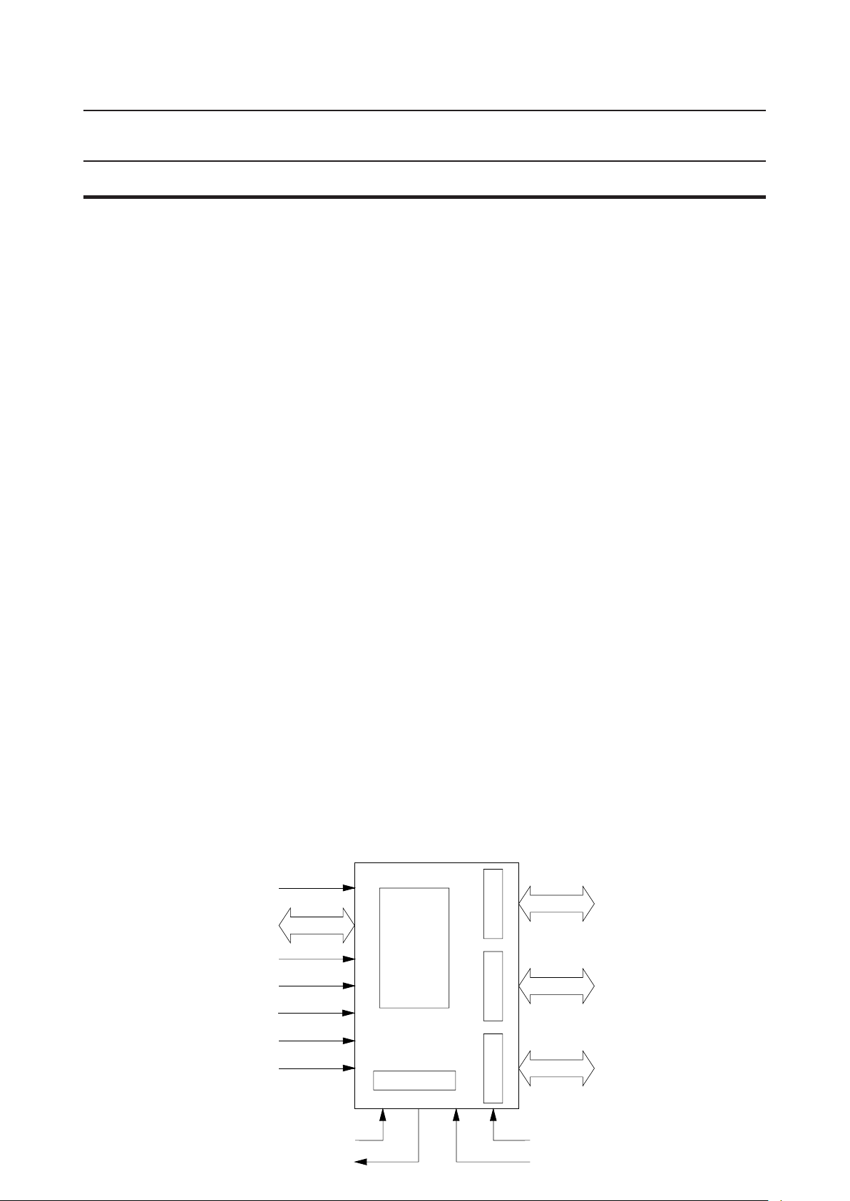
FUNCTIONAL BLOCK DIAGRAM
Port A
8
Port B
8
PA
PB
0 - 7
0 - 7
AD
IO/M
0 - 7
CE
ALE
A
256 ¥ 8
Static
RAM
B
RD
WR
RESET
TIMER IN
TIMER OUT
Timer
Port C
C
6
V
CC
GND (0 V)
(+5 V)
PC
0 - 5
1/19
Page 2
¡ Semiconductor MSM81C55-5RS/GS/JS
PIN CONFIGURATION (TOP VIEW)
40 pin Plastic DIP
TIMEROUT
IO/M
RD
WR
ALE
AD
AD
AD
AD
NC
44 pin Plastic QFP
5
RESET
TIMER IN
PC
PC4PC3V
4443424140
1
2
CE
3
4
5
6
7
0
8
1
9
2
10
3
11 PA
CC
39
2PC1PC0PB7
NC
PC
37
38
363534
1
PC
3
2
PC
4
TIMER IN
TIMER OUT
33
PB
6
PB
32
5
PB
31
4
PB
30
3
PB
29
2
PB
28
1
PB
27
0
26
PA
7
PA
25
6
PA
24
5
23
4
3
4
RESET
5
PC
5
6
7
IO/M
8
CE
9
RD
10
WR
11
ALE
AD
12
0
AD
13
1
AD
14
2
AD
15
3
AD
16
4
AD
17
5
AD
18
6
AD
19
7
20
GND
44 pin Plastic QFJ
40
V
CC
39
PC
2
38
PC
1
37
PC
0
PB
36
7
35
PB
6
34
PB
5
33
PB
4
32
PB
3
31
PB
2
30
PB
1
29
PB
0
28
PA
7
27
PA
6
26
PA
5
25
PA
4
24
PA
3
23
PA
2
22
PA
1
21
PA
0
12131415161718
4AD5
AD
AD6AD7GND
CC
V
192021
0
PA
1PA2PA3
PA
22
NC
TIMER OUT
IO/M
RD
WR
NC
ALE
AD
AD
AD
AD
PC
6
5
RESET
5
TIMER IN
PC4PC3NC
4
3
2
1
2PC1PC0PB7
CC
V
PC
43
44
424140
7
8
CE
9
10
11
12
13
14
0
15
1
16
2
17 PA
3
18192021222324
AD
4
NC
7
AD5AD6AD
GND
252627
0
1PA2PA3PA4
PA
PA
28
39
38
37
36
35
34
33
32
31
30
29
PB
6
PB
5
PB
4
PB
3
PB
2
NC
PB
1
PB
0
PA
7
PA
6
5
2/19
Page 3
¡ Semiconductor MSM81C55-5RS/GS/JS
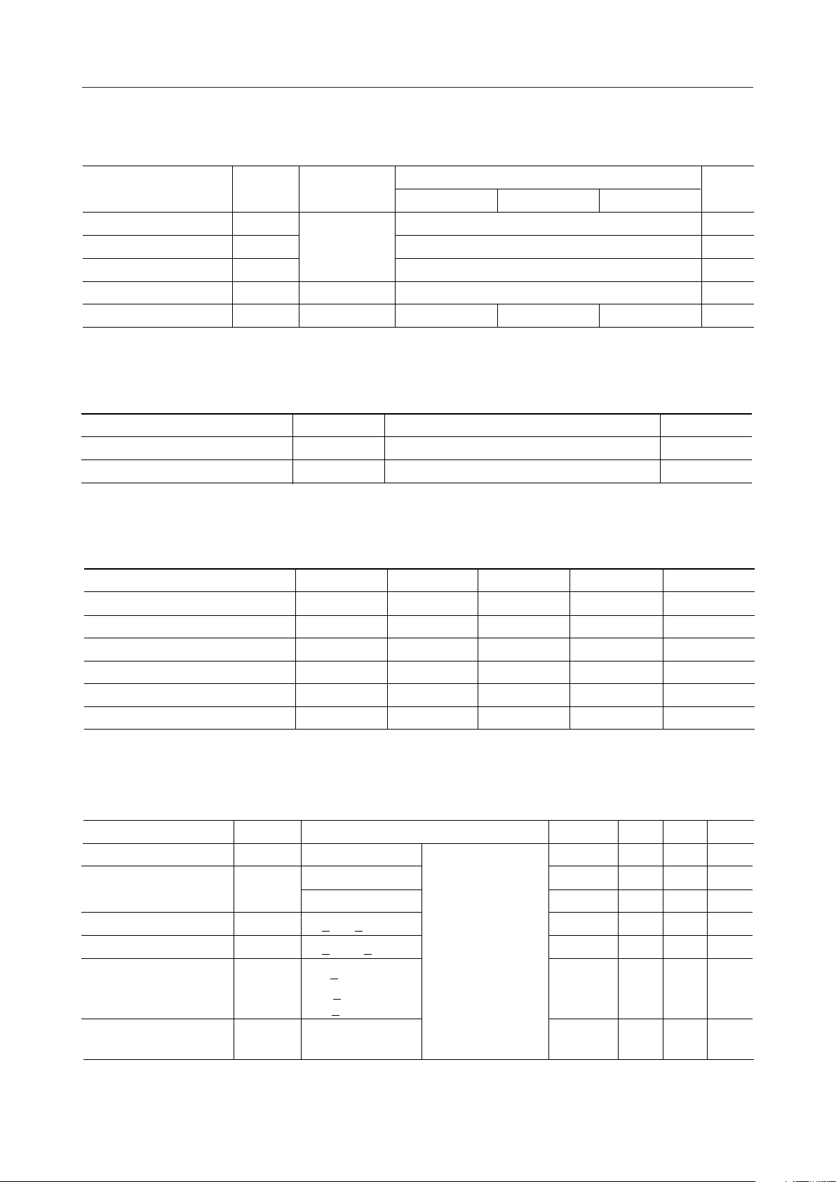
ABSOLUTE MAXIMUM RATING
Parameter Unit
Power Supply Voltage
Input Voltage
Output Voltage
Storage Temperature
Power Dissipation
Symbol
V
CC
V
IN
V
OUT
T
STG
P
D
Conditions
Referenced
to GND
—
Ta = 25°C
MSM81C55-5RS
MSM81C55-5GS MSM81C55-5JS
–0.5 to +7
–0.5 to V
–0.5 to V
CC
CC
+0.5
+0.5
–55 to +150
0.7
1.01.0
OPERATING CONDITION
Rating
Parameter UnitSymbol
Power Supply Voltage
Operating Temperature
V
CC
T
OP
Range
3 to 6
–40 to +85
RECOMMENDED OPERATING CONDITIONS
Parameter UnitSymbol
Power Supply Voltage (81C55)
Operating Temperature (81C55)
"L" Level Input V
"H" Level Input
Supply Voltage (81C55-5)
Operating Temperature (81C55-5)
Min.
V
CC
T
OP
IL
V
IH
V
CC
V
OP
4.5
–40
–0.3
2.2
Typ.
5V
+25
—
—
54.75 5.25
+25–40 +70
Max.
+85
+0.8
V
CC
5.5
+0.3
V
V
V
°C
W
V
°C
°C
V
V
V
°C
DC CHARACTERISTICS
Parameter Unit
"L" Level Output Voltage
"H" Level Output Voltage
Input Leak Current
Output Leak Current
Symbol
V
OL
V
OH
I
LI
I
LO
I
= 2 mA
OL
I
= –400 mA
OH
I
= –40 mA
OH
0 £ V
0 £ V
IN
OUT
CE ≥ V
Standby Current
Mean Operating
Current
I
CCS
I
CC
≥ V
V
IH
V
£ –0.2 V
IL
Memory cycle
time: 1 ms
£ V
CC
CC
£ V
–0.2 V
–0.2 V
Condition
CC
CC
= 4.5 V to 5.5 V
V
CC
= –40°C to 85°C
Ta
Min.
—
2.4
4.2
–10
–10
—
—
Typ. Max.
— 0.45 V
—— V
—— V
—10mA
—10mA
0.1 100 mA
—5mA
3/19
Page 4
¡ Semiconductor MSM81C55-5RS/GS/JS
AC CHARACTERISTICS
V
= 4.75 V to 5.25 V,
CC
Ta = –40 to +70°C
80C85AH 5MHz I/F
Parameter
V
= 4.5 V to 5.5 V,
CC
Symbol Unit Remarks
Ta = –40 to +80°C
80C85AH 3MHz I/F
Min.
Address/latch Setup Time
Latch/address Holt Time
Latch/read (write) Delay Time
Read/output Delay Time
Address/output Delay Time
Latch Width
Read/data Bus Floating Time
Read (write)/latch Delay Time
Read (write) Width
Data In/write Setup Time
Write/data-in Hold Time
Recovery Time
Write/port Output Delay Time
Port Input/read Setup Time Load capaciRead/port Input Hold Time
Strobe/buffer Full Delay Time
Strobe Width
Strobe/buffer Empty Delay Time
Strobe/interrupt-on Delay Time
Read/interrupt-off Delay Time
Port Input/strobe Setup Time
Strobe/port-input Hold Time
Strobe/buffer-empty Delay Time
Write/buffer-full Delay Time
Write/interrupt-off Delay Time
Time Output Delay Time Low
Time Output Delay Time High
Read/data Buse Enable Delay Time
Timer Cycle Time
Timer Input Rise and Fall Times
Timer Input Low Level Time
Timer Input High Level Time
WRITE to TIMER-IN
for writes which start counting
TIMER-IN to WRITE
for writes which start counting
t
t
t
t
RD
t
AD
t
t
RDF
t
t
CC
t
DW
t
WD
t
RV
t
WP
t
PR
t
RP
t
SBF
t
SS
t
RBE
t
t
RDI
t
PSS
t
PHS
t
SBE
t
WBF
t
WI
t
t
TH
t
RDE
t
CYC
tr, t
t
t
t
WT
t
TW
AL
LA
LC
LL
CL
SI
TL
f
1
2
50
30
100
—
—
100
0
20
250
150
0
300
—
70
50
—
200
—
—
—
50
120
—
—
—
—
—
10
320
—
80
120
200
0
Max.
—
—
—
170
400
—
100
—
—
—
—
—
400
—
—
400
—
400
400
400
—
—
400
400
400
400
400
—
—
80
—
—
—
—
37 —
30 —
40 —
— 140
— 330
70 —
080
20 —
200 —
100 —
25 —
200 —
— 300
50 —
10 —
— 300
150 —
— 300
— 300
— 300
20 —
100 —
— 300
— 300
— 300
— 300
— 300
10 —
320 —
—80
40 —
70 —
200 —
0—
Max.Min.
ns
ns
ns
ns
ns
ns
ns
ns
ns
ns
ns
ns
ns
ns
tance: 150 pF
ns
ns
ns
ns
ns
ns
ns
ns
ns
ns
ns
ns
ns
ns
ns
ns
ns
ns
ns
ns
ns
Note: Timings are measured wth VL = 0.8 V and VH = 2.2 V for both input and output.
4/19
Page 5
¡ Semiconductor MSM81C55-5RS/GS/JS
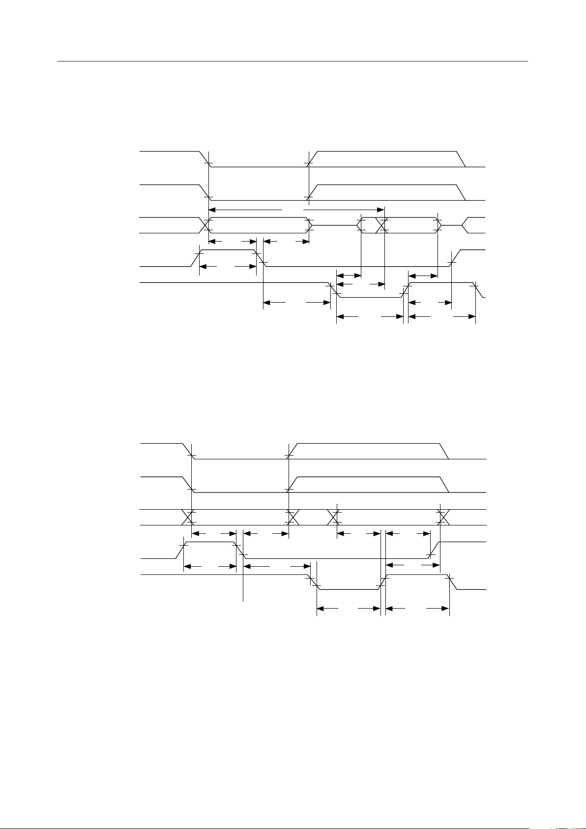
TIMING DIAGRAM
Read Cycle
CE
IO/M
t
AD
t
CC
Data Valid
t
RDF
t
CL
t
RV
AD
0 - 7
ALE
RD
t
LL
t
AL
Address
t
LA
t
RDE
t
RD
t
LC
Write Cycle
IO/M
AD
CE
0 - 7
ALE
WR
t
t
LL
AL
Address
Data Valid
t
LA
t
LC
t
DW
t
CC
t
CL
t
WD
t
RV
5/19
Page 6
¡ Semiconductor MSM81C55-5RS/GS/JS
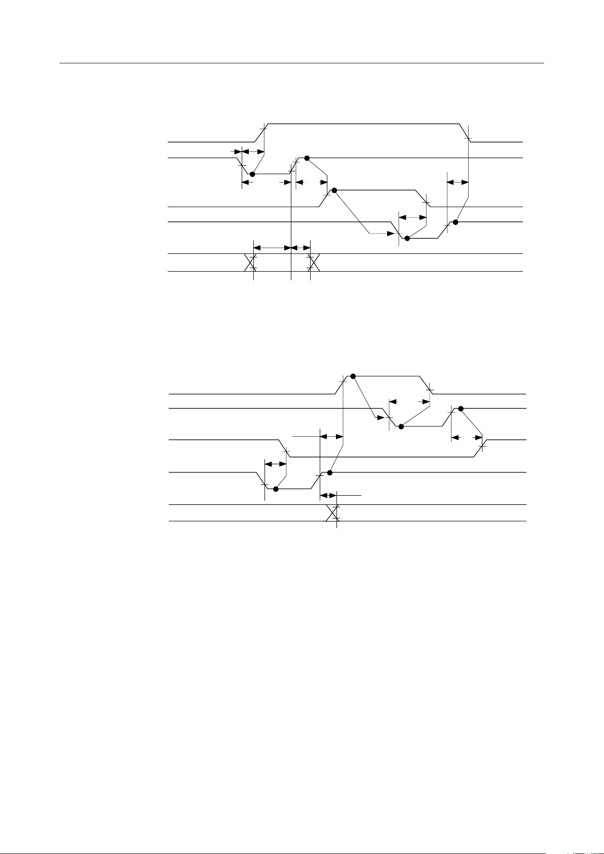
Strobe Input Mode
BF
t
SBF
STROBE
INTR
t
SS
t
SI
t
RDI
t
RBE
RD
Input Data
From Port
Strobe Output Mode
BF
STROBE
INTR
WR
Output Data
To Port
t
PSS
t
WI
t
PHS
t
WBF
t
WP
t
SBE
t
SI
6/19
Page 7

¡ Semiconductor MSM81C55-5RS/GS/JS
y
Basic Input Mode
t
RP
Port Input
Data Bus
Basic Output Mode
Port Output
RD
WR
t
PR
t
WP
Data Bus
Note: The DATA BUS timing is the same as the read and write cycles.
Timer Waveforms 1
Load Counter From
Count Length Register
TIMER IN
TIMER OUT
(Pulse)
TIMER OUT
(Square Wave)
Note: Periodicall
Load Counter From
Count Length Register
t
f
t
t
r
1
t
CYC
t
2
(Note)
t
TL
(Note)
t
TL
Count Down(5Æ1)
outut according to the output mode (m1=1) programming contents.
1234512 5
(T.C)
t
TH
t
TH
7/19
Page 8

¡ Semiconductor MSM81C55-5RS/GS/JS
Timer Waveforms 2
WR
Timer - Start
t
TW
t
WT
TIMER IN
RAM DATA HOLD CHARACTERISTICS AT LOW SUPPLY VOLTAGE
Item UnitSymbol Condition
Data Holding Supply Voltage V
Data Holding Supply Current I
Setup Time t
Hold Time t
CCH
CCH
SU
R
VIN = 0 V or VCC, ALE = 0 V
V
= V
CC
V
= 0 V or V
IN
, ALE = 0
CCH
CC
Specification
Min. Typ.
Max.
2.0 — V
— 0.05 mA
30 — ns
20 —
—
20
—
—ns
Two ways to place device in standby mode:
(1) Method using CE
t
5 V
4.5 V
V
CCH
ALE
0.8 V
0 V
2.2 V
CE
SU
V
CC
t
LA
Standby Mode
t
R
t
AL
V
CCH
8/19
Page 9

¡ Semiconductor MSM81C55-5RS/GS/JS
(2) Method using RESET
V
5 V
CC
4.5 V
2.2 V
V
CCH
GND
Note: In this case, the C/S register is reset, the port is set into the input mode, and the timer stops.
PIN FUNCTION
Symbol Function
RESET
ALE
AD
0 - 7
t
SU
t
R
Standby Mode
RESET
A high level input to this pin resets the chip, places all three I/O ports in the input mode, resets all
output latches and stops timer.
Negative going edge of the ALE (Address Latch Enable) input latches AD
the respective latches.
Three-state, bi-directional address/data bus. Eight-bit address information on this bus is read into
the internal address latch at the negative going edge of the ALE. Eight bits of data can be read from
or written to the chip using this bus depending on the state of the WRITE or READ input.
, IO/M, and CE signals into
0 - 7
CE When the CE input is high, both read and write operations to the chip are disabled.
IO/M A high level input to this pin selects the internal I/O functions, and a low level selects the memory.
RD
WR
PA
(PB
0 - 7
0 - 7
If this pin is low, data from either the memory or ports is read onto the AD
the state of the IO/M line.
If this pin is low, data on lines AD
is written into either the memory or into the selected port
0 - 7
depending on the state of the line IO/M line.
General-purpose I/O pins. Input/output directions can be determined by programming the command/
)
status (C/S) register.
lines depending on
0 - 7
Three pins are usable either as general-purpose I/O pins or control pins for the PA and PB ports.
When used as control pins, they are assigned to the following functions:
PC
: A INTR (port A interrupt)
0
: A BF (port A full)
PC
0 - 5
PC
1
PC
: A STB (port A strobe)
2
PC
: B INTR (port B interrupt)
3
: B BF (port B buffer full)
PC
4
: B STB (port B strobe)
PC
5
TIMER IN Input to the counter/timer
TIMER OUT
V
CC
Timer output. When the present count is reached during timer operation, this pin provides
a square-wave or pulse output depending on the programmed control status.
3–6V power supply
GND GND
9/19
Page 10

¡ Semiconductor MSM81C55-5RS/GS/JS
OPERATION
Description
The MSM81C55-5 has three functions as described below.
• 2K-bit static RAM (256 words ¥ 8 bits)
• Two 8-bit I/O ports (PA and PB) and a 6-bit I/O port (PC)
• 14-bit timer counter
The internal register is shown in the figure below, and the I/O addresses are described in the
table below.
8 Bit Internal Data Bus
A
A
7
¥
¥
¥
¥
¥
¥
6
¥
¥
¥
¥
¥
¥
¥: Don't care.
Command
Status
I/O Address
A
5
¥
¥
¥
¥
¥
¥
PC
6 Bit
A
A
4
¥
¥
¥
¥
¥
¥
A
3
2
¥
¥
¥
¥
¥
¥
0
0
0
0
1
1
PB
8 Bit
A
A
1
0
0
0
1
1
0
0
0
1
0
1
0
1
PA
8 Bit
Internal command/status register
Universal I/O port A (PA)
Universal I/O port B (PB)
I/O port C (PC)
Timer count lower position 8 bits (LSB)
Timer count upper position 6 bits and timer mode
2 bits (MSB)
Timer
MSB
Timer Mode
Selecting Register
Timer
LSB
10/19
Page 11

¡ Semiconductor MSM81C55-5RS/GS/JS
(1) Programming the Command/Status (C/S) Register
The contents of the command register can be written during an I/O cycle by addressing it
with an I/O address of xxxxx000. Bit assignments for the register are shown below:
76543210
TM2 TM1 IEB IEA PC2 PC1 PB PA
Timer Command
Definition of PA
Definition of PB
0 - 7
0 - 7
0= Input
1= Output
00=ALT1
Definition of PC
0 - 5
11=ALT2
01=ALT3
10=ALT4
Port A Interrupt Enable 1 = Enabled
Port B Interrupt Enable 0 = Disabled
00 = NOP : Does not affect counter operations.
01 = STOP : Stops the timer if it is runnning.
NOP if the timer is not runnning.
10 = STOP AFTER TC :
Stops the timer when it reaches TC.
NOP if the timer is not running.
11 = START : If the timer is not running, loads the mode and
the count length, and immediately starts timer operation.
If the timer is running, loads a new mode and the count
length, and starts timer operation immediately after
TC is reached.
See the port
control
assignment
table.
Pin
PC
PC
PC
PC
PC
PC
Port Control Assignment Table
ALT1
0
1
2
3
4
5
Input port
Input port
Input port
Input port
Input port
Input port
ALT2
Output port
Output port
Output port
Output port
Output port
Output port
ALT3
A INTR
A BF
A STB
Output port
Output port
Output port
ALT4
A INTR
A BF
A STB
B INTR
B BF
B STB
11/19
Page 12

¡ Semiconductor MSM81C55-5RS/GS/JS
(2) Reading the C/S Register
The I/O and timer status can be accessed by reading the contents of the Status register
located at I/O address xxxxx000. The status word format is shown below:
AD
7
AD
6
TIMER
AD
INTE
B
AD
5
B
BF
AD
4
INTR
B
AD
3
INTE
A
AD
2
A
BF
AD
1
0
INTR
A
Port A Interrupt Request
Port A Buffer Full
Port A Interrupt Enable
Port B Interrupt Request
Port B Buffer Full
Port B Interrupt Enable
Timer Interrupt. This bit is set high when the timer
reaches TC, and is reset when the C/S register is read
or a hardware reset occurs.
(3) PA and PB Registers
These registers may be used as either input or output ports depending on the programmed
contents of the C/S register. They may also be used either in the basic mode or in the strobe
mode.
I/O address of the PA register: xxxxx001
I/O address of the PB register: xxxxx010
(4) PC Register
The PC register may be used as an input port, output port or control register depending on
the programmed contents of the C/S register. The I/O address of the PC register is
xxxxx011.
(5) Timer
The timer is a 14-bit down counter which counts TIMER IN pulses.
The low order byte of the timer register has an I/O address of xxxxx100, and the high order
byte of the register has an I/O address of xxxxx101.
The count length register (CLR) may be preset with two bytes of data. Bits 0 through 13 are
assigned to the count length and bits 14 and 15 specify the timer output mode. A read
operation of the CLR reads the contents of the counter and the pertinent output mode. The
initial value range which can initially be loaded into the counter is 2 through 3FFF hex. Bit
assignments to the timer counter and possible output modes are shown in the following.
M
Output Mode High Order 6 Bits of Count Length
T
M
2
T
7
T
1
T
6
Low Order Byte of Count Length
13
T
12
T
5
4
T
T
11
T
10
T
3
T
T
2
T
9
1
8
T
0
12/19
Page 13

¡ Semiconductor MSM81C55-5RS/GS/JS
M
M
2
1
0 0 Outputs a low-level signal in the latter half (Note 1) of a count period.
0 1 Outputs a low-level signal in the latter half of a count period, automatically
loads the programmed count length, and restarts counting when the TC
value is reached.
1 0 Outputs a pulse when the TC value is reached.
1 1 Outputs a pulse each time the preset TC value is reached, automatically
loads the programmed count length, and restarts from the beginning.
Notes: 1. When counting an asymmetrical value such as (9), a high level is output during
the first period of five,and a low level is output during the second period of four.
2. If an internal counter of the MSM81C55-5 receives a reset signal, count operation
stops but the counter is not set to a specific initial value or output mode. When
restarting count operation after reset, the START command must be executed
again through the C/S register.
Note that while the counter is counting, you may load a new count and mode into the CLR.
Before the new count and mode will be used by the counter, you must issue a START
command to the counter. Please note the timer circuit on the MSM81C55-5 is designed to
be a square-wave timer, not a event counter. To achieve this, it counts down by twos twice
in completing one cycle. Thus, its registers do not contain values directly representing the
number of TIMER IN pulse received. After the timer has started counting down, the values
residing in the count registers can be used to calculate the actual number of TIMER IN pulse
required to complete the timer cycle if desired. To obtain the remaining count, perform the
following operations in order.
1. STOP the counter
2. Read in the 16-bit value from the count registers.
3. Reset the upper two mode bits
4. Reset the carry and rotate right one position all 16 bits through carry
5. If carry is set, add 1/2 of the full original count (1/2 full count-1 if full count is odd).
Note: If you started with an odd count and you read the count registers before the third
count pulse occurs, you will not be able to recognize whether one or two
counts have occurred. Regardless of this, the MSM81C555 always counts out the right number of pulses in generating the
TIMER OUT waveforms.
TIMER-IN
WR
TIMER-OUT
TIMER-OUT
WR
TIMER-OUT
n=5
(Square Wave)
(Pulse)
n=4
(Square Wave)
Start
Start
55 34 2
(TC)
53 42
(TC)
534
55
TIMER-OUT
Note: n is the value set in the CLR. Figures in the diagram refer to counter values
(Pulse)
13/19
Page 14

¡ Semiconductor MSM81C55-5RS/GS/JS
(6) Standby Mode (see page 7)
The MSM81C55-5 is placed in standby mode when the high level at the CE input is latched
during the negative going edge of ALE. All input ports and the timer input should be pulled
up or down to either VCC or GND potential.
When using battery back-up, all ports should be set low or in input port mode. The timer
output should be set low. Otherwise, a buffer should be added to the timer output and the
battery should be connected to the power supply pins of the buffer.
By setting the reset input to a high level, the standby mode can be selected. In this case, the
command register is reset, so the ports automatically set to the input mode and the timer
stops.
14/19
Page 15

¡ Semiconductor MSM81C55-5RS/GS/JS
NOTICE ON REPLACING LOW-SPEED DEVICES WITH HIGH-SPEED DEVICES
The conventional low speed devices are replaced by high-speed devices as shown below.
When you want to replace your low speed devices with high-speed devices, read the replacement
notice given on the next pages.
High-speed device (New)
M80C85AH
M80C86A-10
M80C88A-10
M82C84A-2
M81C55-5
M82C37B-5
M82C51A-2
M82C53-2
M82C55A-2
Low-speed device (Old)
M80C85A/M80C85A-2
M80C86A/M80C86A-2
M80C88A/M80C88A-2
M82C84A/M82C84A-5
M81C55
M82C37A/M82C37A-5
M82C51A
M82C53-5
M82C55A-5
Remarks
8bit MPU
16bit MPU
8bit MPU
Clock generator
RAM.I/O, timer
DMA controller
USART
Timer
PPI
15/19
Page 16

¡ Semiconductor MSM81C55-5RS/GS/JS
Differences between MSM81C55-5 and MSM81C55
1) Manufacturing Process
These devices use a 3 m Si-CMOS.
2) Design
These devices use the same chip. However, different outgoing inspection standards are used for
these devices separately.
3) Electrical Characteristics
''Oki's '96 Data Book for MICROCONTROLLER'' describes that the MSM81C55-5 satisfies the
electrical characteristics of the MSM81C55.
As shown above, the devices can be replaced without any trouble.
16/19
Page 17

¡ Semiconductor MSM81C55-5RS/GS/JS
PACKAGE DIMENSIONS
(Unit : mm)
DIP40-P-600-2.54
Package material
Lead frame material
Pin treatment
Solder plate thickness
Package weight (g)
Epoxy resin
42 alloy
Solder plating
5 mm or more
6.10 TYP.
Notes for Mounting the Surface Mount Type Package
The SOP, QFP, TSOP, SOJ, QFJ (PLCC), SHP and BGA are surface mount type packages, which
are very susceptible to heat in reflow mounting and humidity absorbed in storage.
Therefore, before you perform reflow mounting, contact Oki’s responsible sales person for the
product name, package name, pin number, package code and desired mounting conditions
(reflow method, temperature and times).
17/19
Page 18

¡ Semiconductor MSM81C55-5RS/GS/JS
(Unit : mm)
QFJ44-P-S650-1.27
Mirror finish
Package material
Lead frame material
Pin treatment
Solder plate thickness
Package weight (g)
Epoxy resin
Cu alloy
Solder plating
5 mm or more
2.00 TYP.
Notes for Mounting the Surface Mount Type Package
The SOP, QFP, TSOP, SOJ, QFJ (PLCC), SHP and BGA are surface mount type packages, which
are very susceptible to heat in reflow mounting and humidity absorbed in storage.
Therefore, before you perform reflow mounting, contact Oki’s responsible sales person for the
product name, package name, pin number, package code and desired mounting conditions
(reflow method, temperature and times).
18/19
Page 19

¡ Semiconductor MSM81C55-5RS/GS/JS
(Unit : mm)
QFP44-P-910-0.80-2K
Mirror finish
Package material
Lead frame material
Pin treatment
Solder plate thickness
Package weight (g)
Epoxy resin
42 alloy
Solder plating
5 mm or more
0.41 TYP.
Notes for Mounting the Surface Mount Type Package
The SOP, QFP, TSOP, SOJ, QFJ (PLCC), SHP and BGA are surface mount type packages, which
are very susceptible to heat in reflow mounting and humidity absorbed in storage.
Therefore, before you perform reflow mounting, contact Oki’s responsible sales person for the
product name, package name, pin number, package code and desired mounting conditions
(reflow method, temperature and times).
19/19
 Loading...