

Page 1

E2O0009-27-X2
¡ Semiconductor MSM80C85AHRS/GS/JS
¡ Semiconductor
This version: Jan. 1998
Previous version: Aug. 1996
MSM80C85AHRS/GS/JS
8-Bit CMOS MICROPROCESSOR
GENRAL DESCRIPTION
The MSM80C85AH is a complete 8-bit parallel; central processor implemented in silicon gate
C-MOS technology and compatible with MSM80C85A.
It is designed with higher processing speed (max.5 MHz) and lower power consumption
compared with MSM80C85A and power down mode is provided, thereby offering a high level
of system integration.
The MSM80C85AH uses a multiplexed address/data bus. The address is split between the 8bit address bus and the 8-bit data bus. The on-chip address latch : of a MSM81C55-5 memory
product allows a direct interface with the MSM80C85AH.
FEATURES
• Power down mode (HALT-HOLD)
• Low Power Dissipation: 50mW(Typ)
• Single + 3 to + 6 V Power Supply
• –40 to + 85°C, Operating Temperature
• Compatible with MSM80C85A
• 0.8 ms instruction Cycle (VCC = 5V)
• On-Chip Clock Generator (with External Crystal)
• On-Chip System Controller; Advanced Cycle Status Information Available for Large System
Control
• Bug operation in MSM80C85AH is fixed
• Four Vectored interrupt (One is non-maskable) Plus the 8080A-compatible interrupt.
• Serial, In/Serial Out Port
• Decimal, Binary and Double Precision Arithmetic
• Addressing Capability to 64K Bytes of Memory
• TTL Compatible
• 40-pin Plastic DIP(DIP40-P-600-2.54): (Product name: MSM80C85AHRS)
• 44-pin Plastic QFJ(QFJ44-P-S650-1.27): (Product name: MSM80C85AHJS)
• 44-pin Plastic QFP(QFP44-P-910-0.80-2K): (Product name: MSM80C85AHGS-2K)
1/29
Page 2
¡ Semiconductor MSM80C85AHRS/GS/JS
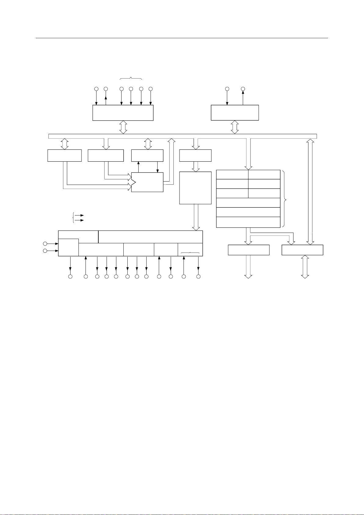
FUNCTIONAL BLOCK DIAGRAM
RST
INTR INTA 5.5 6.5 7.5 TRAP SID SOD
Interrupt Control Serial I/O Control
8-Bit Internal Data Bus
Accumulator
(8)
Power
Supply
Power Down
X
1
X
2
CLK
GEN
CLK
OUT
Temporary Register
(8)
+5V
GND
Control Status DMA Reset
READY RD WR ALE S0 S1 IO / M HOLD HLDA RESET IN RESET OUT
Flag (5)
Flip Flops
Arithmetic
Logic Unit
ALU(8)
Timing And Control
Instruction
Register (8)
Instruction
Decoder
And
Machine
Cycle
Encoding
B REG (8)
D REG (8)
H REG (8)
Stack Pointer (16)
Program Counter (16)
Incrementer/Decrementer
Address Latch (16)
Address Buffer (8)
Address Bus
C REG (8)
E REG (8)
C REG (8)
A
- A
15
8
Register
Array
Data/Address
Buffer (8)
AD
- AD
7
Address/Data Bus
0
2/29
Page 3
¡ Semiconductor MSM80C85AHRS/GS/JS
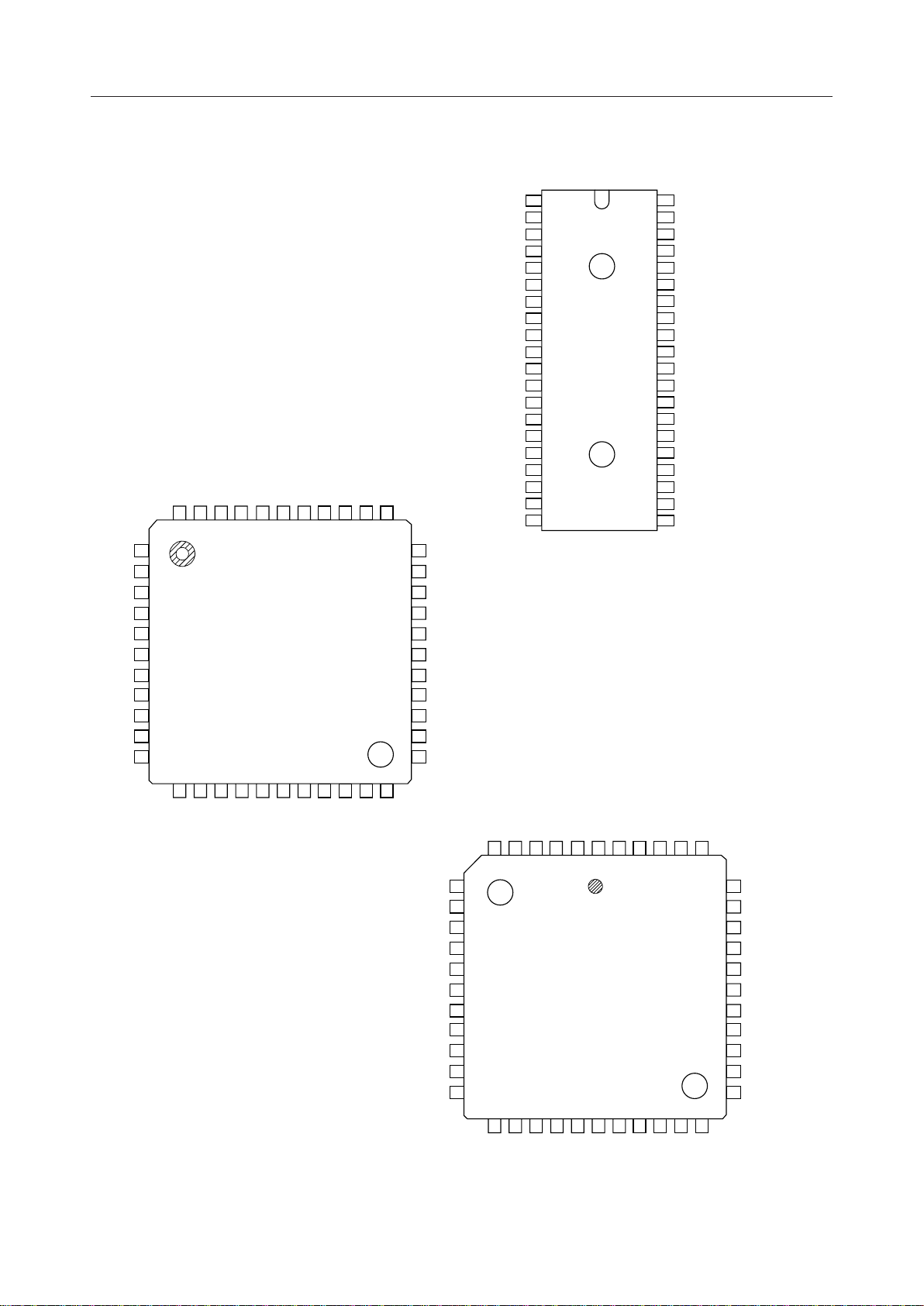
PIN CONFIGURATION (TOP VIEW)
40 pin Plastic DIP
44 pin Plastic QFP
SOD
2X1
RESET OUT
X
SID
4443424140
TRAP
1
RST7.5
2
RST6.5
3
RST5.5
4
INTR
5
INTA
6
AD
7
0
8
AD
1
9
AD
2
10
AD
3
NC
11 A
NC
39
CC
V
HOLD
37
38
HLDA
CLK(OUT)
363534
RESET IN
33
32
31
30
29
28
27
26
25
24
23
READY
IO/M
S
1
RD
WR
ALE
S
0
A
15
A
14
A
13
12
RESET OUT
SOD
SID
TRAP
RST7.5
RST6.5
RST5.5
INTR
INTA
AD
AD
AD
AD
AD
AD
AD
AD
GND
1
X
1
2
X
2
3
4
5
6
7
8
9
10
11
12
0
13
1
14
2
15
3
16
4
17
5
18
6
19
7
20
44 pin Plastic QFJ
40
39
38
37
36
35
34
33
32
31
30
29
28
27
26
25
24
23
22
21
V
CC
HOLD
HLDA
CLK(OUT)
RESET IN
READY
IO/M
S
1
RD
WR
ALE
S
0
A
15
A
14
A
13
A
12
A
11
A
10
A
9
A
8
12131415161718
4AD5AD6AD7
AD
GND
CC
V
192021
8
A
A10A
22
11
NC
SID
SOD
RESET OUT
X2X1NC
6
5
4
3
7
TRAP
RST7.5
8
RST6.5
9
RST5.5
10
INTR
11
NC
12
INTA
13
14
AD
0
15
AD
1
16
AD
2
AD
17 A
3
18192021222324
4
5AD6AD7
NC
AD
AD
CC
V
HOLD
HLDA
CLK(OUT)
RESET IN
2
1
43
44
424140
39
READY
38
IO/M
37
S
1
RD
36
WR
35
NC
34
ALE
33
32
S
0
A
31
15
A
30
14
29
13
25
262728
8
GND
9
A
A
A10A11A
12
9
A
3/29
Page 4

¡ Semiconductor MSM80C85AHRS/GS/JS
MSM80C85AH FUNCTIONAL PIN DEFINITION
The following describes the function of each pin:
Symbol Function
- A
A
8
15
(Output, 3-state)
A0 - A
7
(Input/Output)
3-state
ALE
(Output)
, S1 , IO/M
S
0
(Output)
RD
(Output, 3-state)
WR
(Output, 3-state)
READY
(Input)
HOLD
(Input)
HLDA
(Output)
INTR
(Output)
INTA
(Output)
RST 5.5
RST 6.5
RST 7.5
(Input)
TRAP
(Input)
Address Bus: The most significant 8-bits of the memory address or the 8-bits of the I/O address,
3-stated during Hold and Halt modes and during RESET.
Multiplexed Address/Data Bus: Lower 8-bits of the memory address (or I/O address) appear on
the bus during the first clock cycle (T state) of a machine cycle. It then becomes the data bus during
the second and third clock cycles.
Address Latch Enable: It occurs during the first clock state of a machine cycle and enables address to
get latched into the on-chip latch peripherals. The falling edge of ALE is set to guarantee setup and
hold times for the address information. The falling edge ALE can also be used to strobe the status
information ALE is never 3-state.
Machine cycle status:
S0 States
IO/M S
1
Memory write
1
0
0
Memory read
0
1
0
I/O write
1
0
1
I/O read
0
1
1
Opcode fetch
1
1
0
S
can be used as an advanced R/W status. IO/M, S
1
IO/M S
S0 States
1
Interrupt Acknowledge
1
1
1
Halt = 3-state
0
0
.
Hold (high impedance)
¥
¥
.
Reset ¥ = unspecified
¥
¥
.
and S1 become valid at the beginning of
0
a machine cycle and remain stable throughout the cycle. The falling edge of ALE may be used to latch
the state of these lines.
READ control: A low level on RD indicates the selected memory or I/O device is to be read that
the Data Bus is available for the data transfer, 3-stated during Hold and Halt modes and during RESET.
WRITE control: A low level on WR indicates the data on the Data Bus is to be written into the selected
memory or I/O location. Data is set up at the trailing edge of WR, 3-stated during Hold and Halt
modes and during RESET.
If READY is high during a read or write cycle, it indicates that the memory or peripheral is ready to
send or receive data. If READY is low, the cpu will wait an integral number of clock cycles for READY
to go high before completing the read or write cycle READY must conform to specified setup and
hold times.
HOLD indicates that another master is requesting the use of the address and data buses.
The cpu, upon receiving the hold request, will relinquish the use of the bus as soon as the completion
of the current bus transfer. Internal processing can continue. The processor can regain the bus only
after the HOLD is removed. When the HOLD is acknowledged, the Address, Data, RD, WR, and IO/M
lines are 3-stated. And status of power down is controlled by HOLD.
HOLD ACKNOWLEDGE: Indicates that the cpu has received the HOLD request and that it will
relinquish the bus in the next clock cycle. HLDA goes low after the Hold request is removed.
The cpu takes the bus one half clock cycle after HLDA goes low.
INTERRUPT REQUEST: Is used as a general purpose interrupt. It is sampled on during the next to
the last clock cycle of an instruction and during Hold and Halt states. If it is active, the Program
Counter (PC) will be inhibited from incrementing and an INTA will be issued. During this cycle
a RESTART or CALL instruction can be inserted to jump to the interrupt service routine.
The INTR is enabled and disabled by software. It is disabled by Reset and immediately after
an interrupt is accepted. Power down mode is reset by INTR.
INTERRUPT ACKNOWLEDGE: Is used instead of (and has the same timing as) RD during
the instruction cycle after an INTR is accepted.
RESTART INTERRUPTS: These three inputs have the same timing as INTR except they cause
an internal RESTART to be automatically inserted.
The priority of these interrupts is ordered as shown in Table 1. These interrupts have a higher priority
than INTR. In addition, they may be individually masked out using the SIM instruction.
Power down mode is reset by these interrupts.
Trap interrupt is a nonmaskable RESTART interrupt. It is recognized at the same timing as INTR or
RST 5.5 - 7.5. It is unaffected by any mask or Interrupt Disable. It has the highest priority of any
interrupt. (See Table 1.) Power down mode is reset by input of TRAP.
4/29
Page 5
¡ Semiconductor MSM80C85AHRS/GS/JS
Symbol Function
Sets the Program Counter to zero and resets the Interrupt Enable and HLDA flip-flops and release
power down mode. The data and address buses and the control lines are 3-stated during RESET and
RESET IN
(Input)
RESET OUT
(Output)
, X
X
1
2
(Input)
CLK
(Output)
SID
(Input)
SOD
(Output)
V
CC
GND Ground Reference.
because of the asynchronous nature of RESET IN, the processor's internal registers and flags may be
altered by RESET with unpredictable results. RESET IN is a Schmitt-triggered input, allowing
connection to an R-C network for power-on RESET delay. The cpu is held in the reset condition as
long as RESET IN is applied.
Indicated cpu is being reset. Can be used as a system reset. The signal is synchronized to
the processor clock and lasts an integral number of clock periods.
and X2 are connected to a crystal to drive the internal clock generator. X1 can also be an external
X
1
clock input from a logic gate. The input frequency is divided by 2 to give the processor's internal
operating frequency.
Clock Output for use as a system clock. The period of CLK is twice the X1, X2 input period.
Serial input data line. The data on this line is loaded into accumulator bit 7 whenever a RIM instruction
is executed.
Serial output data line. The output SOD is set or reset as specified by the SIM instruction.
+ 5 Volt supply
Name
TRAP
RST 7.5
RST 6.5
RST 5.5
INTR
Table 1 Interrupt Priority, Restart Address, and Sensitivity
Priority
Address Branched To (1)
When Interrupt Occurs
1 24H
2
3
4
5
3CH
34H
2CH
(2)
Rising edge and high level unit sampled.
Rising edge (latched).
High level unitl sampled.
High level until sampled.
High level until sampled.
Type Trigger
Notes: (1) The processor pushes the PC on the stack before branching to the indicated
address.
(2) The address branched to depends on the instruction provided to the cpu
when the interrupt is acknowledged.
5/29
Page 6
¡ Semiconductor MSM80C85AHRS/GS/JS
FUNCTIONAL DESCRIPTION
The MSM80C85AH is a complete 8-bit parallel central processor. It is designed with silicon gate
C-MOS technology and requires a single +5 volt supply. Its basic clock speed is 5 MHz, thus
improving on the present MSM80C85A's performance with higher system speed and power
down mode. Also it is designed to fit into a minimum system of two IC's: The CPU
(MSM80C85AH), and a RAM/IO (MSM81C55-5)
The MSM80C85AH has twelve addressable 8-bit register pairs. Six others can be used
interchangeably as 8-bit registers or 16-bit register pairs. The MSM80C85AH register set is as
follows:
Mnemonic
ACC or A
PC
BC, DE, HL
SP
Flags or F
Register
Accumulator
Program Counter
General-Purpose Registers; data pointer (HL)
Stack Pointer
Flag Register
8-bits
16-bit address
8-bit ¥ 6 or 16-bits ¥ 3
16-bit address
5 flags (8-bit space)
Contents
The MSM80C85AH uses a multiplexed Data Bus. The address is spilt between the higher 8-bit
Address Bus and the lower 8-bit Address/Data Bus. During the first T state (clock cycle) of a
machine cycle the low order address is sent out on the Address/Data Bus. These lower 8-bits
may be latched externally by the Address Latch Enable signal (ALE). During the rest of the
machine cycle the data bus is used for mamory or I/O data.
The MSM80C85AH provides RD, WR, S0, S1, and IO/M signals for bus control. An Interrupt
Acknowledge signal (INTA) is also provided. Hold and all Interrupts are synchronized with
the processor's internal clock. The MSM80C85AH also provides Serial Input Data (SID) and
Serial Output Data (SOD) lines for a simple serial interface.
In addition to these features, the MSM80C85AH has three maskable, vector interrupt pins, one
nonmaskable TRAP interrupt and power down mode with HALT and HOLD.
INTERRUPT AND SERIAL I/O
The MSM80C85AH has 5 interrupt inputs: INTR, RST 5.5 RST 6.5, RST 7.5, and TRAP. INTR is
identical in function to the 8080A INT. Each of the three RESTART inputs, 5.5, 6.5, and 7.5, has
a programmable mask. TRAP is also a RESTART interrupt but it is nonmaskable.
The three maskable interrupts cause the internal execution of RESTART ( saving the program
counter in the stack branching to the RESTART address) it the interrupts are enable and if the
interrupt mask is not set. The nonmaskable TRAP causes the internal execution of a RESTART
vector independent of the state of the interrupt enable or masks. (See Table 1.)
There are two different types of inputs in the restart interrupt. RST 5.5 and RST 6.5 are high
level-sensitive like INTR (and INT on the 8080A) and are recognized with the same timing as
INTR. RST 7.5 is rising edge-sensitive.
6/29
Page 7
¡ Semiconductor MSM80C85AHRS/GS/JS
g
For RST 7.5, only a pulse is required to set an internal flip-flop which generates the internal
interrupt request. The RST 7.5 request flip-flop remains set until the request is serviced. Then
it is reset automatically, This flip-flop may also be reset by using the SIM instruction or by
issuing a RESET␣ IN to the MSM80C85AH. The RST 7.5 internal flip-flop will be set by a pulse
on the RST 7.5 pin even when the RST 7.5 interrupt is masked out.
The interrupts are arranged in a flixed priority that determines which interrupt is to be
recognized if more than one is pending, as follows: TRAP-highest priority, RST 7.5, RST 6.5, RST
5.5, INTR-lowest priority. This priority scheme does not take into account the priority of a
routine that was started by a higher priority interrupt. RST 5.5 can interrupt an RST 7.5 routine
if the interrupt are re-enabled before the end of the RST 7.5 routine.
The TRAP interrupt is useful for catastrophic evens such as power failure or bus error. The
TRAP input is recognized just as any other interrupt but has the highest priority. It is not
affected by any flag or mask. The TRAP input is both edge and level sensitive. The TRAP input
must go high and remain high until it is acknowledged. It will not be recognized again until it
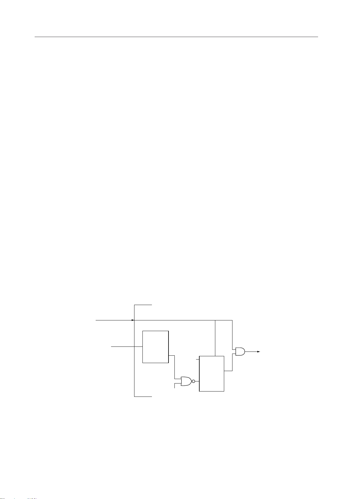
goes low, then high again. This avoids any false triggering due to noise or logic glitches. Figure
3 illustrates the TRAP interrupt request circuitry within the MSM80C85AH. Note that the
servicing of any interrupt (TRAP, RST 7.5, RST 6.5, RST 5.5,INTR) disables all future interrupts
(except TRAPs) until an El instruction is executed.
The TRAP interrupt is special in that it disables interrupts, but preserves the previous interrupt
enable status. Performing the first RIM instruction following a TRAP interrupt allows you to
determine whether interrupts were enabled or disabled prior to the TRAP. All subsequent RIM
instructions provide current interrupt enable status. Performing a RIM instruction following
INTR or RST 5.5-7.5 will provide current interrupt Enable status, revealing that Interrupts are
disabled.
The serial I/O system is also controlled by the RIM and SIM instructions. SID is read by RIM,
and SIM sets the SOD data.
External TRAP
Interrupt Request
RESET IN
Inside the MSM80C85AH
TRAP
RESET
Schmitt
Trigger
Internal
TRAP
Acknowledge
+5 V
CLK
D
D
F/F
Clear
TRAP F.F
TRAP
Interrupt
Q
Request
ure 3 Trap and RESET IN Circuit
Fi
7/29
Page 8
¡ Semiconductor MSM80C85AHRS/GS/JS
p
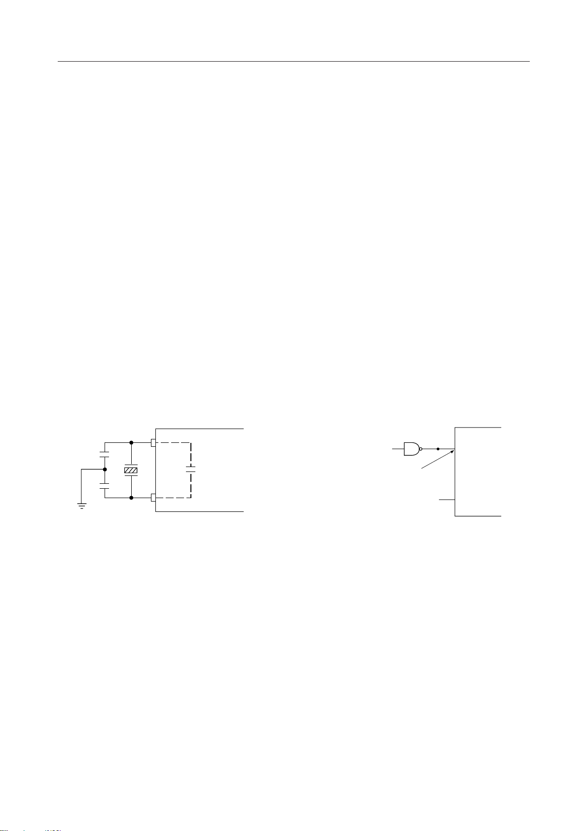
DRIVING THE X1 AND X2 INPUTS
You may drive the clock inputs of the MSM80C85AH with a crystal, or an external clock source.
The driving frequency must be at least 1 MHz, and must be twice the desired internal clock
frequency; hence, the MSM80C85AH is operated with a 6 MHz crystal (for 3 MHz clock). If a
crystal is used, it must have the following characteristics:
Parallel resonance at twice the clock frequency desired
CL (load capacitance) £ 30 pF
CS (shunt capacitance) £ 7 pF
RS (equivalent shunt resistance) £ 75 ohms
Drive level: 10 mW
Frequency tolerance: ± 0.05% (suggested)
Note the use of the capacitors between X1, X2 and ground. These capacitors are required to
assure oscillator startup at the correct frequency.
Figure 4 shows the recommended clock driver circuits. Note in B that a pull-up resistor is
required to assure that the high level voltage of the input is at least 4 V.
For driving frequencies up to and including 6 MHz you may supply the driving signal to X, and
leave X2 open-circuited (Figure 4B). To prevent self-oscillation of the MSM80C85AH, be sure
that X2 is not coupled back to X1 through the driving circuit.
A. Quartz Crystal Clock Driver
1
2
MSM80C85AH
C
= 15 pF
INT
X
C
1
C
2
X
33 pF Capacitor required for crystal frequency 10 to 6.25 MHz
50 pF Capacitor required for crystal frequency 6.25 to 4 MHz
100
F Capacitor required for crystal frequency <4 MHz
B. 1 - 10 MHz Input Frequency External
Clock Drive Circuit
X
1
VIH > 0.8 V
High time > 40 ns
Low time > 40 ns
CC
* X
*
Left Floating
2
X
2
Note: Since the constant values may vary depending on oscillator, consult the manufacturer
of the oscillator used when designing a circuit.
Figure 4 Clock Driver Circuits
8/29
Page 9
¡ Semiconductor MSM80C85AHRS/GS/JS
BASIC SYSTEM TIMING
The MSM80C85AH has a multiplexed Data Bus. ALE is used as a strobe to sample the lower
8-bits of address on the Data Bus. Figure 5 shows an instruction fetch, memory read and I/O
write cycle (as would occur during processing of the OUT instruction). Note that during the I/
O write and read cycle that the I/O port address is copied on both the upper and lower half of
the address.
There are seven possible types of machine cycles. Which of these seven takes place is defined
by the status of the three status lines (IO/M, S1, S0) and the three control signals (RD, WR,and
INTA). (See Table 2.) The status line can be used as advanced controls (for device selection, for
example), since they become active at the T1 state, at the outset of each machine cycle. Control
lines RD and WR become active later, at the time when the transfer of data is to take place, so
are used as command lines.
A machine cycle normally consists of three T states, with the exception of OPCODE FETCH,
which normally has either four or six T states (unless WAIT or HOLD states are forced by the
receipt of READY or HOLD inputs). Any T state must be one of ten possible states, shown in
Table 3.
Machine Cycle
Opcode Fetch
Memory Read
Memory Write
I/O Read
I/O Write
Acknowledge of INTR
Bus Idle
Table 2 MSM80C85AH Machine Cycle Chart
Status Control
(OF)
(MR)
(MW)
(IOR)
(IOW)
(INA)
(BI): DAD
ACK. OF
RST, TRAP
HALT
IO/M S
0
O
O
1
1
1
0
1
TS
1
1
1
0
1
0
1
1
1
0
S
0
1
O
1
O
1
1
0
1
0
RD WR INTA
0
O
1
O
1
1
1
1
TS
1
1
0
1
0
1
1
1
TS
1
1
1
1
1
0
1
1
1
9/29
Page 10

¡ Semiconductor MSM80C85AHRS/GS/JS
Table 3 MSM80C85AH Machine State Chart
Machine State
Status & Buses Control
A
T
1
T
2
T
WAIT
T
3
T
4
T
5
T
6
T
RESET
T
HALT
T
HOLD
S1, S
¥
¥
¥
¥
1
1
1
¥
0
¥
0
IO/M
¥
¥
¥
¥
(2)
0
(2)
0
(2)
0
TS
TS
TS
– A
8
TS
TS
TS
¥
¥
¥
¥
¥
¥
¥
15
AD0 – AD
¥
¥
¥
¥
TS
TS
TS
TS
TS
TS
7
RD, WR
1
¥
¥
¥
1
1
1
TS
TS
TS
0 = Logic "0"
1 = Logic "1"
TS = High Impedance
¥ = Unspecified
Notes: (1) ALE not generated during 2nd and 3rd machine cycles of DAD instruction.
(2) IO/M = 1 during T
- T6 of INA machine cycle.
4
INTA ALE
1
¥
¥
¥
1
1
1
1
1
1
1
0
0
0
0
0
0
0
0
0
(1)
CLK
A
8-15
AD
0-7
ALE
RD
WR
IO/M
STATUS
M
1
T
1
T
2
T
3
T
4
T
1
PCH (High Order Address) (PC+1)H
PC
L
(Low Order
Address)
Data from Memory
(Instruction)
(PC+1)
L1
S1S0(Fetch) 10 (Read) 01 Write 11
Figure 5 MSM80C85AH Basic System Timing
M
2
T
2
Data from Memory
(I/O Port Address)
T
M
3
3
T
1
T
2
T
3
T
IO Port
IO Port
Data to Memory
or Peripheral
10/29
Page 11

¡ Semiconductor MSM80C85AHRS/GS/JS
POWER DOWN Mode
The MSM80C85AH is compatible with the MSM80C85A in function and POWER DOWN mode.
This reduces power consumption further.
There are two methods available for starting this POWER DOWN mode. One is through
software control by using the HALT command and the other is under hardware control by using
the pin HOLD. This mode is released by the HOLD, RESET, and interrupt pins (TRAP, RST7.5,
RST6.5 RST5.5, or INTR). (See Table 4.)
Since the sequence of HALT, HOLD, RESET, and INTERRUPT is compatible with MSM80C85A,
every the POWER DOWN mode can be used with no special attention.
Table 4 POWER DOWN Mode Releasing Method
Start by means of Halt command
Start by means of HOLD pin
Released by using pins RESET and INTERRUPT (not by pin HOLD)
Released by using RESET and HOLD pins (not by interrupt pins)
(1) Start by means of HALT command (See Figures 6 and 7.)
The POWER DOWN mode can be started by executing the HALT command.
At this time, the system is put into the HOLD status and therefore the POWER DOWN mode
cannot be released even when the HOLD is released later.
In this case, the POWER DOWN mode can be released by means of the RESET or interrupt.
(2) Start by means of HOLD pin (See Figure 8.)
During the execution of commands other than the HALT, the POWER DOWN mode is started
when the system is put into HOLD status by means of the HOLD pin.
Since no interrupt works during the execution of the HOLD, the POWER DOWN mode cannot
be released by means of interrupt pins. In this case, the POWER DOWN mode can be released
either by means of the RESET pin or by releasing the HOLD status by means of HOLD pin.
11/29
Page 12

¡ Semiconductor MSM80C85AHRS/GS/JS
CLK (OUT)
ALE
AD
CPU MODE
RESET IN
M
1
T
T
1
Address
0-7
T
2
3
76H
Run Run
M
2
T
T
4
1
Address Address
T
Power Down
HLT
T
RESET
M
1
T
T
1
2
Figure 6 Started by HALT and Released by RESET IN
M
1
T
T
1
T
2
3
M
2
T
T
4
1
T
HLT
M
1
T
T
1
2
CLK (OUT)
ALE
RST5.5
CPU MODE
CLK (OUT)
ALE
Run Run
Power Down
Figure 7 Started by HALT and Released by RST5.5
M
1
T
T
T
1
2
T
3
4
T
HOLD
M
1
T
T
1
2
HOLD
HLDA
CPU MODE
Run RUN
Power Down
Figure 8 Started and Released by HOLD
12/29
Page 13

¡ Semiconductor MSM80C85AHRS/GS/JS
ABSOLUTE MAXIMUM RATINGS
Parameter Units
Power Supply Voltage
Input Voltage
Output Voltage
Storage Temperature
Power Dissipation
Symbol
V
CC
V
IN
V
OUT
T
STG
P
D
Condition
With respect
to GND
—
Ta = 25°C
MSM80C85AHRS
MSM80C85AHGS MSM80C85AHJS
–0.5 - 7
–0.5 - V
–0.5 - V
CC
CC
+
+
0.5
0.5
–55 - +150
0.7
1.01.0
OPERATING RANGE
Limits
Parameter UnitSymbol
Power Supply Voltage
Operating Temperature
V
CC
T
OP
Limits
3 - 6
–40 - +85
RECOMMENDED OPERATING CONDITIONS
Parameter UnitSymbol
Power Supply Voltage
Operating Temperature
"L" Input Voltage V
"H" Output Voltage
RESET IN
"L"
Input Voltage
RESET IN
"H"
Input Voltage
V
V
Min.
V
CC
T
OP
IL
V
IH
ILR
IHR
4.5
–40
–0.3
2.2
Typ.
5V
+25
—
—
—–0.3 +0.8
—3.0 V
Max.
+85
+0.8
V
CC
CC
5.5
+0.3
+0.3
V
V
V
°C
W
V
°C
°C
V
V
V
V
DC CHARACTERISTICS
Parameter Unit
"L" Output Voltage
"H" Output Voltage V
Input Leak Current
Output Leak Current
Operating Supply
Current
Symbol
V
OL
OH
I
LI
I
LO
I
CC
I
= 2.5 mA
OL
I
= –2.5 mA
OH
I
= –100 mA
OH
0 £ V
0 £ V
T
C
T
C
£ V
IN
CC
£ V
OUT
= 200 ns
cyc
= 0 pF at reset
L
= 200 ns
cyc
= 0 pF at power
L
down mode
Conditions
V
CC
CC
Ta
= 4.5 V - 5.5 V
= –40°C - +85°C
Min.
—
3.0
V
CC
–10
–10
—
—
- 0.4
Typ. Max.
— 0.4 V
——V
——V
—10mA
—10mA
10 20 mA
510mA
13/29
Page 14

¡ Semiconductor MSM80C85AHRS/GS/JS
AC CHARACTERISTICS
(Ta = –40°C ~ 85°C, VCC = 4.5 V ~ 5.5 V)
Parameter Symbol Condition Min. Max. Unit
CLY Cycle Period t
CLY Low Time t
CLY High Time t
CLY Rise and Fall Time t
Rising to CLK Rising t
X
1
X1 Rising to CKK Falling t
Valid to Leading Edge of Control (1) t
A
8~15
Valid to Leading Edge of Control t
AD
0~7
Valid Data in t
AD
0~15
Address Float After Leading Edge of RD INTA t
~
Valid Before Trailing Edge of ALE (1) t
A
8
15
Valid Before Trailing Edge of ALE t
AD
0~7
READY Valid from Address Valid t
Address (A
) Valid After Control t
8~15
Width of Control Law (RD, WR, INTA)t
Trailing Edge of Control to Leading Edges of ALE t
Data Valid to Trailing Edge of WR t
HLDA to Bus Enable t
Bus Float After HLDA t
HLDA Valid to Trailing Edge of CLK t
HOLD Hold Time t
HOLD Step Up Time to Trailing Edge of CLK t
INTR Hold Time t
INTR, RST and TRAP Setup Time to Falling Edge of CLK t
Address Hold Time After ALE t
Trailing Edge of ALE to Leading Edge of Control t
ALE Low During CLK High t
ALE to Valid Data During Read t
ALE to Valid Data During Write t
ALE Width t
ALE to READY Stable t
Trailing Edge of RD to Re-enabling of Address t
RD (or INTA) to Valid Data t
Control Trailing Edge to Leading Edge of Next Control t
Data Hold Time After RD INTA (7) t
READY Hold Time t
READY Setup Time to Leading Edge of CLK t
Data Valid After Trailing Edge of WR t
LEADING Edge of WR to Data Vaild t
CYC
1
2
, t
r
XKR
XKF
AC
ACL
AD
AFR
AL
ALL
ARY
CA
CC
CL
DW
HABE
HABF
HACK
HDH
HDS
INH
INS
LA
LC
LCK
LDR
LDW
LL
LRY
RAE
RD
RV
RDH
RYH
RYS
WD
WDL
f
t
=200 ns
CYC
CL=150 pF
200 2000 ns
40 — ns
70 — ns
—30ns
25 120 ns
30 150 ns
115 — ns
115 — ns
— 350 ns
—0ns
50 — ns
50 — ns
— 100 ns
60 — ns
230 — ns
25 — ns
230 — ns
— 150 ns
— 150 ns
40 — ns
0—ns
120 — ns
0—ns
150 — ns
50 — ns
60 — ns
50 — ns
— 270 ns
— 140 ns
80 — ns
—30ns
90 — ns
— 150 ns
220 — ns
0—ns
0—ns
100 — ns
60 — ns
—20ns
14/29
Page 15

¡ Semiconductor MSM80C85AHRS/GS/JS
Notes: (1) A8 - A15 address Specs apply to IO/M, S0 and S1.
(2) Test condition: t
=200 ns CL=150 pF
CYC
(3) For all output timing where CL=150 pF use the following correction factors:
25 pF £ CL < 150 pF : –0.10ns/pF
150 pF < CL £ 200 pF : +0.30ns/pF
(4) Output timings are measured with purely capacitive load.
(5) All timings are measured to output voltage VL=0.8 V, VH=2.2 V, and 1.5 V
with 10 ns rise and fall time on inputs.
(6) To calculate timing specifications at other values of t
use Table 7.
CYC
(7) Data hold time is guaranteed under all loading conditions.
Input Waveform for A.C. Tests:
AL
LA
LL
LCK
LC
AD
RD
RAE
CA
DW
WD
CC
CL
ARY
HACK
HABF
t
HABE
t
AC
1
2
RV
t
LDR
2.4
0.45
2.2 2.2
Test Points
0.8 0.8
Table 7 Bus Timing Specification as a T
(Ta = -40°C - +85°C, V
MSM80C85AH
—
—
—
—
—
—
—
—
—
—
—
—
—
—
—
—
—
—
—
—
—
—
(1/2)T - 50t
(1/2)T - 50t
(1/2)T - 20t
(1/2)T - 50t
(1/2)T - 40t
(5/2+N)T - 150t
(3/2+N)T - 150t
(1/2)T - 10t
(1/2)T - 40t
(3/2+N)T -70t
(1/2)T - 40t
(3/2+N)T - 70t
(1/2)T - 75t
(3/2)T - 200t
(1/2)T - 60t
(1/2)T + 50t
(1/2)T + 50
(2/2)T - 85
(1/2)T - 60t
(1/2)T - 30t
(3/2)T - 80t
(2+N)T -130
Dependent
CYC
= 4.5 V - 5.5 V, CL = 150 pF)
CC
Min
Min
Min
Min
Min
Max
Max
Min
Min
Min
Min
Min
Min
Max
Min
Max
Max
Min
Min
Min
Min
Max
Note: N is equal to the total WAIT states.
T = t
CYC
15/29
Page 16

¡ Semiconductor MSM80C85AHRS/GS/JS
X1 INPUT
CLK
OUTPUT
t
READ OPERATION
CLK
A
8-A15
AD0-AD
ALE
RD / INTA
XKR
7
t
r
t
1
t
t
XKF
CYC
Figure 6 Clock Timing Waveform
T
1
t
LCK
T
Address
t
AD
Address
t
LL
t
AL
t
LA
t
AFR
t
LC
t
AC
t
LDR
t
2
2
t
RDH
t
f
T
3
t
CA
t
RAE
T
1
Data In
t
CL
t
RD
t
CC
WRITE OPERATION
CLK
A8-A
15
AD0-AD
7
ALE
WR
t
LL
t
AL
T
1
t
t
Address
t
AC
LCK
LDW
t
LA
t
LC
t
WDL
T
2
Address
t
t
DW
CC
Data Out
T
3
t
CA
t
WD
t
CL
T
1
16/29
Page 17

¡ Semiconductor MSM80C85AHRS/GS/JS
g
Read operation with Wait Cycle (Typical)–
same READY timing applies to WRITE operation
T
1
T
2
CLK
t
LCK
A
~
A
8
AD
AD
~
0
ALE
RD / INTA
15
7
t
Address
t
AD
Address
t
t
AC
ARY
t
LA
t
t
AFR
CL
t
RYStRYH
t
LDR
t
RD
t
CC
LL
t
AL
READY
t
LRY
Note: READY must remain stable during setup and hold times.
Figure 7 MSM80C85AH Bus Timing, With and Without Wait
T
WAIT
T
t
RDH
Data In
3
t
CA
t
RAE
t
CL
T
1
HOLD OPERATION
T
CLK
HOLD
HLDA
BUS
2
t
HDS
(Address, Controls)
Figure 8 MSM80C85AH Hold Timin
t
T
HDH
3
t
HACK
t
HABF
T
HOLD
T
HOLD
t
HABE
T
1
17/29
Page 18

¡ Semiconductor MSM80C85AHRS/GS/JS
g
g
A
AD
8-15
0-7
T
1
T
2
Call Inst
ALE
RD
INTA
INTR
t
INS
t
INH
HOLD
t
HDS
HLDA
t
HACK
NOTE: (1) IO/M is also floating during this time.
t
HDH
T
t
HABF
4
T
5
Bus Floating
T
T
6
(1)
t
HABE
HOLD
T
1
T
2
Fi
ure 9 MSM80C85AH Interrupt and Hold Timin
18/29
Page 19

¡ Semiconductor MSM80C85AHRS/GS/JS
Table 8 Instruction Set Summary
Mnemonic Description
MOVE, LOAD, AND STORE
MOVr1 r2
MOV M r
MOV r M
MVI r
MVI M
LXI B
LXI D
LXI H
LXI SP
STAX B
STAX D
LDAX B
LDAX D
STA
LDA
SHLD
LHLD
XCHG
STACK OPS
PUSH B
PUSH D
PUSH H
PUSH PSW
POP B
POP D
POP H
POP PSW
XTHL
SPHL
JUMP
JMP
JC
JNC
JZ
JNZ
JP
JM
JPE
JPO
PCHL
Move register to register
Move register to memory
Move memory to register
Move immediate register
Move immediate memory
Load immediate register Pair B & C
Load immediate register Pair D & E
Load immediate register Pair H & L
Load immediate stack pointer
Store A indirect
Store A indirect
Load A indirect
Load A indirect
Store A direct
Load A direct
Store H & L direct
Load H & L direct
Exchange D & E H & L registers
Push register Pair B & C on stack
Push register Pair D & E on stack
Push register Pair H & L on stack
Push A and Flags on stack
Pop register Pair B & C off stack
Pop register Pair D & E off stack
Pop register Pair H & L off stack
Pop A and Flags off stack
Exchange top of stack H & L
H & L to stack pointer
Jump unconditional
Jump on carry
Jump on no carry
Jump on zero
Jump on no zero
Jump on positive
Jump on minus
Jump on parity even
Jump on parity odd
H & L to program counter
Instruction Code (1) Clock (2)
D
7D6D5D4D3D2D1D0
0
1
D
D
D
S
S
0
1
1
1
0
S
S
0
1
D
D
D
1
1
0
0
D
D
D
1
1
0
0
1
1
0
1
1
0
0
0
0
0
0
0
0
0
0
1
0
0
0
0
0
1
0
0
0
0
0
0
1
1
0
0
0
0
0
0
0
0
0
1
0
0
0
1
0
0
1
0
0
0
0
1
0
1
0
0
0
1
1
0
1
0
0
1
1
0
0
1
0
0
1
1
1
0
1
0
0
1
0
0
0
1
0
0
1
0
1
0
1
1
1
1
0
1
0
1
1
1
0
0
0
1
0
1
1
0
1
0
1
0
1
1
1
0
0
1
0
1
1
1
1
0
1
0
1
1
0
0
0
0
0
1
1
0
1
0
0
0
1
1
1
0
0
0
0
1
1
1
1
0
0
0
1
1
1
0
0
0
1
1
1
1
1
1
0
0
1
1
0
0
0
0
1
1
1
0
1
1
0
1
1
1
0
1
0
0
1
1
1
0
0
1
0
1
1
1
0
0
0
0
1
1
1
1
1
0
0
1
1
1
1
1
1
0
1
1
1
1
0
1
0
1
1
1
1
0
0
0
1
1
1
1
0
1
0
0
Cycles
S
S
0
0
0
1
1
1
1
0
0
0
0
0
0
0
0
1
1
1
1
1
1
1
1
1
1
1
1
0
0
0
0
0
0
0
0
1
4
7
7
7
10
10
10
10
10
7
7
7
7
13
13
16
16
4
12
12
12
12
10
10
10
10
16
6
10
7/10
7/10
7/10
7/10
7/10
7/10
7/10
7/10
6
CALL
CALL
CC
CNC
CZ
CNZ
CP
CM
CPE
CPO
Call unconditional
Call on carry
Call on no carry
Call on zero
Call on no zero
Call on positive
Call on minus
Call on parity even
Call on parity odd
1
1
0
0
1
1
0
1
1
1
0
1
1
1
0
0
1
1
0
1
0
1
0
0
1
1
0
0
1
1
0
0
1
1
0
0
0
1
0
0
1
1
1
1
0
1
0
0
1
1
1
1
1
1
0
0
1
1
1
0
1
1
0
0
1
1
1
0
0
1
0
0
18
9/18
9/18
9/18
9/18
9/18
9/18
9/18
9/18
19/29
Page 20

¡ Semiconductor MSM80C85AHRS/GS/JS
Table 8 Instruction Set Summary cont'd
Mnemonic Description
RETURN
RET
RC
RNC
RZ
RNZ
RP
RM
RPE
RPO
RESTART
RST 11AAA111 12Restart
INPUT/OUTPUT
IN
OUT
INCREMENT AND DECREMENT
INR r
DCR r
INR M
DCR M
INX B
INX D
INX H
INX SP
DCX B
DCX D
DCX H
DCX SP
ADD
ADD r
ADC r
ADD M
ADC M
ADI
ACI
DAD B
DAD D
DAD H
DAD SP
SUBTRACT
SUB r
SBB r
SUB M
SBB M
SUI
SBI
Return
Return on carry
Return on no carry
Return on zero
Return on no zero
Return on positive
Return on minus
Return on parity even
Return on parity odd
Input
Output
Increment register
Decrement register
Increment memory
Decrement memory
Increment B & C registers
Increment D & E registers
Increment H & L registers
Increment stack pointer
Decrement B & C
Decrement D & E
Decrement H & L
Decrement stack pointer
Add register to A
Add register to A with carry
Add memory to A
Add memory to A with carry
Add immediate to A
Add immediate to A with carry
Add B & C to H & L
Add D & E to H & L
Add H & L to H & L
Add stack pointer to H & L
Subtract register from A
Subtract register from A with borrow
Subtract memory from A
Subtract memory from A with borrow
Subtract immediate from A
Subtract immediate from A with borrow
Instruction Code (1) Clock (2)
D
7D6D5D4D3D2D1D0
1
1
0
0
1
0
0
1
1
0
1
1
0
0
1
1
0
1
0
0
0
1
1
0
0
1
0
0
1
1
0
0
0
0
0
1
1
1
1
0
0
0
1
1
1
1
1
0
0
1
1
1
0
1
0
0
1
1
1
0
0
0
0
111100111000111
0
0
D
D
D
1
0
0
0
D
D
D
1
0
0
0
1
1
0
1
0
0
0
1
1
0
1
0
0
0
0
0
0
0
1
0
0
0
1
0
0
1
0
0
1
0
0
0
1
0
0
1
1
0
0
1
0
0
0
0
1
0
1
0
0
0
1
1
0
1
0
0
1
0
1
0
1
0
0
1
1
1
0
1
1
0
0
0
0
S
S
1
0
0
0
1
S
S
1
0
0
0
0
1
1
1
0
0
0
1
1
1
1
1
0
0
0
1
1
1
1
0
0
1
1
1
0
0
0
0
1
0
0
0
0
0
1
1
0
0
0
0
1
0
1
0
0
0
0
1
1
1
0
0
1
0
0
1
0
S
S
1
0
0
1
1
S
S
1
0
0
1
0
1
1
1
0
0
1
1
1
1
1
1
0
1
0
1
1
1
1
0
1
1
1
1
Cycles
1
0
0
0
0
0
0
0
0
1
0
1
0
1
1
1
1
1
1
1
1
1
S
S
0
0
0
0
1
1
1
1
S
S
0
0
0
0
10
6/12
6/12
6/12
6/12
6/12
6/12
6/12
6/12
10
10
4
4
10
10
6
6
6
6
6
6
6
6
4
4
7
7
7
7
10
10
10
10
4
4
7
7
7
7
20/29
Page 21

¡ Semiconductor MSM80C85AHRS/GS/JS
Table 8 Instruction Set Summary cont'd
Mnemonic Description
LOGICAL
ANA r
XRA r
ORA r
CMP r
ANA M
XRA M
ORA M
CMP M
ANI
XRI
ORI
CPI
ROTATE
RLC
RRC
RAL
RAR
SPECIALS
CMA
STC
CMC
DAA
CONTROL
EI
DI
NOP
HLT
RIM
SIM
Add register with A
Exclusive Or register with A
Or register with A
Compare register with A
And memory with A
Exclusive Or Memory with A
Or memory with A
Compare memory with A
And immediate with A
Exclusive Or immediate with A
Or immediate with A
Compare immediate with A
Rotate A left
Rotate A right
Rotate A left through carry
Rotate A right through carry
Complement A
Set carry
Complement carry
Decimal adjust A
Enable Interrupts
Disable Interrupts
No-operation
Halt (Power down)
Read Interrupt Mask
Set Interrupt Mask
Instruction Code (1) Clock (2)
D
7D6D5D4D3D2D1D0
1
0
1
0
0
S
S
1
0
1
0
1
S
S
1
0
1
1
0
S
S
1
0
1
1
1
S
S
1
0
1
0
0
1
1
1
0
1
0
1
1
1
1
0
1
1
0
1
1
1
0
1
1
1
1
1
1
1
1
0
0
1
1
1
1
1
0
1
1
1
1
1
1
1
0
1
1
1
1
1
1
1
1
1
0
0
0
0
0
1
1
0
0
0
0
1
1
1
0
0
0
1
0
1
1
0
0
0
1
1
1
1
0
0
1
0
1
1
1
0
0
1
1
0
1
1
0
0
1
1
1
1
1
0
0
1
0
0
1
1
1
1
1
1
1
0
1
1
1
1
1
0
0
1
0
0
0
0
0
0
0
0
1
1
1
0
1
1
0
0
1
0
0
0
0
0
0
1
1
0
0
0
Cycles
S
S
S
S
0
0
0
0
0
0
0
0
1
1
1
1
1
1
1
1
1
1
0
0
0
0
4
4
4
4
7
7
7
7
7
7
7
7
4
4
4
4
4
4
4
4
4
4
4
5
4
4
Notes: (1) DDD or SSS. B 000. C 001. D 010. E 011. H 100. L 101. Memory 110. A 111.
(2) Two possible cycle times, (6/12) indicate instruction cycles dependent on
condition flags.
Precautions for operation
(1) When the oscillation circuit is to be used, keep the RES input low until the oscillation is
sufficiently stabilized after power is turned on.
(2) When power is turned on, the output level (SOD etc.) is unknown before the equipment
is reset.
(3) Bug of MSM80C85A–2 at power down has fixed.
(4) Because Spike Noise would be output on HLDA, RESET OUT and CLK pins, depending
on the customers condition of usage; please take into account this issue at System Board
design.
21/29
Page 22

¡ Semiconductor MSM80C85AHRS/GS/JS
SUPPLEMENTARY EXPLANATION
(1) SIM instruction: The execution of the SIM instruction uses the contents of the accumulator
to mask MSM80C85AH’S interrupts.
Accumulator Setting Value
Bit 7
—
6
—
—
5
4
R7.5
3
MSE
2
M7.5
1
M6.5
0
M5.5
R7.5 (Reset interrupt 7.5 Flip-flop): When this bit is set to 1, the edge detecting flip-flop
of RST 7.5 interrupt is reset.
MSE (Mask Set Enable): When this bit is set to 1, the interrupt mask bits are valid.
M7.5 (Mask RST7.5): When this bit is set to 1 and MSE bit is set to 1, RST7.5 interrupt is
masked.
M6.5 (Mask RST6.5): When this bit is set to 1 and MSE bit is set to 1, RST6.5 interrupt is
masked.
M5.5 (Mask RST5.5): When this bit is set to 1 and MSE bit is set to 1, RST 5.5 interrupt is
masked.
(2) RIM instruction: When the contents of the accumulator are read out after RIM instruction has
been executed, MSM80C85AH interrupt status can be known.
Accumulator Reading Value
Bit 7
—
6
17.5
5
16.5
4
15.5
IE
3
2
M7.5
1
M6.5
0
M5.5
17.5 (Pending RST7.5): When RST7.5 interrupt is pending, "1" is read out.
16.5 (Pending RST6.5): When RST6.5 interrupt is pending, "1" is read out.
15.5 (Pending RST5.5): When RST5.5 interrupt is pending, "1" is read out.
IE (Interrupt Enable Flag): When interrupt is Enable, "1" is read out.
M7.5 (Mask RST7.5): When RST7.5 interrupt is masked, "1" is read out.
M6.5 (Mask RST6.5): When RST6.5 interrupt is masked, "1" is read out.
M5.5 (Mask RST5.5): When RST5.5 interrupt is masked ,"1" is read out.
22/29
Page 23

¡ Semiconductor MSM80C85AHRS/GS/JS
NOTICE ON REPLACING LOW-SPEED DEVICES WITH HIGH-SPEED DEVICES
The conventional low speed devices are replaced by high-speed devices as shown below.
When you want to replace your low speed devices with high-speed devices, read the replacement
notice given on the next pages.
High-speed device (New)
M80C85AH
M80C86A-10
M80C88A-10
M82C84A-2
M81C55-5
M82C37B-5
M82C51A-2
M82C53-2
M82C55A-2
Low-speed device (Old)
M80C85A/M80C85A-2
M80C86A/M80C86A-2
M80C88A/M80C88A-2
M82C84A/M82C84A-5
M81C55
M82C37A/M82C37A-5
M82C51A
M82C53-5
M82C55A-5
Remarks
8bit MPU
16bit MPU
8bit MPU
Clock generator
RAM.I/O, timer
DMA controller
USART
Timer
PPI
23/29
Page 24

¡ Semiconductor MSM80C85AHRS/GS/JS
Differences between MSM80C85AH and MSM80C85A/MSM80C85A-2
1) Manufacturing Process
Item
Manufacturing Process
2) Functions
Item
Power-down Function
Address output during
T4 to T6 cycles
3) Electrical Characteristics
3-1) Operating Conditions
Parameter
Power Supply Voltage
MSM80C85A
3mSi-CMOS
MSM80C85A
Not provided
Undefined (compatible
with Intel devices)
Symbol
V
CC
MSM80C85A
MSM80C85A-2 MSM80C85AH
2.5mSi-CMOS 2mSi-CMOS
MSM80C85A-2 MSM80C85AH
Provided
(but may malfunction
Provided (The malfunction
has been removed.)
when HOLD is used)
Not fixed
The contents of data
in T3 cycle are retained
(for low power consumption).
MSM80C85A-2 MSM80C85AH
4 to 6 V
3 to 6 V 3 to 6 V
3-2) DC Characteristics
Parameter
''L''Level
Output Voltage
''H''Level
Output Voltage
''H''Level
Output Voltage
Supply Current
(at RES)
Supply Current
(in PD)
Symbol
V
OL
V
OH
V
OH
I
CC
I
CC
MSM80C85A
0.45 V maximum
(+2 mA)
2.4 V minimum
(-400 mA)
4.2 V minimum
(-40 mA)
22 mA maximum
(@3 MHz)
None
MSM80C85A-2 MSM80C85AH
0.45 V maximum
(+2 mA)
2.4 V minimum
(-400 mA)
4.2 V minimum
(-40 mA)
20 mA maximum
(@5 MHz)
7 mA maximum
(@5 MHz)
0.40 V maximum
(+2.5 mA)
3.0 V maximum
(-2.5 mA)
V
-0.2 V minimum
CC
(-100 mA)
20 mA maximum
(@5 MHz)
10 mA maximum
(@5 MHz)
Notes: "at RES'' means ''at reset time'' and ''in PD'' means ''in power down mode''.
As shown above, the V
and VOH ranges the MSM80C85AH contain those of the MSM80C85A/
OL
MSM80C85A-2. Although the supply current range (at a power failure) of the MSM80C85AH does
not contain that of the MSM80C85A-2, this does not affect the actual use of the MSM80C85AH.
3-3) AC Characteristics
The AC characteristics (5 MHz) of the MSM80C85AH satisfy that (3 MHz) of the MSM80C85A. The
MSM80C85AH also satisfies that (5MHz) of the MSM80C85A.
24/29
Page 25

¡ Semiconductor MSM80C85AHRS/GS/JS
AC Charasteristics
Symbol
t
CYC
t
1
t
2
t
XKR
t
AC
t
ACL
t
AD
t
AL
t
ALL
t
ARY
t
CA
t
CC
t
CL
t
DW
t
HABE
t
HABF
t
HACK
t
HDS
t
INS
t
LA
t
LC
t
LCK
t
LDR
t
LDW
t
LL
t
LRY
t
RAE
t
RD
t
RV
t
WD
t
WDL
Min
Min
Min
Min
Max
Min
Max
Min
Min
Max
Min
Min
Min
Min
Min
Max
Min
Min
Min
Min
Min
Min
Max
Max
Min
Max
Min
Max
Min
Min
Max
MSM80C85A
320 ns
80 ns
120 ns
30 ns
270 ns
240 ns
575 ns
115 ns
90 ns
220 ns
120 ns
400 ns
50 ns
420 ns
210 ns
210 ns
110 ns
170 ns
160 ns
100 ns
130 ns
100 ns
460 ns
200 ns
140 ns
110 ns
150 ns
300 ns
400 ns
100 ns
40 ns
MSM80C85A-2
200 ns
40 ns
70 ns
25 ns
115 ns
115 ns
330 ns
50 ns
50 ns
100 ns
60 ns
230 ns
25 ns
230 ns
150 ns
150 ns
40 ns
120 ns
150 ns
50 ns
60 ns
50 ns
250 ns
140 ns
80 ns
30 ns
90 ns
150 ns
220 ns
60 ns
20 ns
MSM80C85AH
200 ns
40 ns
70 ns
25 ns
115 ns
115 ns
350 ns
50 ns
50 ns
100 ns
60 ns
230 ns
25 ns
230 ns
150 ns
150 ns
40 ns
120 ns
150 ns
50 ns
60 ns
50 ns
270 ns
140 ns
80 ns
30 ns
90 ns
150 ns
220 ns
60 ns
20 ns
Notes: The italicized or underlined values indicate that they are different from those of the MSM80C85AH.
25/29
Page 26

¡ Semiconductor MSM80C85AHRS/GS/JS
4) Other notes
1) As the MSM80C85AH employs the 2 m process, its noise characteristics may be a little different from
those of the MSM80C85A. When devices are replaced for upgrading, it is recommended to perform
noise evaluation. Especially, HLDA, RESOUT, and CLKOUT pins must be evaluated.
2) The MSM80C85AH basically satisfies the characteristics of the MSM80C85A-2 and the MSM80C85A,
but their timings are a little different, Therefore, when critical timing is required in designing, it is
recommended to evaluate operating margins at various temperatures and voltages.
26/29
Page 27

¡ Semiconductor MSM80C85AHRS/GS/JS
PACKAGE DIMENSIONS
(Unit : mm)
DIP40-P-600-2.54
Package material
Lead frame material
Pin treatment
Solder plate thickness
Package weight (g)
Epoxy resin
42 alloy
Solder plating
5 mm or more
6.10 TYP.
Notes for Mounting the Surface Mount Type Package
The SOP, QFP, TSOP, SOJ, QFJ (PLCC), SHP and BGA are surface mount type packages, which
are very susceptible to heat in reflow mounting and humidity absorbed in storage.
Therefore, before you perform reflow mounting, contact Oki’s responsible sales person for the
product name, package name, pin number, package code and desired mounting conditions
(reflow method, temperature and times).
27/29
Page 28

¡ Semiconductor MSM80C85AHRS/GS/JS
(Unit : mm)
QFJ44-P-S650-1.27
Mirror finish
Package material
Lead frame material
Pin treatment
Solder plate thickness
Package weight (g)
Epoxy resin
Cu alloy
Solder plating
5 mm or more
2.00 TYP.
Notes for Mounting the Surface Mount Type Package
The SOP, QFP, TSOP, SOJ, QFJ (PLCC), SHP and BGA are surface mount type packages, which
are very susceptible to heat in reflow mounting and humidity absorbed in storage.
Therefore, before you perform reflow mounting, contact Oki’s responsible sales person for the
product name, package name, pin number, package code and desired mounting conditions
(reflow method, temperature and times).
28/29
Page 29

¡ Semiconductor MSM80C85AHRS/GS/JS
(Unit : mm)
QFP44-P-910-0.80-2K
Mirror finish
Package material
Lead frame material
Pin treatment
Solder plate thickness
Package weight (g)
Epoxy resin
42 alloy
Solder plating
5 mm or more
0.41 TYP.
Notes for Mounting the Surface Mount Type Package
The SOP, QFP, TSOP, SOJ, QFJ (PLCC), SHP and BGA are surface mount type packages, which
are very susceptible to heat in reflow mounting and humidity absorbed in storage.
Therefore, before you perform reflow mounting, contact Oki’s responsible sales person for the
product name, package name, pin number, package code and desired mounting conditions
(reflow method, temperature and times).
29/29
 Loading...