

Datasheet MSM80C50-xxxRS, MSM80C49-xxxRS, MSM80C48-xxxRS, MSM80C40RS, MSM80C40GS-2K Datasheet (OKI)
...Page 1

E2E1022-27-Y4
¡ Semiconductor MSM80C48/49/50, MSM80C35/39/40
¡ Semiconductor
This version: Jan. 1998
Previous version: Nov. 1996
MSM80C48/49/50
MSM80C35/39/40
CMOS 8-Bit Microcontroller
GENERAL DESCRIPTION
The OKI MSM80C48/MSM80C49/MSM80C50 are 8-bit, low-power, high-performance microcontrollers implemented in silicon-gate complementary metal-oxide semiconductor technology.
Integrated within these chips are 8K/16K/32K bits of mask program ROM, 512/1024/2048 bits
of data RAM, 27 I/O lines, built-in 8 bit timer/counter, and oscillator. Program memory and data
paths are byte wide. Eleven new instructions have been added to the NMOS version's instruction
set, thereby optimizing power down, port data transfer, decrement and port float functions.
Available in 40-pin plastic DIP (RS) or 44-pin plastic flat packages QFP (GSK).
FEATURES
• Lower power consumption enabled by CMOS silicon gate process
• Completely static operation
• Improved power-down feature
• Instruction cycle :
• 111 instructions
• All instructions are usable even during execution of external ROM instructions.
• Operation facility
Addition, logical operations, and decimal adjust
• Program memory (ROM) : 1K words ¥ 8 bits (MSM80C48)
• Data memory (RAM) : 64 words ¥ 8 bits (MSM80C48)
• Two sets of working registers
• External and timer interrupts
• Two test inputs
• Built-in 8-bit timer counter
• Extendable external memory and I/O ports
• I/O port
Input-output port : 2 ports ¥ 8 bits
Data bus input-output port : 1 port ¥ 8 bits
• Single-step execution function
• Wide range of operating voltage, from + 2.5 V to + 6 V of V
• High noise margin action
• Compatible with Intel's 8048, 8049 and 8050
• Package
40-pin plastic DIP (DIP40-P-600-2.54) : (MSM80C48-¥¥¥RS)
44-pin plastic QFP(QFP44-P-910-0.80-2K) : (MSM80C48-¥¥¥GS-2K)
1.36 ms (11 MHz) VCC=4.5 to 6.0 V (MSM80C48/49)
2.5 ms (6 MHz) VCC=3.5 to 6.0 V (MSM80C50)
: 2K words ¥ 8 bits (MSM80C49)
: 4K words ¥ 8 bits (MSM80C50)
: 128 words ¥ 8 bits (MSM80C49)
: 256 words ¥ 8 bits (MSM80C50)
CC
(MSM80C49-¥¥¥RS)
(MSM80C50-¥¥¥RS)
(MSM80C35RS)
(MSM80C39RS)
(MSM80C40RS)
(MSM80C49-¥¥¥GS-2K)
(MSM80C50-¥¥¥GS-2K)
(MSM80C35GS-2K)
(MSM80C39GS-2K)
(MSM80C40GS-2K)
¥¥¥ indicates the code number.
1/20
Page 2
¡ Semiconductor MSM80C48/49/50, MSM80C35/39/40
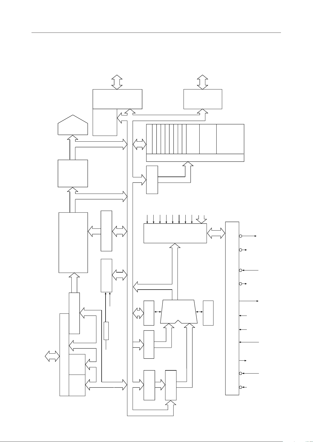
BLOCK DIAGRAM
(DATA
BUS
PORT)
(PORT 1)
PLA
INSTRUC-
TION
REGISTER
BUS
BUS LATCH
AND LOW
PC TEMP
REGISTER
8
BUFFER
MULTIPLEXER
REGISTER 0
REGISTER 1
REGISTER 2
RAM ADDRESS
REGISTER
TEST0
TEST1
INT
REGISTER 3
REGISTER 4
REGISTER 5
REGISTER 6
DECODER
FLAG0
FLAG1
TIMER FLAG
PORT1
BUS
REGISTER 7
8-LEVEL
STACK
CARRY
ACC
8
BUFFER
AND
LATCH
OPTIONAL
SECOND
REGISTER
BANK
ACC Bit TEST
DATA STORE
64¥8 bits MSM80C48RS
DATA MEMORY (RAM)
128¥8 bits MSM80C49RS
256¥8 bits MSM80C50RS
8
(PORT 2)
(ROM)
PROGRAM MEMORY
1K¥8bits MSM80C48RS
2K¥8bits MSM80C49RS
4K¥8bits MSM80C50RS
2 or 3
4
HIGHER PROGRAM
COUNTER (4)
8
PORT2 BUS BUFFER
PORT2
LATCH
(HIGH4)
44
PORT2 LATCH
(LOW4) AND
EXPANDER
PORT I/O
LOWER PROGRAM
COUNTER (8)
(8)
TIMER/EVENT
COUNTER (8)
TEST1
∏480
OSC FREQ
TEMP REG (8) FLAGS
ACCUMULATOR
(8)
CONDI-
TIONAL
BRANCH
LOGIC
(8)
UNIT
LOGIC
ARITHMETIC
ACCUMULATOR
LATCH (8)
ADJUST
DECIMAL
WRRDSSPSENALEXTAL2XTAL1EAPROGRESETINT
CONTROL AND TIMING
WRITE
STROBE
READ
STROBE
SINGLE
ENABLE
MEMORY
PROGRAM
ADDRESS LATCH,
XTAL
OSCILLATOR
CPU MEMORY
PROM/
STROBE
EXPANDER
INITIALIZE
INTERRUPT
STEP
CLOCK
DATA LATCH
STROBE CYCLE
SEPARATE
2/20
Page 3
¡ Semiconductor MSM80C48/49/50, MSM80C35/39/40
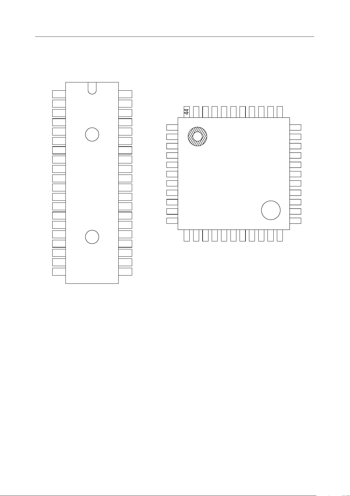
PIN CONFIGURATION (TOP VIEW)
T0
XTAL1
XTAL2
RESET
SS
INT
EA
RD
PSEN
WR
ALE
DB
DB
DB
DB
DB
DB
DB
DB
V
SS
1
2
3
4
5
6
7
8
9
10
11
12
0
13
1
14
2
15
3
16
4
17
5
18
6
19
7
20
40
39
38
37
36
35
34
33
32
31
30
29
28
27
26
25
24
23
22
21
V
CC
T1
P2
7
P2
6
P2
5
P2
4
P1
7
P1
6
P1
5
P1
4
P1
3
P1
2
P1
1
P1
0
V
DD
PROG
P2
3
P2
2
P2
1
P2
0
V
P1
P1
P1
P1
P1
P1
P1
P1
P2
DD
NC
35
21
NC
4
34
33
32
31
30
29
28
27
26
25
24
23
22
RESET
DB
3
DB
2
DB
1
DB
0
ALE
WR
PSEN
RD
EA
INT
SS
3P22P21P20
NC
44
PROG
P2
43
42
41
40
VSSDB7DB6DB5DB
39
38
37
36
1
2
0
3
1
4
2
5
3
6
4
7
5
8
9
6
10
7
11
4
12
13
14
15
16
17
18
19
20
NC
5P26P27
P2
T1
CC
T0
V
XTAL1
XTAL2
NC: No-connection pin
40-Pin Plastic DIP 44-Pin Plastic QFP
3/20
Page 4

¡ Semiconductor MSM80C48/49/50, MSM80C35/39/40
PIN DESCRIPTIONS
Symbol
-P1
P1
0
(PORT 1)
P20-P2
(PORT 2)
DB0-DB
(BUS)
T0
(Test 0)
T1
(Test 1)
Type Description
7
7
I/O
8-bit quasi-bidirectional portI/O
8-bit quasi-bidirectional port
The high-order four bits of external program memory addresses can be output
from P2.0-P2.3, to which the I/O expander MSM82C43RS may also be connected.
7
I/O
Bidirectional port
The low-order eight bits of external program memory address can be output
from this port, and the addressed instruction is fetched under the control of
PSEN signal. Also, the external data memory address is output, and data is
read and written synchronously using RD and WR signals.
The port can also serve as either a statically latched output port or a
non-latching input port.
I/O
The input can be tested with the conditional jump instructions JT0 and JNT0.
The execution of the ENT0 CLK instruction causes a clock output.
I
The input can be tested with the conditional jump instructions JT1 and JNT1.
The execution of a STRT CNT instruction causes an internal counter input.
INT
(Interrupt)
I
Interrupt input. If interrupt is enabled, INT input initiates an interrupt.
Interrupt is disabled after a reset.
Also testable with a JNI instruction. Can be used to terminate the power-down
mode. (Active "0" level)
RD
A signal to read data from external data memory. (Active "0" level)O
(Read)
WR
A signal to write data to external data memory. (Active "0" level)O
(Write)
ALE
O
Address &
Data Latch
Clock
PSEN Program
O
Store Enable
RESET RESET input initialize the processor. (Active "0" level)
I
This signal is generated in each cycle. It may be used as a clock output.
External data memory or external program memory is addressed upon the
falling edge. For the external ROM, this signal is used to latch the bus port data
upon the ALE signal rise-up after the execution of the OUTL BUS, A instruction.
A signal to fetch an instruction from external program memory
(Active "0" level)
Used to terminate the power-down mode.
SS
(Single Step)
I
A program is executed step by step. This pin can also be used to control
internal oscillation when the power-down mode is reset.
(Active "0" level)
EA
(External Access)
PROG
(Expander Strobe)
I
When held at high level, all instructions are fetched from external memory.
(Active "1" level)
This output strobes the MSM82C43RS I/O expander.O
4/20
Page 5

¡ Semiconductor MSM80C48/49/50, MSM80C35/39/40
PIN DESCRIPTIONS (Continued)
Symbol
XTAL1
(Crystal 1)
XTAL2
(Crystal 2)
V
CC
V
DD
V
SS
Type Description
One side of the internal crystal oscillator. An external clock can also be input.I
Other side of the internal crystal oscillator.O
Power supply pin—
—
Standby control input. Normally, "1" level. When set to "0" level, oscillation is
stopped and prosessor goes into standby mode.
GND—
Note: A minimum of two machine cycles are required in RESET pulse duration under the
specified power supply and stable oscillator frequency.
5/20
Page 6
¡ Semiconductor MSM80C48/49/50, MSM80C35/39/40
ABSOLUTE MAXIMUM RATINGS
Parameter Symbol
Supply Voltage V
Input Voltage V
Storage Temperature T
CC
I
STG
Condition Rating Unit
Ta=25°C –0.5 to 7 V
Ta=25°C –0.3 to V
— –65 to +150 °C
RECOMMENDED OPERATING CONDITIONS
Parameter Symbol
Supply Voltage V
Ambient Temperature T
CC
a
Fan Out N
* Minimum operating voltage is dependent on frequency.
Condition Range Unit
f
=DC to 11MHz* +2.5 to +6 V
OSC
— –40 to +85 °C
MOS load 10 —
TTL load 1 —
+0.5 V
CC
6/20
Page 7

¡ Semiconductor MSM80C48/49/50, MSM80C35/39/40
MSM80C48/49/50 guaranteed operating range
Ta=–40 to +85°C
(msec)
100
Guaranteed Operating Range
)
CY
10
Cycle Time (t
1
MSM80C40/80C50
MSM80C35/80C48/80C39/80C49
1.5MHz
6MHz
11MHz
Supply Voltage (VCC)
64532
(V)
7/20
Page 8

¡ Semiconductor MSM80C48/49/50, MSM80C35/39/40
ELECTRICAL CHARACTERISTICS
DC Characteristics
Parameter Symbol
"L" Input Voltage
"H" Input Voltage *1
"H" Input Voltage *2
"L" Output Voltage *3
"L" Output Voltage *4
"H" Output Voltage *3
"H" Output Voltage *4
"H" Output Voltage *3
"H" Output Voltage *4
Input Leakage Curent
Output Leakage Current *5
RESET Input current
SS Input current *6
P1, P2 input current
Power Down Mode
Standby Current
Power Supply Current
(Halt Mode)
Power Supply Current
=5 V±10%, Ta=–40 to +85°C)
(V
CC
Mea-
Condition Typ.Min. Max. Unit
V
IL
V
IH
V
IH
V
OL
V
OL
V
OH
V
OH
V
OH
V
OH
I
IL
I
OL
I
R
— –0.5 —
—
—
0.4 V
0.7 V
CC
CC
0.13 V
CC
—VCCV
—VCCV
IOL=2 mA — — 0.45 V
IOL=1.6 mA — — 0.45 V 1
IOH=–400 mA
IOH=–50 mA
IOH=–20 mA
IOH=–10 mA
VSS £ VIN £ V
VSS £ VO £ V
VIN=0.7 V
=0.13 V
V
IN
CC
CC
CC
CC
0.75 V
0.75 V
0.93 V
0.93 V
—— V
CC
—— V
CC
—— V
CC
—— V
CC
——±5mA2
——±5mA3
–20 –50 –80 mA
–3 –8 –15 mA
suring
Circuit
V
2
Pull-up (VIN=VIL) 205080mA
I
SS
Pull-down (V
VIN=V
, I
I
P1
P2
V
IN=VIL
At hardware power down
I
CCS
Ta=25°C, VCC=2.0 V
At HLTS execution
Ta=25°C, VCC=2.0 V
=4 V, f=1 MHz — — 0.5
V
CC
=4 V, f=6 MHz — — 1.0
V
CC
=4 V, f=11 MHz — — 2.0
V
CC
=5 V, f=1 MHz — — 1.0
V
CC
I
CC
I
CC
VCC=5 V, f=6 MHz — — 2.0 mA
=5 V, f=11 MHz — — 3.0
V
CC
=6 V, f=1 MHz — — 1.5
V
CC
=6 V, f=6 MHz — — 3.0 4
V
CC
=6 V, f=11 MHz — — 5.0
V
CC
=4 V, f=1 MHz — — 1.5
V
CC
=4 V, f=6 MHz — — 5.0
V
CC
=4 V, f=11 MHz — — 10
V
CC
=5 V, f=1 MHz — — 2.5
V
CC
VCC=5 V, f=6 MHz — — 7.5 mA
=5 V, f=11 MHz — — 15
V
CC
=6 V, f=1 MHz — — 5.0
V
CC
=6 V, f=6 MHz — — 10
V
CC
=6 V, f=11 MHz — — 20
V
CC
) –6 –15 –25 mA
IN=VIH
IH
–300 –600 –900 mA
–10 –40 –80 mA
*7
——10
*7
——10
2
mA
8/20
Page 9

¡ Semiconductor MSM80C48/49/50, MSM80C35/39/40
*1 This does not apply to RESET, XTAL1, XTAL2, VDD, and EA.
*2 RESET, XTAL1, XTAL2, VDD, and EA.
*3 BUS, RD, WR, PSEN, ALE, PROG
*4 Other outputs
*5 High-impedance state
*6 This operates as a pull-down resistor when the oscillation is stopped in the HLTS or V
DD
power-down mode and as a pull-up resistor in other states.
*7 This does not contain flow out current from I/O ports and signal pins.
9/20
Page 10

¡ Semiconductor MSM80C48/49/50, MSM80C35/39/40
AC Characteristics
(VCC=2.5V to 6V (*1), Ta=–40 to +85°C)
V
Parameter Symbol
ALE Pulse Width
Address Setup Time (up to ALE)
Address Hold Time (from ALE)
Bus Port Latch Data Setup Time (up to ALE Rising Edge)
Bus Port Latch Data Hold Time (from ALE Rising Edge)
Control Pulse Width (RD, WR)
Control Pulse Width (PSEN)
Data Setup Time (before WR)
Data Hold after Time (after WR)
Data Hold Time (after RD, PSEN)
RD to Data-in
PSEN to Data-in
Address Setup to WR
Address Setup to Data-in
Address Setup to Instruction
Address Float to RD, WR
Address Float to PSEN
Control Pulse Setup Time from ALE (PSEN)
Control Pulse Setup Time from ALE (RD, WR)
Control Pulse up to ALE (RD, WR, PROG)
Control Pulse up to ALE (PSEN)
Port Control Setup Time (up to PROG Falling Edge)
Port Control Hold Time (from PROG Falling Edge)
PROG to Input Data Valid
Input Data Hold Time
Output Data Setup Time
Output Data Hold Time
PROG Pulse Width
Port 2 I/O Setup Time
Port 2 I/O Hold Time
Port Output Data (from ALE)
T0 Cycle
Instruction Execution Time
t
LL
t
AL
t
LA
t
BL
t
LB
t
CC1
t
CC2
t
DW
t
WD
t
DR
t
RD1
t
RD2
t
AW
t
AD1
t
AD2
t
AFC1
t
AFC2
t
LAFC2
t
LAFC1
t
CA1
t
CA2
t
CP
t
PC
t
PR
t
PF
t
DP
t
PD
t
PP
t
PL
t
LP
t
PV
t
OPRR
t
CY
=5 V±10%
CC
11 MHz Clock
Min. Max. Min. Max.
150 — 3.5t–170 — ns
70 — 2t–110 — ns
50 — t–40 — ns
110 — 2.5t –115 — ns
90 — 1.5 t–45 — ns
480 — 7t–155 — ns
350 — 6t–200 — ns
390 — 6t–155 — ns
40 — 2t–140 — ns
0 110 0 1.5t–30 ns
— 350 — 5t–265 ns
— 190 — 5t–265 ns
300 — 6t–245 — ns
— 730 — 12t–360 ns
— 460 — 8t–265 ns
140 — 2t–40 — ns
10 — 10 — ns
60 — t–30 — ns
200 — 3t–75 — ns
50 — 1.5t–85 — ns
320 — 4.5t–90 — ns
50 — 2t–130 — ns
100 — 4t–260 — ns
— 650 — 9t–170 ns
0 140 0 1.5t ns
250 — 6t–290 — ns
40 — 3t–230 — ns
700 — 10t–210 — ns
160 — 4.5–250 — ns
15 — 1.5t–120 — ns
— 510 — 4t+145 ns
270 — 3t — ns
1.36 — 15t — ms
Variable clock
0 to 11 MHz
Unit
Note : Control output : CL=80pF
Bus output : CL=150pF [for 20 pF (tAL, t
AFC1
, t
AFC2
*1 Minimum operating voltage is dependent on frequency.
)]
10/20
Page 11

¡ Semiconductor MSM80C48/49/50, MSM80C35/39/40
Measuring circuits
1
V
CC
V
IH
(*3)
V
IL
INPUTS
GND
(*2)
OUTPUT
V A
(*1)
I
O
A
3
2
V
CC
INPUTS
GND
4
OUTPUT
A
V
CC
V
IH
(*3)
V
IL
INPUTS
GND
OUTPUT
A
V
IH
(*3)
V
IL
V
CC
INPUTS
GND
OUTPUT
5
V
CC
V
IH
(*3)
V
IL
INPUTS
GND
(*2)
CL
OUTPUT
*1 This is repeated for each specified input pin.
*2 This is repeated for each specified output pin.
*3 Input logic for setting the specified state
V
IH
I
V
OH
O
V
IL
V
OL
O
V
t
XXX
V
OL
t
OH
XXX
11/20
Page 12

¡ Semiconductor MSM80C48/49/50, MSM80C35/39/40
Timing Diagram
Instruction fetch (from external program memory)
t
CY
t
LL
ALE
t
AFC
t
CC
PSEN
tALt
t
LA
RD
t
DRtBLtLB
BUS
LATCH DATA FLOATING INSTRUCTION LATCH DATA
Read (from external data memory)
ALE
RD
BUS
ADDRESS
ADDRESS
t
t
AD
AD
t
AFC
FLOAT-
ING
ADDRESS
t
CC
t
RD
DATA
t
DR
FLOAT-
ADDRESS
ING
12/20
Page 13

¡ Semiconductor MSM80C48/49/50, MSM80C35/39/40
Write (to external memory)
ALE
t
CC
WR
t
AW
t
DW
t
WD
BUS
ADDRESS
FLOAT-
ING
DATA ADDRESS
Low-order 4 bits input/output of port 2 when expanded I/O port is used
(in external program memory access mode)
ALE
t
LP
P2
0-3
(Output mode)
PCH
t
PL
PORT DATA PORT CONTROL OUTPUT DATA
t
DP
t
PD
P2
0-3
(Input mode)
PROG
PCH PORT DATA PORT CONTROL
t
t
CP
PC
t
PR
t
PF
INPUT
DATA
t
PP
13/20
Page 14

¡ Semiconductor MSM80C48/49/50, MSM80C35/39/40
FUNCTIONAL DESCRIPTION
Added Functions of MSM80C48, MSM80C49 and MSM80C50
The MSM80C48, MSM80C49 and MSM80C50 are basically incorporated with the capabilities of
Intel's 8048, 8049, and 8050 plus the following new functions:
1. Power-Down Mode Enhancements
1.1 Power-down by software
(1) Clock (See item 4, "Power-down mode", for details.)
a. Crystal oscillator halt (HLTS instruction)
Power requirements can be minimized.
b. Clock supply halt (HALT instruction)
Restart is accomplished without oscillator wait.
(2) I/O ports
I/O port floating instructions
Power consumption resulting from inputs/outputs can be minimized with FLT and FLTT
instructions.
Port floating is cancelled by executing FRES instruction, "0" level at INT pin or "0" level at
RESET pin.
(3) Six types of power-down can be done by a combination of HLTS/HALT and FLT/FLTT
instructions.
1.2 Power-down by hardware (See 4.3, Power-down mode by VDD pin utilization for
details.)
Crystal oscillators can be halted by controlling the V
pin, thereby floating all I/O ports
DD
for minimum power consumption.
2. Additional Instructions (11)
HLTS MOV A, P2
HALT MOVP1, @ R3
FLT MOVP1 P, @R3
FLTT DEC @Rr
FRES DJNZ @ Rr, addr
MOV A, P1
3. Improved Uses of BUS P0-7, P10-7, P20-7, and SS pins
3.1 BUS P0-
7
The MSM80C48, MSM80C49, and MSM80C50 remove the limitation on the use of OUTL
BUS, A instructions during the external ROM access mode by having an independent data
latch and external ROM mode address latch in BUS P0-7.
Consequently, there is no need to relocate bus port instructions when in the external ROM
access mode.
3.2 P10-7 and P20-
7
The MSM80C48, MSM80C49 and MSM 80C50 are designed to minimize power consumption
when P10-7 and P20-7 are used as input/output ports, to maximize the performance of
CMOS.
When these ports are used as output ports, the acceleration circuit is actuated only when
14/20
Page 15

¡ Semiconductor MSM80C48/49/50, MSM80C35/39/40
output data changes from "0" to "1", thus speeding up the rise time of the output signals.
When these ports are used as input ports, the internal pull-up resistor becomes approximately
9 kW when input data is "1".
The internal pull-up resistor rises to approximately 100 kW when input data is "0".
Thus, a high noise margin can be obtained by selecting the impedance and thus the outflow
of current is minimized whenever these ports are used as output or input ports.
3.3 Clock generation control via the SS pin
When the crystal oscillator is halted in the HLTS or hardware power-down mode, the SS
pin is pulled down by a resistor of 20 to 50 kW, while its internal pull-up resistor of 200 to
500kW is isolated from VCC. When the power-down mode is cancelled, the internal resistor
of the SS pin is changed from pull-down to pull-up. Consequently, the CPU can be halted
for any period of time until the crystal oscillator resumes normal oscillation when a
capacitor is connected to the SS pin.
4. Power-Down Mode
The MSM80C48, MSM80C49, and MSM80C50 power-down mode can be enabled in two
different ways through software by a combination of clock control and port floating
instructions, and through hardware by control of the VDD pin.
4.1 Software power-down mode
Power-down mode can be done by a combination of the following instructions.
(1) HALT (clock supply halt to control circuit)
Instruction code :
00000001
Description : Although crystal oscillator operation is continued, the clock supply to
the CPU control circuit is halted and CPU operations are suspended.
When cancelling this software mode, restart is accomplished without
oscillator wait.
(2) HLTS (oscillation stop)
Instruction code :
10000010
Description : The oscillator operation is halted and CPU operations are suspended. In
cancelling this power down mode, connecting a capacitor to the SS pin
enables a reasonable wait period to be accomplished before normal
operation is resumed. [Except in the case of using the RESET pin]
(3) FLT (floating P10-7, P20-7, and BP0-7)
Instruction code :
10100010
Description :
P1
P2
BP
Internal ROM mode
Floating
Floating
Floating
External ROM mode
Floating
operation
P2
0-3
Operation
15/20
Page 16

¡ Semiconductor MSM80C48/49/50, MSM80C35/39/40
Details of IC pin status as a result of executing the FLT instruction are shown in the above table.
(4) FLTT (floating of all output pins)
Instruction code :
Description :
11000010
Internal ROM mode
ALE
PSEN
PROG
WR
PD
T0 OUT
P1
P2
BP
XTAL
Floating
Floating Operation
Floating Floating
Floating Floating
Floating Floating
Floating Floating
Floating Floating
Floating
Floating Operation
Operation
External ROM mode
Operation
operation
P2
0-3
Operation
Details of IC pin status as a result of executing the FLTT instruction are shown in above
Table.
Example 1 : Power-down mode accomplished by stopping oscillation.
m Can be set by execution of HLTS [82H] instruction.
Example 2 : Power-down mode accomplished by stopping the clock supply to the CPU
control circuit.
m Can be set by execution of HALT [01H] instruction.
Example 3 : Power-down mode by floating of P10-7, P20-7 and BP0-7, and subsequent
stopping of CPU oscillation.
m Can be set by first executing the FLT [A2H] instruction, followed by the
HLTS [82H] instruction.
Example 4 : Power-down mode by floating P10-7, P20-7 and BP0-7, and then stopping the
clock supply to the CPU control circuit.
m Can be set by first executing the FLT [A2H] instruction, and then the HALT
[01H] instruction.
Example 5 : Power-down mode by floating all output pins, followed by stopping oscillation.
m Can be set by first executing the FLTT [C2H] instruction followed by
execution of the HLTS [82H] instruction.
Example 6 : Power-down mode by floating all output pins, followed by stopping of the
clock supply to the CPU control circuit.
m Can be set by first executing the FLTT [C2H] instruction, followed by
execution of the HALT [01H] instruction. Connect the pull-up resistor or
pull-down resistor to port pin and fix the output port pin level to either 1or
0 when output port is set to floating.
16/20
Page 17

¡ Semiconductor MSM80C48/49/50, MSM80C35/39/40
4.2 Cancellation of software power-down mode
The power-down mode status outlined above in examples 1 to 6 can be cancelled by using
either the interrupt pin or the RESET pin.
(1) Use of the INT pin during external interrupt enable mode (i.e. following execution of
EN I instruction).
m The clock generator is activated and the CPU is started up when a "0" level is
applied to the INT pin. If this "0" level is maintained until the occurrence of at least
2 ALE output signals, an external interrupt is generated, and execution proceeds
from address 3. If, however, the power-down is entered during the interrupt
processing routine, execution resumes just after the power-down instruction.
(2) Use of the INT pin during external interrupt disable mode (i.e. following execution of
DIS I instruction or hardware reset)
m The clock generator is activated and the CPU is started up when a "0" level is
applied to the INT pin. When "0" level is maintained until the occurrence of at least
2 ALE output signals, execution is resumed just after the power-down instruction.
(3) Use of the RESET pin
m The clock generator is activated and the CPU started up when a "0" level is applied
to the RESET pin. If this "0" level is maintained until the occurrence of at least 2 ALE
output signals, the CPU is reset and execution proceeds from address 0. In case
cancellation is done in oscillation stop mode, the "0" level must be input to the
RESET pin until oscillation is stabilized.
17/20
Page 18

¡ Semiconductor MSM80C48/49/50, MSM80C35/39/40
4.3 Hardware power-down mode
In the MSM80C48, MSM80C49 and MSM80C50, forcing the level at the VDD pin to a "0"
during either external ROM or internal ROM mode results in suspension of the oscillator
function and subsequent floating (high impedance) of all the I/O pins except the RESET,
SS and XTAL 1/2 pins. The CPU is thereby stopped while maintaining internal status.
4.4 Cancellation of hardware power-down mode
(1) Use of RESET pin
m The clock generator is activated and the CPU started up when a "1" level is applied to
the VDD pin while a "0" level is input to the RESET pin. If this "0" level is kept applied
to the RESET pin until oscillation become stable, the CPU will be reset and will start
executing from address 0.
(2) Use of the INT pin during external interrupt enable status (i.e. following execution of EN
I instruction)
m The clock generator is activated and the CPU started up when a "1" level is applied to
the VDD pin while a "0" level is applied to the INT pin. If this "0" level is maintained
until the occurrence of at least 2 ALE output signals, an external interrupt is generated,
and execution starts from address 3.
However, if the power-down mode is started during an interrupt processing routine,
execution will be continued on the next instruction after the present instruction.
(3) Use of the INT pin during external interrupt disable mode (i.e. following excution of DIS
I instruction or hardware reset)
m The clock generator is activated and the CPU started up when a "1" level is applied to
the VDD pin while a "0" level is applied to the INT pin. If this "0" level is maintained
until the occurrence of at least 2 ALE output signals, execution is continued on the next
instruction after the present instruction.
(4) Use of VDD pin only
m The clock generator is activated and the CPU started up when a "1" level is applied to
the VDD pin while a "1" level is also applied to both the RESET and INT pins. In this
case, execution is resumed from the stopped position.
18/20
Page 19

¡ Semiconductor MSM80C48/49/50, MSM80C35/39/40
PACKAGE DIMENSIONS
(Unit : mm)
DIP40-P-600-2.54
Package material
Lead frame material
Pin treatment
Solder plate thickness
Package weight (g)
Epoxy resin
42 alloy
Solder plating
5 mm or more
6.10 TYP.
Notes for Mounting the Surface Mount Type Package
The SOP, QFP, TSOP, SOJ, QFJ (PLCC), SHP and BGA are surface mount type packages, which
are very susceptible to heat in reflow mounting and humidity absorbed in storage.
Therefore, before you perform reflow mounting, contact Oki’s responsible sales person for the
product name, package name, pin number, package code and desired mounting conditions
(reflow method, temperature and times).
19/20
Page 20

¡ Semiconductor MSM80C48/49/50, MSM80C35/39/40
(Unit : mm)
QFP44-P-910-0.80-2K
Mirror finish
Package material
Lead frame material
Pin treatment
Solder plate thickness
Package weight (g)
Epoxy resin
42 alloy
Solder plating
5 mm or more
0.41 TYP.
Notes for Mounting the Surface Mount Type Package
The SOP, QFP, TSOP, SOJ, QFJ (PLCC), SHP and BGA are surface mount type packages, which
are very susceptible to heat in reflow mounting and humidity absorbed in storage.
Therefore, before you perform reflow mounting, contact Oki’s responsible sales person for the
product name, package name, pin number, package code and desired mounting conditions
(reflow method, temperature and times).
20/20
 Loading...