

Page 1

FEDL7731-02-04
1
Semiconductor
This version: Jan. 2000
Previous version: Jan. 2000
MSM7731-02
Dual Echo Canceler & Noise Canceler with Dual Codec for Hands-Free
1/53
GENERAL DESCRIPTION
The MSM7731 is an IC device developed for portable, handsfree communication with built-in line echo canceler,
acoustic echo canceler, and transmission signal noise canceler. Built-in to the voice signal interface is a linear
CODEC for the analog interface on the acoustic-side, and a linear CODEC for the analog interface on the line-side.
On the line-side, in addition to the analog interface, there is also a µ-law PCM/16-bit linear digital interface.
Equipped with gain and mute controls for data transmission and reception, a µ-law PCM/16-bit linear digital
interface for memo recording and message output, and transfer clock and sync clock generators for digital
communication, this device is ideally suited for a handsfree system.
FEATURES
• Single 3 V Power Supply Operation (2.7 to 3.6 V)
• Built-in 2-channel (line and acoustic) echo canceler
Echo attenuation : 35 dB (typ.) for white noise
Cancelable echo delay time :
Line echo canceler + acoustic echo canceler : Tlined = 27 ms (max.)
Tacoud = 59 ms – Tlined (max.)
Acoustic echo canceler only : Tacoud = 59 ms (max.)
• Built-in transmission signal noise c anceler
Noise attenuation : 17 dB (typ.) for white noise
40 dB (typ.) for single tone
• Built-in 2-channel CODEC
Synchronous transmission and reception enables full duplex operation
• Built-in analog input gain amp stage (max. gain = 30 dB)
• Analog output configuration : Push-pull drive (can drive a 1.2 k
Ω
load
)
• Built-in transmit slope filter
• Digital interface coding formats : µ-law PCM, 16-bit linear (2's complement)
• Digital interface sync formats : Normal-sync, short-frame-sync
• Built-in digital transmission clock generators
Sync clock (S YNC) : 8 kHz output
Transmission clock (BCLK) : 64 kHz output (µ-law PCM)/128 kHz output (16-bit linear)
• Digital transmission rate
External input : 64 to 2048 kbps
Internal generation : 64 kbps (µ-law PCM)/128 kbps (16-bit linear)
• Fixed digital interface sync clock (SYNC) enables automatic power-down
• Master clock frequency : 19.2 MHz
Compatible with crystal oscillator and crystal
• Low power consumption
Operating mode : typ. 35 mA (when V
DD
= 3.0 V in a silent mode)
Power down operation : typ. 0.02 mA (when V
DD
= 3.0 V in a silent mode)
• Control by both the serial microcomputer interface and parallel port is possible
• Transmit/receive mute function, transmit/receive programmable gain setting
• Package : 64-pin plastic QFP (QFP64-P-1414-0.80-BK)(Product name: MSM7731-02GA)
Page 2
FEDL7731-02-04
1
Semiconductor
MSM7731-02
2/53
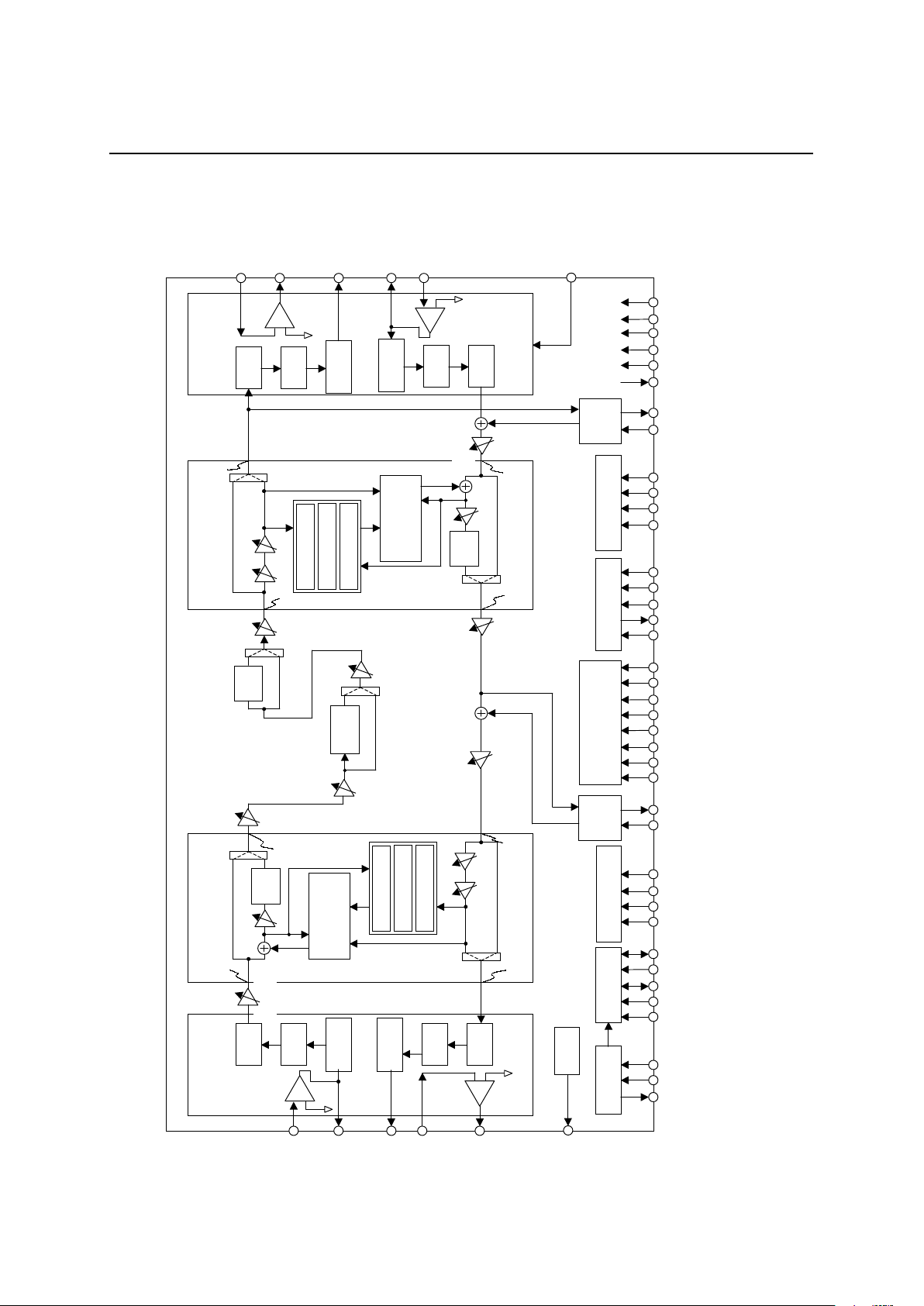
BLOCK DIAGRAM
AIN
AGSX
AVFRO
APWI
AOUT
SG
Linear Codec
(Acoustic side)
BPF
ADC
RC LPF
RC LPF
DAC
LPF
VREF
Clock Gen Timing Gen AEC Controller
P/S
&S/P
EC/NC/SF/PAD
Controller
MCU Interface LEC Controller
P/S
&S/P
–
+
–
+
1.2 k
Ω
LPADA
GPADA
GPADNC
RPAD GPADL
LPADNC
TPAD
ATTsA
Center
Chip
Power
Calc
.
Howling Detector
Double Talk Det
Acoustic
Adaptive
FIR
Filter
(
AAFF
)
RoutA
RinA
GainA ATTrA
SinA
SoutA
Slope
Filter
Noise
Canleler
ATTrL GainL
Power
Calc
.
Howling Detector
Double Talk Det
Line
Adaptive
FIR
Filter
(
LAFF
)
Center
Chip
RinL
RoutL
SinLSoutL
ATTsL
–
+
–
+
–
+
LPADL
LPWI
DAC
RC LPF
RC LPF
ADC
BPF
1.2 k
Ω
Acoustic Echo
Canceler
Line Echo
Canceler
Linear Codec
(Line side)
LOUT
LVFRO
LGSX
LIN
LINEEN
AGND
AVDD
DGND1,2
DVDD1,2
TEST1-4
TEST9
PCMO
PCMI
LTHR
LGC
LATT
LHD
D
EN
EXCK
DIN
DOUT
MCUSEL
NCPAD1,2
NCSEL1,2
RPAD1-4
TPAD1-4
ECSEL
GLPADTHR
SLPTHR
RST
PCMEO
PCMEI
ATHR
AGC
AATT
AHD
SYNC
SYNCSEL
BCLK
CLKSEL
PCMSEL
P
DN/RST
MCK/X1
X2
LPF
+
-
Page 3
FEDL7731-02-04
1
Semiconductor
MSM7731-02
3/53
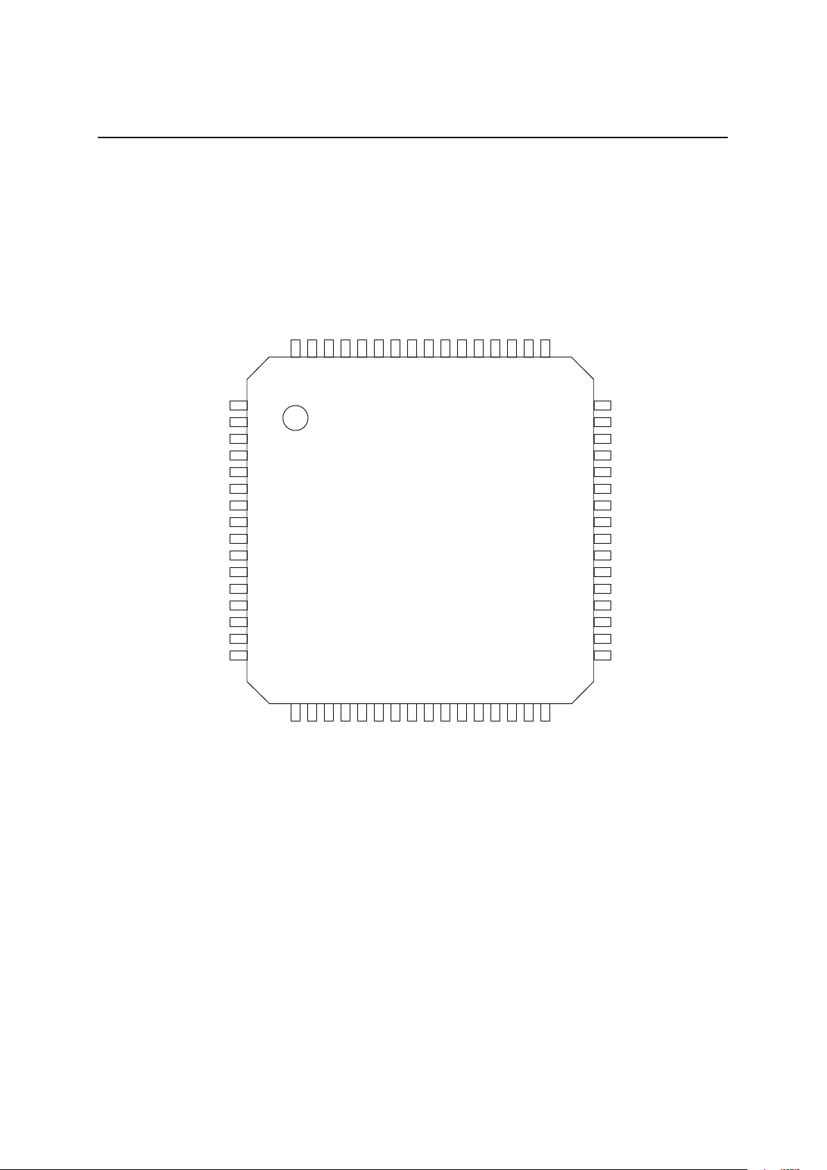
PIN CONFIGURATION (TOP VIEW)
64-Pin Plastic QFP
EXCK
DIN
NCSEL1
SLPTHR
TEST1
TEST2
TEST3
TEST4
NCSEL2
PDN/RST
RST
SYNC
BCLK
CLKSEL
PCMI
PCMEI
PCMEO
PCMO
PCMSEL
SYNCSEL
DOUT
DEN
DVDD2
GLPADTHR
TEST9
LINEEN
AGND
LOUT
LPWI
LVFRO
LGSX
LIN
48
47
46
45
44
43
42
41
40
39
38
37
36
35
34
33
646362616059585756555453525150
49
171819202122232425262728293031
32
1
2
3
4
5
6
7
8
9
10
11
12
13
14
15
16
RPAD2
RPAD1
DGND2
TPAD4
TPAD3
TPAD2
TPAD1
MCK/X1
X2
AVDD
AGS
X
AIN
AVFRO
APWI
AOU
T
SG
ECSEL
MCUSEL
AHD
NCPAD2
AATT
AGC
DGND1
ATHR
LHD
NCPAD1
LATT
LGC
LTHR
RPAD4
DVDD1
RPAD3
Page 4
FEDL7731-02-04
1
Semiconductor
MSM7731-02
4/53
PIN FUNCTIONAL DESCRIPTION
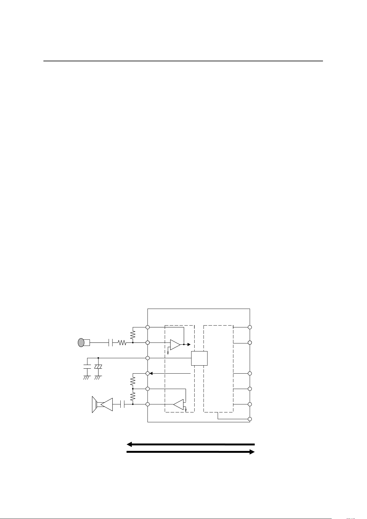
AIN, AGSX
These are the acoustic analog input and level adjusting pins. The A IN pin is conn ected to the inverting input of the
internal amp and the AGSX pin is connected to the amp output. For level adjustment, refer to the diagram below
(Figure 1). At power-down reset, the AGSX pin goes to a high impedance state.
AVFRO, AOUT, APWI
These are acoustic analog output and level adjusting pins. The AVFRO pin is an audio output and can directly
drive 20 kΩ. The AOUT pin is an analog output and can directly drive a load of 1.2 kΩ. For level adjustment, refer
to the diagram below (Figure 1). At power-down reset, these output pins go to a high impedance state.
LIN, LGSX
These are the line analog input and level adjusting pins. The LIN pin is connected to the inverting input of the
internal amp and the LGSX pin is connected to the amp output. For level adjustment, refer to the diagram below
(Figure 1). At power-down reset, the LGSX pin goes to a high impedance state. If LIN is not used, short the LIN
and LGSX together.
LVFRO, LOUT, LPWI
These are acoustic analog output and level adjusting pins. The LV FRO pin is an audio output and can directly drive
20 kΩ. The LOUT pin is an analog output and can directly driv e a load of 1.2 kΩ. For level adjustment, refer to the
diagram below (Figure 1). At power-down reset, these output pins go to a high impedance state. If LOUT is not
used, short the LPWI and LOUT pins together.
LINEEN
LINEENLINEEN
LINEEN
This is the power-down control pin for the line CODEC. A logic “0” continues normal operation and a logic “1”
power down only the line C ODEC. If the line CODEC is not used, pow er down the line CODEC and s hort th e LIN
pin to the LGSX pin and the LPWI pin to the LOUT pin. This procedure results in the low consumption of
electrical power. At power-down, the output pins go to a high impedance state. If the pin setting is changed, reset
must be activated by either the
PDN/RST
pin or the PDN/RS T bit (CR0-B7). This pin is ORed w ith CR0-B5 of th e
control register. Refer to the section “RELATIONSHIP BETWEEN PINS AND CONTROL REGISTERS”.
Figure 1 Analog Interface
Acoustic CODEC
C1
+
R1
MIC
0.1 µF
10 µF
–
R2
R3
R4
Line CODEC
V
AGSX
/Vi = R2/R1 ≤ 30
V
AGSX
= 1.3 V
PP
R2 ≥ 20 k
Ω
V
O/VAVFRO
= R4/R3 ≤ 2
V
O
= 2.6 VPP,
V
AVFRO
= 1.3 V
PP
R3, R4 ≥ 20 k
Ω
C2
SP
SPamp
Vo
Vi
AGSX
AIN
SG
AVFRO
APWI
AOUT
to ENCODER
LGSX
LIN
LVFRO
LPWI
LOUT
VREF
LINEEN
Receive Signal
Transmit Signal
Line Side (Hand Set)
Acoustic Side (Mic, Speaker)
Same as acoustic
analog interface
–
–
+
+
Page 5
FEDL7731-02-04
1
Semiconductor
MSM7731-02
5/53
AGND
This is analog ground pin.
DGND1, DGND2
These are the digital ground pins.
AV
DD
This is the analog +3 V power supply pin.
DV
DD1
, DV
DD2
These are the digital +3 V power supply pins.
SG
This is the output pin for the analog signal ground potential. The output voltage is approximately 1.4 V.
Insert 10 µF and 0.1 µF ceramic bypass capacitors between the AGND and SG p in. At power-down rest, this
output becomes 0 V.
PDN
PDNPDN
PDN/RST
RSTRST
RST
This is the power-down reset control input pin. If a logic “0” is input to this pin, the device enters the power-down
state. At this time, all control register bits, internal variables, and coefficients of echo cancelers and noise cancelers
will be reset. After the power-down reset state is released, the device enters the initial mode (refer to the CR0
control register description). During normal operation, set this pi n to a logic “1”. The
PDN/RST
pin is ORed
(negative logic) with CR0-B7 of the control register. Refer to the section “RELATIONSHIP BETWEEN PINS
AND CONTROL REGISTERS”.
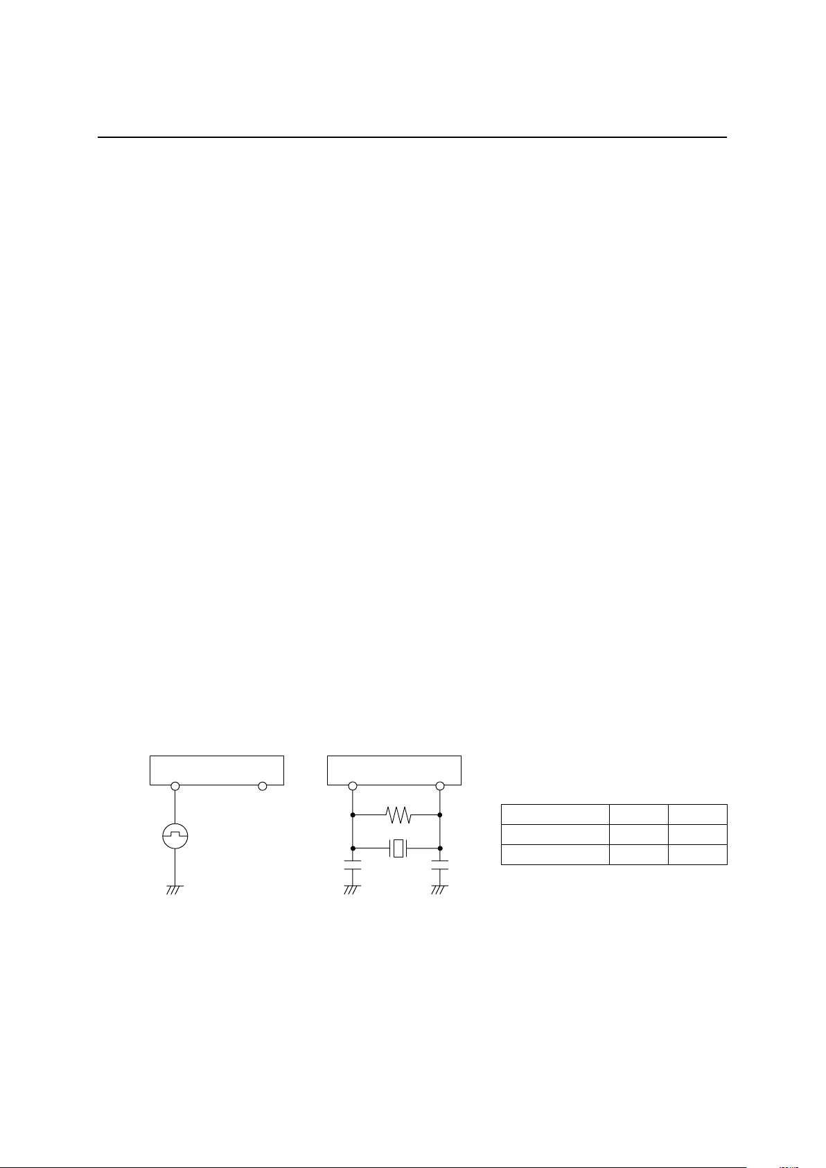
MCK/X1
This is the master clock input pin. The clock frequency is 19.2 MHz. The input clock may be asynchronous with
respect to the SYNC signal or the BCLK signal. Refer to Figure 2 (a) for an example application of an external
clock and Figure 2 (b) for an example oscillator circuit.
X2
This is the crystal oscillator output pin. If an existing external clock is to be used, leave this pin open and input the
clock to the MCK pin. Refer to Figure 2 (b) for an example oscillator circuit.
X’tal (19.2 MHz) C R
HC-49/U 10 pF 1 M
Ω
CX-91F T.B.D T.B.D
Figure 2 (a) External Clock Figure2 (b) Oscillator Circuit
Application Example Example
MCK/X1 X2
C
MCK/X1
X2
C
X’tal
R
Page 6

FEDL7731-02-04
1
Semiconductor
MSM7731-02
6/53
SYNC
This is the 8 kHz sync signal I/O pin for digital data communication. This pin is switched to unction as an input or
output by the CLKSEL pin. If the internal clock mode is selected by the CLKSEL pin, an 8 kHz clock
synchronized to be BCLK signal is output and digital data communication is performed. If the external clock mode
is selected by the CLKSEL pin, this pin becomes an input that requires an 8 kHz clock input synchronized to be
BCLK pin, and digital data communication is performed based on this input clock. This pin enables automatic
power-down control. Fixing this pin to a logic “1” or logic “0” causes this device to enter the power-down state.
Two kinds of power-down modes can be selected by the SYPDN (CR11-B0) bit of the control register. For the
power-down mode, refer to the description of control register CR11.
BCLK
This is the shift clock I/O pin for digital data communication. This pin is switched to function as an input or output
by the CLKSEL pin. If the internal clock mode is selected by the CLKSEL pin, a 64 kHz or 128 kHz clock
synchronized to the SYNC signal is outp ut and digital data communication is p erformed. Switc hing between 6 4
kHz and 128 kHz is performed by the PCMSEL pin or PCMSEL (CR11-B1) bit. If µ-law PCM is selected by the
PCMSEL pin or PCMSEL bit, a 64 kHz clock is output. Or, if 16-bit linear mode is selected, a 128 kHz clock is
output. If the external clock mode is selected by the CLKSEL pin, this pin becomes an input that requires a clock
input synchronized to the SYNC. In this case, the clock frequency range is from 64 kHz to 2048 kHz.
CLKSEL
This pin selects internal or external clock modes for the SYNC and BCLK signals. A logi c “ 0” selects the intern al
clock mode. At this time, SYNC and BCLK pins are con figured as ou tput pins and each intern ally generated clock
is output to perform digital data communication. A logic “1” selects the external clock mode and configures the
SYNC and BCLK pins as input pins. At this time, digital data communication is performed with the externally
input SYNC and BCLK clocks. If digital data communication is not used, set this pin to a logic “0” to select
internal clocks. If the pin setting is changed, reset must be activated by either the
PDN/RST
pin or the PDN/RST
bit (CR0-B7).
PCMI
This is the digital receive signal input pin on the line-side. This input signal is shifted at the rising edge of the
BCLK signal and input. The beginning of digital data is identified on the rising edge of the SYNC signal. The
coding format can be selected as µ-law PCM or 16-bit linear (2’s complement) by the PCMSEL pin or PCMSEL
(CR11-B1) bit. If the PCMI pin is not used, set it to a logic “1” if µ-law PCM has been selected, or a logic “0” if
16-bit linear mode has been selected. The sync format can be selected as normal-sync or short-frame-sync by the
SYNCSEL pin. Refer to Figure 3 for the timing. This digital input signal is added internally to the CODEC digital
output signal. Be careful of overflow when using the CODEC.
PCMO
This is the digital transmit signal output pin on the line-side. This output signal is synchronized to the rising edge
of the BCLK and SYNC signals and then output. Wh en not used f or output , this pin is in the h igh impedance state.
It is at high impedance during the power-down reset and the initial modes. The coding format can be selected as
µ
-law PCM or 16-bit linear (2’s complement) by the PCMSEL pin or PCMSEL (CR11-B1) bit. The sync format
can be selected as normal-sync or short-frame-sync by the SYNCSEL pin. Refer to Figure 3 for the timing.
Page 7

FEDL7731-02-04
1
Semiconductor
MSM7731-02
7/53
PCMEI
This is the massage signal input pin. Use this pin when a massage is output to the speaker on the acoustic-side. This
input signal is shifted at the rising edge of the BCLK signal and then input. The beginning of digital data is
identified on the rising edge of the SYNC sign al. The coding format can be selected as µ-law PCM or 16-bit linear
(2’s complement) by the PCMSEL pin or PCMSEL (CR11-B1) bit. If the PCMEI pin is not used, set it to a logic
“1” if µ-law PCM has been selected, or a logic “0” if 16-bit linear m ode has been se lected. The sync format can be
selected as normal-sync or short-frame sync by the SYNCSEL pin. Timing is the same as for the PCMI pin (refer
to Figure 3). This dig i tal inpu t sign al is added internally to the echo can celer ou t put s ig n al. Be careful of overflow
during telephone conversations.
PCMEO
This output pin is for memo recording. Use it with the memo function. This output signal is synchron ized to the
rising edge of t he BCLK an SYNC signals a nd then output. When not used for output, this pin is in the high
impedance state. It is also at high impedance during the power-down reset and the initial modes. The coding format
can be selected as µ-law PCM or 16-bi t l inear (2’s complement) by the PCMSEL pin or PCMSEL (CR 11-B1) bit.
The sync format can be selected as normal-sync or short-frame-sync by the SYNCSEL pin. Timing is the same as
for the PCMO pin (refer to Figure 3).
SYNCSEL
This is the sync timing selection pin for digital data communication. A logic “0” selects normal-sync timing and a
logic “1” selects short-frame-sync timing. Refer Figure 3 for the timing. If the pin setting is changed, reset must be
activated by either the
PDN/RST
pin or the PDN/RST bit (CR0-B7)
PCMSEL
This is the coding format selection pin for digital data communication. A logic “1” selects µ-law PCM and a logic
“0” selects 16-bit linear (2’s complement) coding format. When an internal clock is selected, the BCLK signal
determines the output clock frequency. If the digital interface is not used, set this pin to logic “0” to select 16-bit
linear coding format.
If the pin setting is changed, reset must be performed by either the
PDN/RST
pin or the PDN/RST bit (CR0-B7).
This pin is logically ORed with the PCMSEL bit (CR11-B1). Refer to the section “RELATIONSHIP BETWEEN
PINS AND CONTROL REGISTERS”.
SLPTHR
This is the “through mode” control pin for the transmit slope filter. In the “through mode”, the filter is halted and
data is directly output. A logic “0” selects the normal mode (slope filter operation) and a logic “1” selects the
“through mode”. The slope filter decreases noises of low frequencies and improves speech quality. Refer to the
slope filter frequency characteristics. Because data is shifted into this pin in synchronization with the rising edge of
the SYNC signal, hold the data at the pin for 250 µs or longer. For further details, refer to the electrical
characteristics. This pin is ORed with the CR1-B1 bit of the control register. Refer to the section
“RELATIONSHIP BETWEEN PINS AND CONTROL REGISTERS”.
Page 8
FEDL7731-02-04
1
Semiconductor
MSM7731-02
8/53
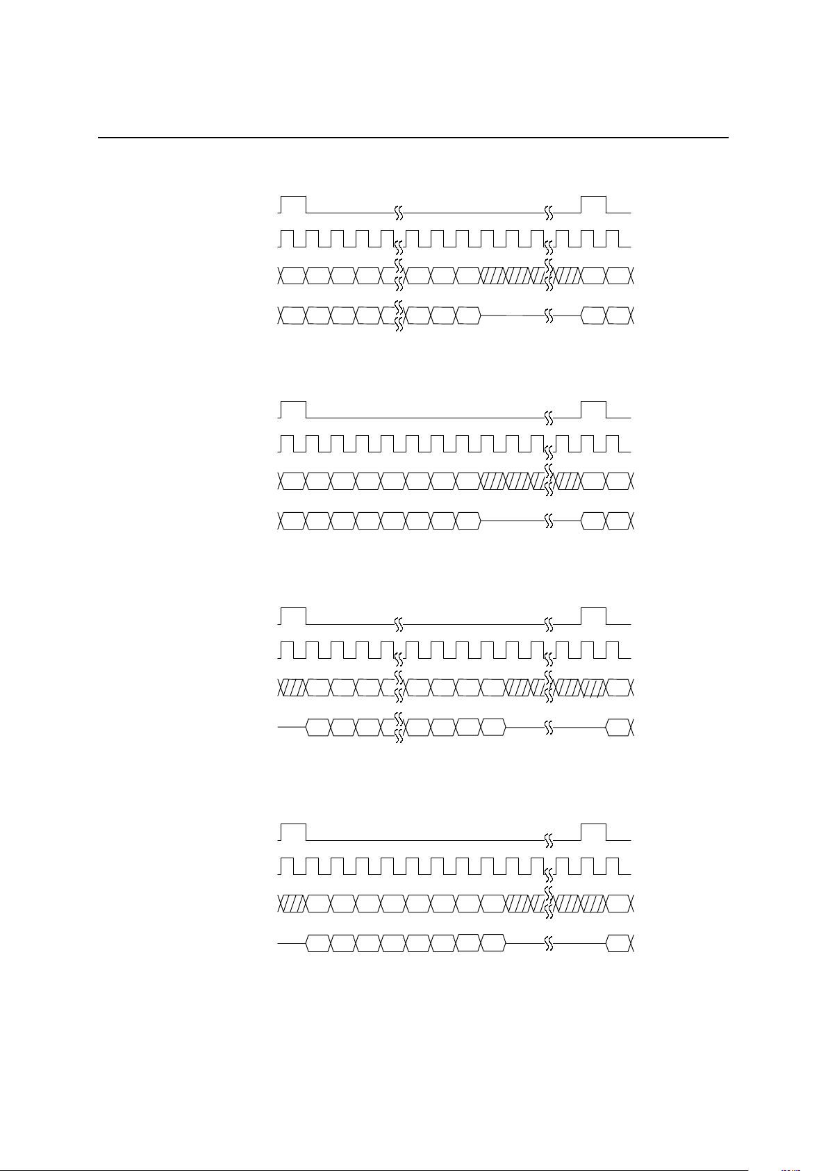
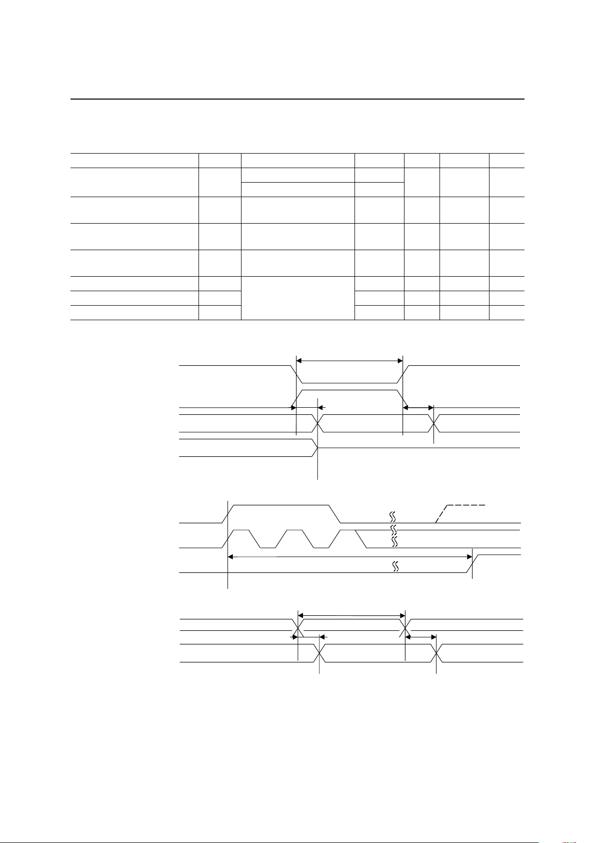
Figure 3 Digital Interface Timing
SYNC
(b) µ-law PCM coding format timing (normal sync)
BCLK
PCMI
PCMEI
PCMO
PCMEO
D7 D6 D5 D4 D3 D2 D1 D0 D7 D6
Hi-Z
D7 D6 D5 D4 D3 D2 D1 D0 D7 D6
SYNC
(a) 16-bit linear coding format timing (normal sync)
BCLK
PCMI
PCMEI
PCMO
PCMEO
D15 D14 D13 D12 D2 D1 D0 D15 D14
Hi-Z
D15 D14 D13 D12 D2 D1 D0 D15 D14
SYNC
(c) 16-bit linear coding format timing (short-frame sync)
BCLK
PCMI
PCMEI
PCMO
PCMEO
D15 D14 D13 D2 D1 D0 D15
D3
Hi-Z
D15 D14 D13 D2 D1 D0 D15
Hi-Z
D3
SYNC
(d) µ-law PCM coding format timing (short-frame sync)
BCLK
PCMI
PCMEI
PCMO
PCMEO
D7D7 D6 D5 D4 D3 D2 D1 D0
Hi-Z
D7D7 D6 D5 D4 D3 D2 D1 D0
Hi-Z
Page 9

FEDL7731-02-04
1
Semiconductor
MSM7731-02
9/53
ECSEL
This is the echo canceler mode selection pin. A logic “1” selects the single echo canceler mode and a logic “0”
selects the dual echo canceler mode. If the pin setting is changed, reset must be activated by either the
PDN/RST
pin or the PDN/RST bit (CR0-B7). If the single echo canceler mode is selected, echo canceler control on the
line-side is unnecessary. This pin is ORed with the CR0-B0 bit of the control register. Refer to the section
“RELATIONSHIP BETWEEN PINS AND CONTROL REGISTERS”.
LTHR/ATHR
This is the “through mode” control pin for the echo canceler. In the “through mode”, SinL/A and RinL/A data is
directly output to SoutL/A and RoutL/A res pectively while each respective echo coefficient is maintained. A logic
“0” selects the normal mode (echo canceler operation) and a logic “1” selects the “through mode”. In the through
mode, the functions of HD, HLD, ATT and GC are inv alid. Because data is shifted in to this pin in syn chronization
with the rising edge of the SYNC signal, hold the data at the pin for 250 µs or longer. This pin is ORed with the
CR4-B7 and CR5-B7 bits of the control register. Refer to the section “RELATIONSHIP BETW EEN PINS AND
CONTROL REGISTERS”.
LHD
LHDLHD
LHD/AHD
AHDAHD
AHD
This pin turns ON or OFF the function to detect and cancel the howling that occurs in an acoustic system such as a
handsfree communication system. A logic “0” turns the function ON and a logic “1” turns the function OFF. This
function is valid when the LTHR/ATHR pin is in the normal mode. Because data is shifted into this pin in
synchronization with the rising edge of the SYNC signal, hold the data at the pin for 250 µs or longer. This pin is
ORed with the CR4-B4 and CR4-B4 and CR5-B4 bits of the control register. Refer to the section
“RELATIONSHIP BETWEEN PINS AND CONTROL REGISTERS”.
LATT
LATTLATT
LATT
This pin turns ON or OFF the ATT function to prevent howling by means of attenuators (ATTsL, ATTrL)
provided in the RinL inputs and SoutL outputs of the echo canceler. A logic “0” turns ON and a logic “1” turns
OFF the ATT function. If input is only to RinL, the ATTsL for SoutL is activated. If input is only to SinL, or if
there is input to both SinL and RinL, the ATTrL for RinL input is activated. The ATT value of each attenuator is
approximately 6 dB. This function is valid w h en the LTHR pin is in the n ormal mode. Becaus e data is shifted into
this pin in synchronization with the rising edge of the SYNC signal, hold the data at the pin for 250 µs or longer.
This pin setting is logically ORed with the CR4-B1 bit of the control register. Refer to the section
“RELATIONSHIP BETWEEN PINS AND CONTROL REGISTERS”.
AATT
AATTAATT
AATT
This is the ATT atlenuation selection pin to prevent howling by means of attenuators (ATTsA, ATTrA) provided
in the RinA inputs and SoutA outputs of the ech o can celer. A logic “ 0” selects 6 dB and a log ic “1” selects 12 dB.
If input is only to RinA, the ATTsA for SoutA is activated. If input is only to SinA, or if there is input to both SinA
and RinA, the ATTrA for RinA input is activated. This function is valid when the ATHR pin is in the normal m ode.
Because data is shifted into this pin in synchronization with the ris ing edge of the SYNC signal, h old the data at the
pin for 250 µs or longer. This pin setting is logically ORed with the CR5-B1 bit of the control register. Refer to the
section “RELATIONSHIP BETWEEN PINS AND CONTROL REGISTERS”.
Page 10

FEDL7731-02-04
1
Semiconductor
MSM7731-02
10/53
LGC
LGCLGC
LGC/AGC
AGCAGC
AGC
This pin turns ON or OFF the gain control function to control the input level and prevent howling by means of gain
controls (GainL/A) provided in the RinL/A inputs of the echo canceler. The gain controller adjusts the RinL/A
input level when it is –10 dBm0 or above, and it has the control range of 0 to –8.5 dB. A logic “0” turns the
function ON and a logic “1” turns the function OFF. This functio n is valid when the LTHR/ATHR p in is in the
mormal mode. Because data is shifted into this pin in synchronization with the rising edge of the SYNC signal,
hold the data at the pin for 250 µs or longer. This pin is ORed with the CR4-B0 and CR5-B0 bits of the control
register. Refer to the section “RELATIONSHIP BETWEEN PINS AND CONTROL REGISTERS”.
Notes:
Lxx/Axx : In the above, Lxx refers to line echo canceler control pins and Axx to acoustic echo canceler control
pins.
xxL/xxA : In the above pin descriptions, xxL refers to line echo canceler functions and xxA to acoustic echo
canceler functions.
GLPADTHR
GLPADTHRGLPADTHR
GLPADTHR
This is the mode control pin for the attenuators (LPADL/A) provided in the SinL/A inputs and the amplifiers
(GPADL/A) provided in the SoutL/A outputs of the echo canceler. A logic “0” selects the “through mode” and a
logic “1” selects the normal m ode (PAD operation). The l evels are s et by t he CR10 regis ter. Settings of ± 18, ± 12,
± 6 and 0 dB are possible. The default setting is ± 12 dB. If the echo return loss (value of returned echo) is
amplified, set the LPAD level such that echo return loss will be attenuated. It is recommended to set the GPAD
level to the positive level equal to the LPAD level. If the pin se tting is changed, the coefficient reset must be
activated by either the
RST
pin or the RST bit (CR0-B6). Because data is shifted into this pin in synchronization
with the rising edge of the SYNC signal, hold the data at the pin for 250 µs or longer. This pin is ORed with the
CR1-B2 bit of the control register. Refer to the section “REL ATIONSHIP BET WEEN PINS AND CONTROL
REGISTERS”.
RST
RSTRST
RST
This input pin resets coefficients of the echo canceler and noise canceler. A logic “0” causes the reset state to be
entered. At this time, the filter coefficients for the echo canceler and noise canceler are reset. Control register
contents are preserved. While reset is being processed, there is not sound. During normal operation, set this pin to
a logic “1”. Use this pin in cases where the echo path changes (due to line switching during a telephone
conversation, etc.), or when resuming telephone communication. Because data is shifted into this pin in
synchronization with the rising edge of the SYNC signal, hold the data at the pin for 250 µs or longer. This pin is
ORed (negative logic) with the CR0-B6 bit of the control register. Refer to the section “RELATIONSHIP
BETWEEN PINS AND CONTROL REGISTERS”.
Page 11
FEDL7731-02-04
1
Semiconductor
MSM7731-02
11/53
NCSEL1, NCSEL2
These are the noise attenuation selection pins. In the “through mode” the noise canceler is halted and data is
directly output. In the “normal mode” the noise canceler operates normally. Since the noise attenuation in the
normal mode is selected after the initial mode has been released, the change of the noise attenuation during normal
operation is invalid. If the noise attenuation is changed, reset must be activated b y the
RDN/RST
pin or the
PDN/RST bit (CR0-B7). Changing t o the through mode during normal operati on and returning to the normal mode
are possible. The NCSEL1 pin is ORed with the CR1-B0 bit of the control register and the NCSEL2 pin is ORed
with the CR12-B2 bit of the control register. Refer to the section “RELATIONSHIP BETW EEN PINS AND
CONTROL REGISTERS”.
Note:
Since there is a trade-off between noise attenuation and sound quality after canceling the noise, select the noise
attenuation appropriate to the sound quality.
NCSEL2 NCSEL1 NC Mode Attenuation (dB) Quality
0 0 Normal Mode 17 Better
1 1 Normal Mode 13.5
1 0 Normal Mode 8 Best
0 1 Through Mode — —
NCPAD1, NCPAD2
These are the noise canceler I/O gain adjusting pins. The gain adjustment is valid for tone control after canceling
the noise. The bigger the input level of the noise canceler is, the better the sou nd quality is. T he NCPAD1 pin is
ORed with the CR4-B2 bit of the con trol register and th e NCPAD2 pin is OR ed w ith the CR5-B2 bit of the control
register. Refer to the section “RELATIONSHIP BETWEEN PINS AND CONTROL REGISTERS”.
NCPAD2 NCPAD1 GPADNC (dB) LPADNC (dB)
0000
016–6
1 0 12 –12
1 1 18 –18
DEN
DENDEN
DEN, EXCK, DIN, DOUT
This is the serial port for the microcontroller interface. 13 bytes of control registers are provided in this IC dev ice.
There pins are used to write and read data from an external microcontroller. The
DEN
pin is an enable signal input
pin, the EXCK pin is a clock signal inp ut pin for data shifting, t he DIN pin is an addr ess and data input pin, the
DOUT pin is a data output pin. If the mirrocontroller interface is not used, set the
DEN
pin to a logic “1” and the
EXCK and DIN pins to a logic “0”. In addition, use the MCUSEL pin to specify the “unused” setting of the
microcontroller interface. Figure 4 shows the input timing.
MCUSEL
This pin selects whether the microcontroller interface is used or unused. A logic “0” specifies that the
microcontroller interface is used and a logic “ 1” specifies that it is not used. If the microcontroller interface is not
used, this pin must be set to a logic “1”. This pin is ORed with the CR0-B1 bit of the control register. Refer to the
section “RELATIONSHIP BETWEEN PINS AND CONTROL REGISTERS”.
↔
Page 12
FEDL7731-02-04
1
Semiconductor
MSM7731-02
12/53
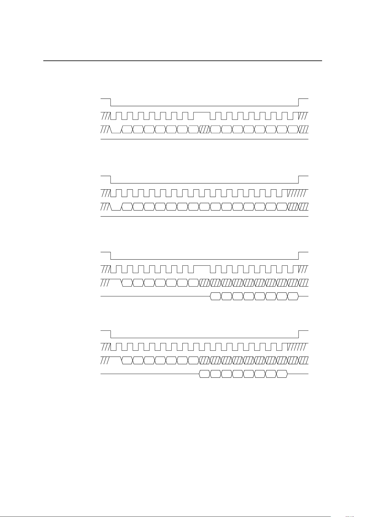
Figure 4 Microcontroller Interface I/O Timing
W A6A5A4A3A2A1A0 B7B6B5B4B3B2B1B0
12345678 910111213141516
DEN
EXCK
DIN
DOUT
(a) Data Write Timing 1 (8-bit MCU)
Hi-Z
W
A6 A5 A4 A3 A2 A1 A0 B7 B6 B5 B4 B3 B2 B1 B0
12345678910111213141516
(b) Data Write Timing 2 (16-bit MCU)
Hi-Z
DEN
EXCK
DIN
DOUT
R A6A5A4A3A2A1A0
B6 B5 B4 B3 B2 B1 B0B7
12345678 910111213141516
(c) Data Read Timing 1 (8-bit MCU)
Hi-Z Hi-Z
DEN
EXCK
DIN
DOUT
(d) Data Read Timing 2 (16-bit MCU)
123456789
10 11 12 13 14 15 16
R A6A5A4A3A2A1A0
B6 B5 B4 B3 B2 B1 B0B7
Hi-Z Hi-Z
DEN
EXCK
DIN
DOUT
Page 13
FEDL7731-02-04
1
Semiconductor
MSM7731-02
13/53
RPAD4, RPAD3, RPAD2, RPAD1
These are the receive signal gain adjusting and mute setting pins. Refer to Table 1 for the settings. Set these pins to
a logic “0” when controlling by the control register. Because data is shifted into this pin in synchronization with the
rising edge of the SYNC signal, hold the data at the pin for 250 µs or longer. For further details, refer to the
electrical characteristics. These pins are ORed with the CR2-B3, B2, B1 and B0 bits of th e con trol reg ister. R ef er
to the section “RELATIONSHIP BETWEEN PINS AND CONTROL REGISTERS”.
TPAD4, TPAD3, TPAD2, TPAD1
These are the transmit signal gain adjusting and mute setting pins. Refer to Table 1 for the settings. Set these pins
to a logic “0” when controlling by the control register. Becau se data is shifted into this pin in synchronization w ith
the rising edge of the SYNC signal, hold the data at the pin for 250 µs or longer. For further details, refer to the
electrical characteristics. These pins are ORed with the CR3-B3, B2, B1 and B0 bits of th e con trol reg ister. R ef er
to the section “RELATIONSHIP BETWEEN PINS AND CONTROL REGISTERS”.
Table 1 RPAD/TPAD Setting
RPAD4 RPAD3 RPAD2 RPAD1 TPAD4 TPAD3 TPAD2 TPAD1 Level
0111 011121 dB
0110 011018 dB
0101 010115 dB
0100 010012 dB
0011 00119 dB
0010 00106 dB
0001 00013 dB
0000 00000 dB
1111 1111–3 dB
1110 1110–6 dB
1101 1101–9 dB
1100 1100–12 dB
1011 1011–15 dB
1010 1010–18 dB
1001 1001–21 dB
1000 1000MUTE
TEST1-4
Test inputs. Set these pins to a logic “0”.
TEST9
Test output.
Page 14
FEDL7731-02-04
1
Semiconductor
MSM7731-02
14/53
ABSOLUTE MAXIMUM RATINGS
Parameter Symbol Condition Rating Unit
Power Supply Voltage V
DD
— –0.3 to +5.0 V
Digital Input Voltage V
IN
— –0.3 to VDD+0.3 V
Digital output Voltage V
OUT
— –0.3 to VDD+0.3 V
Storage Temperature T
STG
— –55 to +150 °C
RECOMMENDED OPERATING CONDITION
Parameter Symbol Condition Min. Typ. Max. Unit
Power Supply Voltage V
DD
— 2.7 — 3.6 V
Operating Temperature T
a
— –40 +25 +85 °C
SYNC, BCLK input pins 0.5×V
DD
MCK/X1 input pin 0.65×V
DD
Input High Voltage V
IH
Other digital input pins 0.45×V
DD
—VDDV
MCK/X1 input pin 0.35×V
DD
Input Low Voltage V
IL
Other digital input pins
0—
0.16×V
DD
V
Digital Input Rise Time t
IR
All digital inputs — — 20 ns
Digital Input Fall Time t
If
All digital inputs — — 20 ns
Master Clock Frequency f
MCK
MCK/X1 –100 ppm +19.2 +100 ppm MHz
Master Clock Duty Ratio D
MCK
MCK/X1 40 50 60 %
Bit Clock Frequency f
BCK
BCLK (during output) 64 — 2048 kHz
Bit Clock Duty Ratio D
CK
BCLK (during output) 40 50 60 %
Synchronous Signal
Frequency
f
SYNC
SYNC (during output) –100 ppm 8 +100 ppm kHz
Synchronous Signal Width t
WS
SYNC (during output) 1 BCLK — 100 ns
t
BS
BCLK to SYNC
(during input)
100 — — ns
Transmit/Receive Sync
Signal Setting Time
t
SB
SYNC to BCLK
(during input)
100 — — ns
R
DL
DOUT, PCMO, PCMEO 1 — — k
Ω
C
DL1
DOUT, PCMO, PCMEO — — 50 pF
Digital Output Load
C
DL2
SYNC, BCLK
(during output)
— — 20 pF
Bypass Condenser for SG C
SG
SG to AG 10+0.1 — — µF
Page 15
FEDL7731-02-04
1
Semiconductor
MSM7731-02
15/53
ELECTRICAL CHARACTERISTICS
DC Characteristics
(VDD = 2.7 to 3.6 V, Ta = –25 to +85°C)
Parameter Symbol Condition Min. Typ. Max. Unit
Power Supply Current 1 I
DD1
Operating, no signal
(V
DD
= 3.0 V)
—3550mA
Power Supply Current 2 I
DD2
Power down mode
(V
DD
= 3.0 V, MCK = 0 V)
—0.02 1 mA
I
IH
VI = V
DD
—— 2 µA
Input Leakage Current
I
IL
VI = 0 V — — 2 µA
High Level Digital Output
Voltage
V
OH
IOH = 0.4 mA
(other than ×2)
0.5×V
DD
—VDDV
Low Level Digital Output
Voltage
V
OL
IOL = 3.2 mA
(other than ×2)
—0 0.2 0.4 V
Digital Output Leakage
Current
I
O
DOUT, PCMO, PCMEO — — 10 µA
Input Capacitance C
IN
——5—pF
Analog Interface Characteristics
(VDD = 2.7 to 3.6 V, Ta = –25 to +85°C)
Parameter Symbol Condition Min. Typ. Max. Unit
R
INA
AIN, APWI 10 — — M
Ω
Input Resistance
R
INL
LIN, LPWI 10 — — M
Ω
R
LA1
AGSX, AVFRO 20 — — k
Ω
R
LA2
AOUT 1.2 — — k
Ω
R
LL1
LGSX, LVFRO 20 — — k
Ω
Output Load Resistance
R
LL2
LOUT 1.2 — — k
Ω
C
LA1
AGSX, AVFRO, AOUT — — 100 pF
Output Load Capacitance
C
LL1
LGSX, LVFRO, LOUT — — 100 pF
V
OA1
AGSX,
AVFRO
R
L
= 20 k
Ω
——1.3Vpp
V
OA2
AOUT RL = 1.2 k
Ω
——2.6Vpp
V
OL1
LGSX,
LVFRO
R
L
= 20 k
Ω
——1.3Vpp
Output Voltage Level (*1)
V
OL2
LOUT RL = 1.2 k
Ω
——2.6Vpp
V
OFA1
AVFRO –100 — +100 mV
V
OFA2
AOUT –20 — +20 mV
V
OFL1
LVFRO –100 — +100 mV
Offset Voltage
V
OFL2
LOUT –20 — +20 mV
SG Output Voltage V
SG
SG — 1.4 — V
SG Output Impedance R
SG
SG — 40 80 k
Ω
Note*1: 0.320 Vrms = 0 dBm0, +3.14 dBm0 = 1.30 V
PP
Page 16
FEDL7731-02-04
1
Semiconductor
MSM7731-02
16/53
Digital Interface Characteristics (1/3)
(VDD = 2.7 to 3.6 V, Ta = –25 to +85°C)
Parameter Symbol Condition Min. Typ. Max. Unit
PDN/RST
pin 1
Power-down/Reset Signal
Pulse Width
t
RSTW
PDN/RST control bit 1.6
——µS
Power-down/Reset Start
Time
t
PDND
PDN/RST
pin and
PDN/RST control bit
— — 50 nS
Power down/Reset End Time t
PDNH
PDN/RST
pin and
PDN/RST control bit
— — 200+
α
mS
Power-down/Reset Internal
Setting Time
t
PDNS
SYNC pin (input mode) 140 — 180 µS
Control Pulse Width t
PARW
250 — — µS
Control Start Time t
PARD
— — 250 µS
Control End Time t
PARH
(*2)
— — 250 µS
α
: Crystal activation
PDN/RST Timing
PDN/RST set timing
Control Timing (*2)
Note*2: Applies to the following pins/control bits:
LINEEN
, SLPTHR, NCTHR,
GLPADTHR
, TPAD6-1, RPAD6-1,
RST
, ATHR,
AATT
, AHLD,
AHD, AGC
, LTHR,
LATT
, LHLD,
LHD, LGC
pins, and control bits.
Power Down
Initial Mode
Hi-Z
t
PDND
t
PDNH
T
RSTW
PDN/RST
pin
PDN/RST control bi
t
Internal Operation
PCMO, PCMEO
SYNC (Ext. clock)
BCLK (Ext. clock)
PDN/RST control bit
(
Internal Write
)
t
PDNS
Internal processing
t
PARD
t
PARH
t
PARW
Pin/control bit
Internal operation
Page 17

FEDL7731-02-04
1
Semiconductor
MSM7731-02
17/53
Digital Interface Characteristics (2/3)
(VDD = 2.7 to 3.6 V, Ta = –25 to +85°C)
Parameter Symbol Condition Min. Typ. Max. Unit
CDL = 20 pF
(output mode, PCM)
—64 —kHz
Bit Clock Frequency f
BCK
CDL = 20 pF
(output mode, linear)
— 128 — kHz
Bit Clock Duty Ratio D
CK
CDL = 20 pF (output mode) 40 50 60 %
Sync signal frequency f
SYNC
CDL = 20 pF (output mode) — 8 — kHz
Sync signal Duty Ratio D
SYNC
CDL = 20 pF (output mode) 40 50 60 %
t
BS
BCLK to SYNC
(output mode)
100 — — ns
Transmit/Receive Sync
Signal Setting Time
t
SB
SYNC to BCLK
(output mode)
100 — — ns
Input Setup Time t
DS
— 100 — — ns
Input Hold Time t
DH
— 100 — — ns
t
SDX
RDL = 1 kΩ, CDL = 50 pF — — 100 ns
Digital Output Delay Time
t
XD1
RDL = 1 kΩ, CDL = 50 pF — — 100 ns
t
XD2
RDL = 1 kΩ, CDL = 50 pF — — 100 ns
Digital Output Hold Time
t
XD3
RDL = 1 kΩ, CDL = 50 pF — — 100 ns
Digital Input Timing (Normal-sync)
Digital Input Timing (Short-frame-sync)
BCLK
SYNC
PCMI
PCMEI
1
0 2345678910
MSB
LSB
t
BS
t
SB
t
WS
t
DS
t
DH
BCLK
SYNC
PCMI
PCMEI
1
0 2345678910
MSB LSB
t
BS
t
SB
t
WS
t
DS
t
DH
Page 18

FEDL7731-02-04
1
Semiconductor
MSM7731-02
18/53
Digital Output Timing (Normal-sync)
Digital Output Timing (Short-frame-sync)
Digital Interface Characteristics (3/3)
(VDD = 2.7 to 3.6 V, Ta = –25 to +85°C)
Parameter Symbol Condition Min. Typ. Max. Unit
t
M1
—20——ns
t
M2
—20——ns
t
M3
—50——ns
t
M4
— 100 — — ns
t
M5
—50——ns
t
M6
—50——ns
t
M7
RD = 1 kΩ, CDL = 20 pF — — 30 ns
t
M8
RD = 1 kΩ, CDL = 20 pF 0 — — ns
t
M9
—50——ns
t
M10
RD = 1 kΩ, CDL = 20 pF — — 30 ns
MCU Interface Digital
Input/Output Setting Time
t
M11
— 100 — — ns
EXCK Clock Frequency f
EXCK
———10MHz
BCLK
SYNC
PCMO
PCMEO
1
0 2345678910
MSB LSB
t
BS
t
SB
t
WS
t
SDX
t
XD1
t
XD2
Hi-Z Hi-Z
t
XD3
BCLK
SYNC
PCMO
PCMEO
1
0 2345678910
t
BS
t
SB
t
WS
MSB
LSB
t
XD2
Hi-Z
Hi-Z
t
XD3
t
XD1
Page 19

FEDL7731-02-04
1
Semiconductor
MSM7731-02
19/53
Microcontroller Interface I/O Timing
DEN
EXCK
DIN
DOUT
t
M1
t
M2
t
M3
t
M4
t
M5
t
M6
t
M7
t
M8
t
M10
t
M11
t
M9
12345678910111213141516
W/RA6A5A4A3A2A1A0B7B6B5B4B3B2B1B0
B7 B6 B5
B4 B3 B2 B1 B0
Page 20

FEDL7731-02-04
1
Semiconductor
MSM7731-02
20/53
AC Characteristic (Line side CODEC/Acoustic side CODEC)
(VDD = 2.7 to 3.6 V, Ta = –40 to +85°C)
Condition
Parameter Symbol
Freq. (Hz)
Level
(dBm0)
Others
Min. Typ. Max. Unit
L
OSS
T1 0 to 60 25 — —
L
OSS
T2 300 to 3000 –0.15 — +0.20
L
OSS
T3 1020 Reference
L
OSS
T4 3300 –0.15 — +0.80
L
OSS
T5 3400 0 — 0.80
Transmit Frequency
Response
L
OSS
T6 3968.75
0(*3)
13 — —
dB
L
OSS
R1 0 to 3000 –0.15 — +0.20
L
OSS
R2 1020 Reference
L
OSS
R3 3300 –0.15 — +0.80
L
OSS
R4 3400 0 — 0.80
Receive Frequency
Response
L
OSS
R5 3968.75
0(*3)
13 — —
dB
SD T1 3 35 — —
SD T2 0 35 — —
SD T3 –30 35 — —
SD T4 –40 28 — —
Transmit Signal to
Distortion Ratio
SD T5
1020
–45
(*3, *4)
23 — —
dB
SD R1 3 35 — —
SD R2 0 35 — —
SD R3 –30 35 — —
SD R4 –40 28 — —
Receive Signal to
Distortion Ratio
SD R5
1020
–45
(*3, *4)
23 — —
dB
GT T1 3 –0.2 — +0.2
GT T2 –10 Reference
GT T3 –40 –0.2 — +0.2
GT T4 –50 –0.5 — +0.5
Transmit Gain
Tracking
GT T5
1020
–55
(*3)
–1.2 — +1.2
dB
GT R1 3 –0.2 — +0.2
GT R2 –10 Reference
GT R3 –40 –0.2 — +0.2
GT R4 –50 –0.5 — +0.5
Receive Gain
Tracking
GT R5
1020
–55
(*3)
–1.2 — +1.2
dB
N
IDLT
——(*3, *4)——
–68
(–75.7)
Idle Channel Noise
N
IDLR
——(*3, *4)——
–72
(–79.7)
dBm0p
(dBmp)
A
VT
A/LGSX (*3) 0.285 0.32 0.359 Vrms
Absolute Signal
Amplitude
A
VR
1020 0
A/LVFRO
(*3)
0.285 0.32 0.359 Vrms
P
SRRT
30 — — dB
Power Supply Noise
Rejection Ratio
P
SRRR
Noise Freq:
0 to 50 kHz
Noise
Level:
50 mV
PP
(*3)
30 — — dB
Note: *3. CODEC input/output gain = 1
*4. P-message weighted filter used
0.320 Vrms = 0 dBm0 = –7.7 dBm
Page 21

FEDL7731-02-04
1
Semiconductor
MSM7731-02
21/53
Noise Canceler Characteristics
(VDD = 2.7 to 3.6 V, Ta = –40 to +85°C)
Parameter Symbol Condition Min. Typ. Max. Unit
Noise Attenuation N
res
White Noise, voice band 13 17 — dB
Measurement System Block Diagram
Echo Canceler Characteristics
(VDD = 2.7 to 3.6 V, Ta = –40 to +85°C)
Parameter Symbol Condition Min. Typ. Max. Unit
Acoustic
Line side (when CODEC or 16-bit
linear data interface is used)
35
Echo Attenuation E
res
Line side (µ-law PCM used)
—
30
—dB
T
acoud
Single mode — — 59 mS
T
acoud
Dual mode (acoustic side) — — 59–T
lined
mS
Cancelable Echo
Delay Time
T
lined
Dual mode (line side) — — 27 mS
Measurement System Block Diagram
L.P.F.
5 kHz
Analog
AIN
NC
LOUT
Analog
Level meter
MSM7731-02
Power supply voltage 3 V
CODEC input gain = 1
CODEC output gain = 1
White noise generator
L.P.F.
5 kHz
Analog
RIN ROUT
Analog
Delay
MSM7731-02
Power supply voltage 3 V
CODEC input gain = 1
CODEC output gain = 1
White noise generator
Line or Acoustic
EC
SOUT
SIN
Analog
Analog
Level meter
ATT
E.R.L
(echo return loss)
Echo delay time
T
D
Page 22

FEDL7731-02-04
1
Semiconductor
MSM7731-02
22/53
Rin input level vs. echo attenuation
(Measuring Co nd iti on s) Rin signal : 5 kHz band white noise
E.R.L : –6 dB
Delay time : 4 ms
ATT, GC : OFF
Noise floor : –60 dBm (P-message filter unused)
E.R.L level vs. echo attenuation (with GLPAD)
(Measuring Condition) Rin si gnal : 5 kHz band white noise
Rin input level : –20 dBm (with GLPAD = ±0 dB)
: –26 dBm (with GLPAD = ±6 dB)
: –32 dBm (with GLPAD = ±12 dB)
: –38 dBm (with GLPAD = ±18 dB)
Delay time : 4 mS
ATT, GC : OFF
Noise floor : –60 dBm (P-message filter unused)
E.R.L vs. echo attenuation (with GLPAD)
45
Echo attenuation [dB]
40
35
30
25
20
15
10
5
0
E.R.L [dB]
-40
0 5 10 15 20 25
GLPAD=±0dB
GLPAD=±6dB
GLPAD=±12dB
GLPAD=±18dB
-35 -30 -25 -20 -15 -10 -5
RIN input level vs. echo attenuation
0
5
10
15
20
25
30
35
40
45
-50
Rin input level [dBm]
Echo attenuation [dB]
-45 -40 -35 -30 -25 -20 -15 -10
Page 23

FEDL7731-02-04
1
Semiconductor
MSM7731-02
23/53
Echo delay time vs. echo attenuation (Dual echo canceler mode/acoustic side)
(Measuring Condition) Rin si gnal : 5 kHz band white noise
Rin input level : –16 dBm
E.R.L : –6 dB
ATT, GC : OFF
Noise floor : –60 dBm (P-message filter unused)
Echo delay time vs. echo attenuation (Dual echo canceler mode/line side)
(Measuring Condition) Rin si gnal : 5 kHz band white noise
Rin input level : –16 dBm
E.R.L : –6 dB
ATT, GC : OFF
Noise floor : –60 dBm (P-message filter unused)
Echo delay time vs. echo attenuation
Dual echo canceler mode (acous t ic side)
0
5
10
15
20
25
30
35
40
45
5 1015202530354045505560
Echo delay time [ms]
Echo attenuation [dB]
Echo delay time vs. echo attenuation
5 1015202530354045505560
Echo delay time [ms]
0
5
10
15
20
25
30
35
40
45
Echo attenuation [dB]
Dual echo canceler mode (lin e si de)
Page 24

FEDL7731-02-04
1
Semiconductor
MSM7731-02
24/53
Echo delay time vs. echo attenuation (Single echo canceler mode)
(Measuring Condition) Rin si gnal : 5 kHz band white noise
Rin input level : –16 dBm
E.R.L : –6 dB
ATT, GC : OFF
Noise floor : –60 dBm (P-message filter unused)
Slope filter frequency characteristic (with CODEC filter frequency characteristic)
(Measuring Condition) Rin input level : –16 dBm
Noise floor : –60 dBm (P-message filter unused)
Echo delay time vs. echo attenuation
Single echo canceler mode
0
5
10
15
20
25
30
35
40
45
5 1015202530354045505560
Echo delay time [ms]
Echo attenuation [dB]
Slope filter frequency characteristic
0
10
-10
-20
-30
-40
-50
-60
10015011 1501 2001 2501 3001
3501
Frequency [ms]
Gain [ dB]
Page 25

FEDL7731-02-04
1
Semiconductor
MSM7731-02
25/53
Echo Canceler Characteristics Data 1 (Line Echo, White Noise)
(Measuring Condition) Rin si gnal : 5 kHz band white noise
Rin input level : –20 dBm
E.R.L : 0 dB
ATT, GC : OFF
Noise floor : –60 dBm (P-message filter unused)
Echo attenuation = 40 dB
Echo Canceler Characteristics Data 2 (Line Echo, Voice)
(Measuring Condition) Rin si gnal : voice
Rin input level : about –20 dBm
E.R.L : 0 dB
ATT, GC : OFF
Noise floor : –60 dBm (P-message filter unused)
Echo attenuation = 34 dB
Echo Canceler Characteristics Data 3 (Acoustic echo, Voice)
(Measuring Condition) Rin si gnal : voice
Rin input level : about –20 dBm
Speaker output level : 80 dB (A) (at 1 m)
Distance from microphone and speaker : 5 cm
GC : OFF
ATT, Noise Canceler : OFF
Noise floor : –60 dBm (P-message filter unused)
Echo attenuation = 34 dB
Measurement System Block Diagram (Acoustic Echo)
3 V
+
R9
22 k
MIC
C10
1 µ
AGSX
AIN
AVFRO
APWI
AOUT
AG
SP
R13
22 k
R14
22 k
R15
1.2 k
RV4
10 k
RV1
0.734 k
R8
2.2 k
C9
10 µ
R7
100
J1
MIC
C13
0.1
µ
R16
10 k
1
2
3
4
8
7
6
5
R17
470 k
C15
10
p
AG
5 V
J3
SP
C14
0.1 µ
M7731
EC
SOUT SIN
ROUTRIN
U13LM4861
Page 26

FEDL7731-02-04
1
Semiconductor
MSM7731-02
26/53
FUNCTIONAL DESCRIPTION
Control Registers
Table 2 Control Register Map
Address Contents
A6 A5 A4 A3 A2 A1 A0 B7 B6 B5 B4 B3 B2 B1 B0
R/W
CR0 0 0 0 0 0 0 0 *PDN/RST *RST *#
LINEEN#CLKEN#PCMEN#PCMEEN
OPE
*#MCUSEL
OPE
*#ECSEL
R/W
CR1 0 0 0 0 0 0 1 #DMW R — — — — *
GLPADTHR
*SLPTHR *#NCSEL1 R/W
CR2 0 0 0 0 0 1 0 — — RPAD6 RPAD5 *RPAD4 *RPAD3 *RPAD2 *RPAD1 R/W
CR3 0 0 0 0 0 1 1 — — TPAD6 TPAD5 *TPAD4 *TPAD3 *TPAD2 *TPAD1 R/W
CR4 0 0 0 0 1 0 0 *LTHR — LHLD *
LHD
LCLP *NCPAD1 *
LATT
*
LGC
R/W
CR5 0 0 0 0 1 0 1 *ATHR — AHLD *
AHD
ACLP *NCPAD2 *
AATT
*
AGC
R/W
CR6 0 0 0 0 1 1 0 A15 A14 A13 A12 A11 A10 A9 A8 R/W
CR70000111A7A6A5A4A3A2A1A0R/W
CR8 0 0 0 1 0 0 0 D15 D14 D13 D12 D11 D10 D9 D8 R/W
CR90001001 D7 D6 D5 D4 D3 D2 D1 D0 R/W
CR10 0 0 0 1 0 1 0 GPADA2 GPADA1 LPADA2 LPADA1 GPADL2 GPADL1 LPADL2 LPADL1 R/W
CR11 0 0 0 1 0 1 1 READY — — — — — *#PCMSEL #SYPDN R/W
CR12 0 0 0 1 1 0 0 — — — — — *#NCSEL2 — — R/W
Note * : Shared control bits with port (pin)
– : Reserved bits. Do not change the initial value (“0”).
# : Control bit that can be changed only in the initial mode.
Reg
Name
Page 27

FEDL7731-02-04
1
Semiconductor
MSM7731-02
27/53
(1) CR0 (basic operating mode setting)
B7 B6 B5 B4 B3 B2 B1 B0
CR0 PDN/RST RST
LINEEN CLKEN PCMEN PMCEEN
OPE
MCUSEL
OPE
ECSEL
Initial
Value (*5)
00000000
Note*5: Initial values are the values set when reset is activated by the
PDN/RST
pin. (Initial values are
also set in the same manner, except for CR0-B7, when reset by the PDN/RST bit of B7.)
B7 Power-down and Reset 0: power-on 1: power-down reset
During power-down reset, this device enters the power-down state. At this time all control register bits,
internal variables, and the coefficients for the echo canceler and noise canceler are reset. After powerdown reset is released, this device enters the initial mode. This bit is internally ORed with the inverted
PDN/RST
signal. Refer to the section “RELATIONSHIP BETWEEN PINS AND CONTROL
REGISTERS”.
B6 Reset control 0: normal operation 1: reset
At reset, the coefficients for the echo canceler and noise canceler and noise canceler are reset. Control
register contents preserved. While reset is being processed, there is no sound. Use this bit in cases where
the echo path changes (due to line switching during a telephone conversation, etc.), or when resuming
telephone communication. Because data is read by this bit in synchronization with the rising edge of the
SYNC signal, hold the data in the bit for 250 µs or longer. This bit is internally ORed with the inverted
RST
signal. Refer to the section “RELATIONSHIP BETWEEN PINS AND CONTROL
REGISTERS”.
B5 Line CODEC power-down control 0: normal operation 1: power-down
During power-down, the line CODEC is in the power- down state, th e line CODEC output pin is at high
impedance and line CODEC input pin is internally processed as an idle pattern input. This bit is
internally ORed with the
LINEEN
pin. When the line CODEC is not used, this control results in low
consumption of electrical power. This bit can only be set to “0” or “1” during power-down reset and
initial mode. Refer to the section “RELATIONSHIP BETWEEN PINS AND CONTROL
REGISTERS”.
B4 SYNC, BCLK output control 0: ON 1: OFF
When OFF, the SYNC and BCLK output pins are in the high impedance state. This control is valid
when the CLKSEL pin is at a logic “0” and has selected the internal clock mode. When the SYNC and
BCLK clocks are not used externally, this control results in low consumption of electrical power.
This bit can only be set to "0" or "1" during power-down reset and the initial mode.
B3 PCMI/O control 0:ON 1: OFF
When OFF, the PCMO output pin is in the high impedance state and the PCMI input pin is internally
processed as an idle pattern input. When the line digital interface is not used, this control results in low
consumption of electrical power.
This bit can only be set to "0" or "1" during power-down reset and the initial mode.
B2 PCMEI/O control 0:ON 1: OFF
When OFF, the PCMEO output pin is in the high im pedance state and the PC MEI input pin is intern ally
processed as an idle pattern input. When the line digital interface is not used, this control results in low
consumption of electrical power.
This bit can only be set to "0" or "1" during power-down reset and the initial mode.
Page 28

FEDL7731-02-04
1
Semiconductor
MSM7731-02
28/53
B1, B0 Operation mode selection
(0, 0): Initial mode
Approximately 200 ms after power-down reset is released, the initial mode is entered.
Only in this mode can the contents of the internal default value store memory be modified and CR0-B5
to CR0-B0, CR1-B7, CR1-B0, CR11-B1, CR11-B0, and CR12-B2 be set. In this mode, digital signal
output pins are at high impedance, digital communication input pins are internally processed as idle
pattern inputs, and neither the echo canceler nor the noise canceler operates. This m ode is skipped when
the MCUSEL pin is a logic “1”. This mode is released by setting the modes shown below. Refer to the
flow chart of Figure 5.
(1, 0): Dual echo canceler mode
The acoustic echo canceler, line echo canceler and other functions can be operated by control from the
control regi st ers. Refer to Figure 6.
The initial setting for cancelable echo delay time is as follows:
Acoustic delay time = 44 ms
Line delay time = 15 ms
(1, 1): Single echo canceler mode
The acoustic echo canceler and other functions can be operated by control from the control registers.
Control of the line echo canceler is unnecessary in this mode .Refer to Figure 7.
The initial setting for cancelable echo delay time is as follows:
Acoustic delay time = 59 ms
(Other): Reserved bit (cannot be used)
Note: The MCUSEL pin is internally ORed with B1, and the ECSEL pin is internally ORed with B0. To
return to the initial mode after it has been released, activate power-down reset.
Automatic setting
Acoustic
CODEC
Acoustic
Echo
Canceler
Line
CODEC
Noise
Canceler
Slope
Filter
Figure 7 Single Echo Canceler Mode
Acoustic
CODEC
Acoustic
Echo
Canceler
Line
CODEC
Noise
Canceler
Slope
Filter
Line
Echo
Canceler
Figure 6 Dual Echo Canceler Mode
Automatic setting
PDN/RST
PDN/RST release
Set control register
READY(CR11-B7) = 1
Modify default store memory
CR0-B1=1
Start Normal Operation
Power-down state
YES
NO
Wait for 200 ms
∙ Control registers are reset.
∙ Internal variables are reset.
Initial Mode
Figure 5 Initial Mode Flowchart
READY(CR11-B7) = 0
Page 29

FEDL7731-02-04
1
Semiconductor
MSM7731-02
29/53
(2) CR1
B7 B6 B5 B4 B3 B2 B1 B0
CR1 DMWR — — — —
GLPADTHR
SLPTHR NCSEL1
Initial Value 0 0 0 0 0 0 0 0
B7 Internal data memory write control 0: write inhibited 1: write
In internal data memory, the data set in CR8 (D15 to D8) and CR9 (D7 to D0) is written to the memory
address set in CR6 (A15 to A8) and CR7 (A7 to A0).
Writing is possible only during the initial mode.
For further details, refer to the internal data memory access method.
B6, B5, B4, B3 Reserved bits. Modification of initial values is inhibited.
B2 Echo Canceler I/O P AD control 0: “through mode” 1: normal mode
This bit controls the attenuators (LPADL/A) provided in the SinL/A inputs and the amplifiers
(GPADL/A) provided in the SoutL/A outputs of the echo canceler. Levels are set by the CR10 reg is ter,
and ±18, ±12, ±6 and 0 dB can be set. The defau lt value is ±12 dB . Use t his bit w hen the echo return loss
(value of returned echo) is amplified. If the pin setting is changed, the coefficient reset must be activated
by either the
RST
pin or the RST bit (CR0-B6). Because data is read by this bit in synchronization with
the rising edge of the SYNC signal, hold the data in the bit for 250 µs or longer. This bit is internall y
ORed with the
GLPADTHR
pin.
B1 Slope filter control 0: normal mode (slope filter operation) 1: “through mode”
This bit controls operation of the transmit slope filter. In the “through mode”, the filter is halted and data
is output directly. The slope filter decreases noises of low frequencies and improves the speech quality.
Refer to the frequency characteristics of slope filter. Because data is read by this bit in synchronization
with the rising edge of the SYNC signal, hold the data in the bit for 250 µs or longer. This bit is
internally ORed with the SLPTHR pin.
B0 Noise attenuation selection control 0: normal mode 1: “through mode”
This bit selects the noise attenuation of the noise canceler. In the “through mode”, the noise canceler is
halted and data is output directly. In the “ n ormal m ode” the n oise can celer operates n ormally . Since the
noise attenuation in the normal mode is selected after the initial mode has been released, the change of
the noise attenuation during normal operation is invalid. If the noise attenuation is changed, reset must
be activated by the
RDN/RST
pin or the PDN/RS T bit (CR 0-B7). Chan ging to the throug h mode during
normal operation and returning to the normal mode are possible. This bit is internally ORed with
NCSEL1 pin. (Refer to the NCSEL2 pin of CR12-B2.)
Note: Since there is a trade-off between noise attenuation and sound quality after canceling the noise, select
the noise attenuation appropriate to the sound quality.
NCSEL2 NCSEL1 NC Mode Attenuation (dB) Quality
0 0 Normal Mode 17 Better
1 1 Normal Mode 13.5
1 0 Normal Mode 8 Best
0 1 Through Mode — —
↔
Page 30

FEDL7731-02-04
1
Semiconductor
MSM7731-02
30/53
(3) CR2 (Receive side level control)
B7 B6 B5 B4 B3 B2 B1 B0
CR2 — — RPAD6 RPAD5 RPAD4 RPAD3 RPAD2 RPAD1
Initial Value 0 0 0 0 0 0 0 0
B7, B6 Reserved bit. Modification of initial values is inhibited.
B5, B4, B3, B2, B1,B0 Receive side level setting (RPAD)
These bits adjust the receive signal gain and set the mute level. Notice that only the mute level setting
differs from pin control. Because data is read by these bits in synchronization with the rising edge of the
SYNC signal, hold the data in these bits for 250 µs or longer.
When using this register, set the TPAD, 3, 2, 1 pins to a logic “0”.
(0, 0, 1, 0, 1, 0): 30 dB
(0, 0, 1, 0, 0, 1): 27 dB
(0, 0, 1, 0, 0, 0): 24 dB
(0, 0, 0, 1, 1, 1): 21 dB
(0, 0, 0, 1, 1, 0): 18 dB
(0, 0, 0, 1, 0, 1): 15 dB
(0, 0, 0, 1, 0, 0): 12 dB
(0, 0, 0, 0, 1, 1): 9 dB
(0, 0, 0, 0, 1, 0): 6 dB
(0, 0, 0, 0, 0, 1): 3 dB
(0, 0, 0, 0, 0, 0): 0 dB
(1, 1, 1, 1, 1, 1): –3 dB
(1, 1, 1, 1, 1, 0): –6 dB
(1, 1, 1, 1, 0, 1): –9 dB
(1, 1, 1, 1, 0, 0): –12 dB
(1, 1, 1, 0, 1, 1): –15 dB
(1, 1, 1, 0, 1, 0): –18 dB
(1, 1, 1, 0, 0, 1): –21 dB
(1, 1, 1, 0, 0, 0): –24 dB
(1, 1, 0, 1, 1, 1): –27 dB
(1, 1, 0, 1, 1, 0): –30 dB
(1, 1, 0, 1, 0, 1): –33 dB
(1, 1, 0, 1, 0, 0): –36 dB
(1, 1, 0, 0, 1, 1): –39 dB
(1, 1, 0, 0, 1, 0): –42 dB
(1, 1, 0, 0, 0, 1): –45 dB
(1, 1, 0, 0, 0, 0): –48 dB
(1, 0, 1, 1, 1, 1): –51 dB
(1, 0, 1, 1, 1, 0): –54 dB
(1, 0, 1, 1, 0, 1): –57 dB
(1, 0, 1, 1, 0, 0): –60 dB
(1, 0, 1, 0, 1, 1): MUTE
Page 31

FEDL7731-02-04
1
Semiconductor
MSM7731-02
31/53
(4) CR3 (Transmit Gain Adjustment)
B7 B6 B5 B4 B3 B2 B1 B0
CR3 — — TPAD6 TPAD5 TPAD4 TPAD3 TPAD2 TPAD1
Initial Value 0 0 0 0 0 0 0 0
B7, B6 Reserved bits. Modification of initial values is inhibited.
B5, B4, B3, B2, B1, B0 Transmit side level setting (TPAD)
These bits adjust the transmit signal gain and set the mute level. Notice that only the mute level setting
differs from pin control. Because data is read by these bits in synchronization with the rising edge of the
SYNC signal, hold the data in these bits for 250 µs or longer.
When using this register, set the TP AD4, 3, 2, 1 pins to a logic “0”.
(0, 0, 1, 0, 1, 0): 30 dB
(0, 0, 1, 0, 0, 1): 27 dB
(0, 0, 1, 0, 0, 0): 24 dB
(0, 0, 0, 1, 1, 1): 21 dB
(0, 0, 0, 1, 1, 0): 18 dB
(0, 0, 0, 1, 0, 1): 15 dB
(0, 0, 0, 1, 0, 0): 12 dB
(0, 0, 0, 0, 1, 1): 9 dB
(0, 0, 0, 0, 1, 0): 6 dB
(0, 0, 0, 0, 0, 1): 3 dB
(0, 0, 0, 0, 0, 0): 0 dB
(1, 1, 1, 1, 1, 1): –3 dB
(1, 1, 1, 1, 1, 0): –6 dB
(1, 1, 1, 1, 0, 1): –9 dB
(1, 1, 1, 1, 0, 0): –12 dB
(1, 1, 1, 0, 1, 1): –15 dB
(1, 1, 1, 0, 1, 0): –18 dB
(1, 1, 1, 0, 0, 1): –21 dB
(1, 1, 1, 0, 0, 0): –24 dB
(1, 1, 0, 1, 1, 1): –27 dB
(1, 1, 0, 1, 1, 0): –30 dB
(1, 1, 0, 1, 0, 1): –33 dB
(1, 1, 0, 1, 0, 0): –36 dB
(1, 1, 0, 0, 1, 1): –39 dB
(1, 1, 0, 0, 1, 0): –42 dB
(1, 1, 0, 0, 0, 1): –45 dB
(1, 1, 0, 0, 0, 0): –48 dB
(1, 0, 1, 1, 1, 1): –51 dB
(1, 0, 1, 1, 1, 0): –54 dB
(1, 0, 1, 1, 0, 1): –57 dB
(1, 0, 1, 1, 0, 0): –60 dB
(1, 0, 1, 0, 1, 1): MUTE
Page 32

FEDL7731-02-04
1
Semiconductor
MSM7731-02
32/53
(5) CR4 (Line echo canceler setting)
B7 B6 B5 B4 B3 B2 B1 B0
CR4 LTHR — LHLD
LHD
LCLP NCPAD1
LATT LGC
Initial Value 0 0 0 0 0 0 0 0
B7 “Through mode” control 1: “through mode” 0: normal mode (echo canceler operation)
This is the “through mode” control bit f or the line echo canceler. In th e “t hrough mode”, RinL and SinL
data is output directly to RoutL and SoutL respectively while each echo coefficient is maintained . In the
through mode, the functions of
LHD
, LHLD,
LATT
and
LGC
are invalid. Because data is read by this
bit in synchronization with the rising edge of the SYNC signal, hold the data in the bit for 250 µs or
longer.
This bit is internally ORed with the LTHR pin.
B6 Reserved bit. Modification of initial values is inhibited.
B5 Coefficient update control 1: fixed coefficients 0: updated coefficients
This bit selects whether the adaptive FIR filter (AFR) coefficients for the line echo canceler will be
updated. This unction is valid when the ATHR pin is in the normal mode.
Because data is read into this bit by synchronization with the rising edge of the SYNC signal, hold the
data at the bit for 250 µs or longer.
B4 Howling detector control 1: OFF 0: ON
This bit controls the function to detect and cancel the howling that occurs in an acous tic system su ch as
a handsfree communication system. This function is valid when the LTHR pin is in the normal mode.
Because this bit is read in synchronization with the rising edge of th e SYNC signal, h old the data in the
bit for 250 µs or longer.
This bit is internally ORed with the
LHD
pin.
B3 Center clip control 1: ON 0: OFF
When the SoutL output of the line echo canceler is –57 dBm0 or less, the center clip function forcibly
sets it to the minimum positive value. This function is valid when the LTHR pin is in the normal mode.
Because this bit is read in synchronization with the rising edge of th e SYNC signal, h old the data in the
bit for 250 µs or longer.
B2 NCPAD control
This bit adjusts the noise canceler I/O gain. The gain adjustment is valid for tone con trol after can celing
the noise. The bigger the input level of the n oise canceler is, th e better th e soun d quality is. Because th is
bit is read in synchronization with th e rising edge of the SYNC signal, h old the data in the bit for 250 µs
or longer. This bit is internally ORed with the NCPAD1 pin. (Refer to the NCPAD2 pin of CR5-B2.)
NCPAD2 NCPAD1 GPADNC (dB) LPADNC (dB)
0000
016–6
1 0 12 –12
1 1 18 –18
Page 33

FEDL7731-02-04
1
Semiconductor
MSM7731-02
33/53
B1 Attenuator control 1: ATT OFF 0: ATT ON
This bit turns ON or OFF the ATT function to prevent howling by means of attenuators (ATTsL,
ATTrL) provided in the RinL input and SoutL output of the line echo canceler.
If input is only to RinL, the ATT for SoutL (ATTsL) is activated. If input is only to SinL, or if there is
input to both SinL and RinL, the ATT for RinL input (ATTrL) is activated. The ATT value of each
attenuator is approximately 6 dB. This function is valid when the LTHR pin is in the normal mode.
Because this bit is read in synchronization with the rising edge of th e SYNC signal, h old the data in the
bit for 250 µs or longer.
This bit is internally ORed with the
LATT
pin.
B0 Gain controller 1: GC OFF 0: GC ON
This bit turns ON or OFF the gain control function to control the RinL input level and prevent howling
by means of a gain controller (GainL) provided in the RinL input of the line echo canceler.
The gain controller adjusts the RIN input level when it is –10 dBm0 or above, and it has the control
range of 0 to –8.5 dB. This function is valid when the L THR pin is in the n ormal mode. Because this bit
is read in synchronization with th e rising edge of t he SYNC si gnal, hold th e data in the bit for 250 µs or
longer.
This bit is internally ORed with the
LGC
pin.
Page 34

FEDL7731-02-04
1
Semiconductor
MSM7731-02
34/53
(6) CR5 (Acoustic echo canceler setting)
B7 B6 B5 B4 B3 B2 B1 B0
CR5 ATHR — AHLD
AHD
ACLP NCPAD2
AATT AGC
Initial Value 0 0 0 0 0 0 0 0
B7 “Through mode”control 1: “through mode” 0: normal mode (echo canceler operation)
This is the “Through mode” control bit for the acoustic echo canceler. In the “through mode”, RinA an d
SinA data is output directly to RoutA and SoutA respectively while each echo coefficient is maintained.
In the through mode, the functions of
AHD
, AHLD,
AATT
and
AGC
are invalid. Because this bit is
read in synchronization with the rising edge of the SYNC signal, hold the data in the bit for 250 µs or
longer.
This bit is internally ORed with the ATHR pin.
B6 Reserved bit. Modification of initial values is inhibited.
B5 Coefficient update control 1: fixed coefficients 0: updated coefficients
This bit selects whether the adaptive FIR filter (AFR) coefficients for the acoustic echo canceler w ill be
updated. This function is valid when the ATHR pin is in the normal mode.
Because this bit is read in synchronization with the rising edge of th e SYNC signal, h old the data in the
bit for 250 µs or longer.
B4 Howling detector control 1: OFF 0: ON
This bit controls the function to detect and cancel the howling that occurs in an acous tic system su ch as
a handsfree co mmunic at ion s yst em. T his f unct io n is va lid when th e AT HR p in is i n t he nor mal mod e.
Because this bit is read in synchronization with the rising edge of th e SYNC signal, h old the data in the
bit for 250 µs or longer.
This bit is internally ORed with the
AHD
pin.
B3 Center clip control 1: ON 0: OFF
When the SoutA output of the acoustic echo canceler is –57 dBm0 or less, the center clip function
forcibly sets it to the minimum positive value. This function is valid when the ATHR pin is in the
normal mode.
Because this bit is read in synchronization with the rising edge of th e SYNC signal, h old the data in the
bit for 250 µs or longer.
B2 NCPAD control
This bit adjusts the noise canceler I/O gain. The gain adjustment is valid for tone con trol after can celing
the noise. The bigger the input level of the n oise canceler is, th e better th e soun d quality is. Because th is
bit is read in synchronization with th e rising edge of the SYNC signal, h old the data in the bit for 250 µs
or longer. This bit is internally ORed with the NCPAD2 pin. (Refer to the NCPAD1 pin of CR4-B2.)
NCPAD2 NCPAD1 GPADNC (dB) LPADNC (dB)
0000
016–6
1 0 12 –12
1 1 18 –18
Page 35

FEDL7731-02-04
1
Semiconductor
MSM7731-02
35/53
B1 Attenuator control 1: ATT 12 dB 0: ATT 6 dB
This bit selects the attenuation of the ATT function to prevent howling by means of attenuators (ATTsA,
ATTrA) provided in the RinA input and SoutA output of the acoustic echo canceler.
If input is only to RinA, the ATT for SoutA (ATTsA) is activated. If input is only to SinA, or if there is
input to both SinA and RinA, the ATT for RinA input (ATTrA) is activated. The ATT value of each
attenuator is approximately 6 dB or 12 dB. This function is valid when the ATHR pin is in the normal
mode. Because this bit is read in synchronization with the ris ing edg e of the SYNC signal, hold th e data
in the bit for 250 µs or longer.
This bit is internally ORed with the
AATT
pin.
B0 Gain controller control 1: GC OFF 0: GC ON
This bit turns ON or OFF the gain control function to control the RinA input level and prevent howling
by means of a gain controller (GainA) provided in the RinA input of the acoustic echo canceler.
The gain controller adjusts the RIN input level when it is –10 dBm0 or above, and it has the control
range of 0 to –8.5 dB. This function is valid when the ATHR pin is in the normal mode. Because this bit
is read in synchronization with th e rising edge of the SYNC s ignal , hold the data in the bit for 250 µs or
longer.
This bit is internally ORed with the
AGC
pin.
Page 36

FEDL7731-02-04
1
Semiconductor
MSM7731-02
36/53
(7) CR6 (Internal data memory write register)
B7 B6 B5 B4 B3 B2 B1 B0
CR6 A15 A14 A13 A12 A11 A10 A9 A8
Initial Value 0 0 0 0 0 0 0 0
B7 to B0 Memory upper address control
This register sets the upper address of memory. For the writing method, refer to the Method of Internal
Data Memory Access section.
(8) CR7 (Internal data memory write register)
B7 B6 B5 B4 B3 B2 B1 B0
CR7 A7 A6 A5 A4 A3 A2 A1 A0
Initial Value 0 0 0 0 0 0 0 0
B7 to B0 Memory lower address control
This register sets the lower address of memory. For the writing method, refer to the Method of Internal
Data Memory Access section.
(9) CR8 (Internal data memory write register)
B7 B6 B5 B4 B3 B2 B1 B0
CR8 D15 D14 D13 D12 D11 D10 D9 D8
Initial Value 0 0 0 0 0 0 0 0
B7 to B0 Memory upper data control
This register sets the memory’s upper data. For the writing method, refer to the Method of Internal Data
Memory Access section.
(10) CR9 (Internal data memory write register)
B7 B6 B5 B4 B3 B2 B1 B0
CR9 D7 D6 D5 D4 D3 D2 D1 D0
Initial Value 0 0 0 0 0 0 0 0
B7 to B0 Memory lower data control
This register sets the memory’s lower data. For the writing method, refer to the Method of Internal Data
Memory Access section.
Page 37

FEDL7731-02-04
1
Semiconductor
MSM7731-02
37/53
(11) CR10 (Echo canceler I/O level setting)
B7 B6 B5 B4 B3 B2 B1 B0
CR10 GPADA2 GPADA1 LPADA2 LPADA1 GPADL2 GPADL1 LPADL2 LPADL1
Initial Value 0 0 0 0 0 0 0 0
B7, 6 Acoustic output level control
These bits control the PAD level of the gain of the acoustic echo canceler’ s SoutA output. PAD is turned
ON or OFF by either the
GLPADTHR
pin or the
GLPADTHR
control register bit (CR1-B2). It is
recommended to set the level to the positive level equal to LPADA2 and LPADA1. If the pin setting is
changed, the coefficient reset must be activated by either the
RST
pin or the RST bit (CR0-B6). Because
these bits are read in synchronization with the rising edge of the SYNC signal, h old the data in these bits
for 250 µs or longer.
(0, 1): + 18 dB
(0, 0): + 12 dB
(1, 1): + 6 dB
(1, 0): 0 dB
B5, 4 Acoustic input level control
These bits control the PAD level of the loss of the acoustic echo canceler’s SinA input. PAD is turned
ON or OFF by either the
GLPADTHR
pin or the
GLPADTHR
control register bit (CR1-B2). Set the
level so that echo return loss (value of returned echo) will be attenuated. If the pin setting is changed, the
coefficient reset must be activated by either the
RST
pin or the RST bit (CR0-B6). Because these bits
are read in synchronization with the rising edge of the SYNC signal, hold the data in these bits for 250
µs or longer .
(0, 1): – 18 dB
(0, 0): – 12 dB
(1, 1): – 6 dB
(1, 0): 0 dB
B3, 2 Line output level control
These bits control the PAD level of the loss of the line echo canceler’ s SoutL output. PAD is turned ON
or OFF by either the
GLPADTHR
pin or the
GLPADTHR
control register bit (CR1-B2). It is
recommended to set the level to the positive level equal to LPADL2 and LPADL1. If the pin setting is
changed, the coefficient reset must be activated by either the
RST
pin or the RST bit (CR0-B6). Because
these bits are read in synchronization with the rising edge of the SYNC signal, h old the data in these bits
for 250 µs or longer.
(0, 1): + 18 dB
(0, 0): + 12 dB
(1, 1): + 6 dB
(1, 0): 0 dB
B1, 0 Line input level control
These bits control the PAD level of the loss of the line echo canceler’s SinL output. PAD is turned ON
or OFF by either the
GLPADTHR
pin or the
GLPADTHR
control register bit (CR1-B2). Set the level
so that echo return loss (value of returned echo) will be attenuated. If the pi n setting is changed, the
coefficient reset must be activated by either the
RST
pin or the RST bit (CR0-B6). Because these bits
are read in synchronization with the rising edge of the SYNC signal, hold the data in these bits for 250
µs or longer
(0, 1): – 18 dB
(0, 0): – 12 dB
(1, 1): – 6 dB
(1, 0): 0 dB
Page 38

FEDL7731-02-04
1
Semiconductor
MSM7731-02
38/53
(12) CR11 (SYNC power-down control register)
B7 B6 B5 B4 B3 B2 B1 B0
CR11READY—————PCMSELSYPDN
Initial Value 0 0 0 0 0 0 0 0
B7 Data write flag 1 : write enabled 0: write disabled
After power-down reset is released, this device enters the initial mode.
This bit becomes “1” only during the initial mode, enabling access to the internal data memory.
Checking this bit will detect whether writing by an external microcomputer is possible.
B6 to B2 Reserved bits. Modification of initial values is inhibited.
B1 PCM coding format control 1: µ-law PCM 0: 16-bit linear
This is the coding format selection bit for digital data communication. A logic “1” selects µ-law PCM
and a logic “0” selects 16-bit linear (2’s complement) coding format. The BCLK signal determines the
output clock frequency to be used when internal clock is selected.
If the digital interface is not used, set this bit to logic “0” to select 16-bit linear coding format. Since this
bit is ORed with the PCMSEL pin, set this bit to logic “0” when controlling by the pin. If this bit setting
is changed, reset must be activated by either the
PDN/RST
pin or the PDN/RST bit (CR0-B7).
B0 SYNC-PDWN control 1: PDN/RST power-down 0: PDWN power-down
This bit controls the function that automatically enters the power-down state when the SYNC signal is
fixed to a logic “1” or “0”. This function is valid when the extern al clock mode has been s elected by the
CLKSEL pin. Two kinds of power-down modes can be selected.
• PDN/RST power-down mode
If the SYNC signal is fixed at 8 kHz or longer, this device automatically writes a logic 1 to the control
register PDN/RST bit (CR0-B7) and enters the power-down reset state. To return to the normal
operation, reset must be activated by either the
PDN/RST
pin or the PDN/RST bit (CR0-7).
The state after returning to the normal operation is the same as that reset after power-on.
• PDWN power-down mode
If the SYNC signal is fixed at 8 kHz or longer, this device automatically enters the power-down state.
During the power-down, th e analog output is “ 0” output (mu te) and t he SG outpu t holds abou t 1.4 V. To
return to the normal operation, detect the SYNC signal rise. In the state after returning to the normal
operation, internal variables and coefficients of the echo canceler and noise canceler are reset. Each bit
of the control register is held and operates normally after about 200 ms.
PDN/RST power-down PDWN power-down
SYPDN (CR11-B0) 1 0
Internal process PDN/RST (CR0-B7) = 1 Mute control
Power-down removal method PDN/RST pin or bit SYNC rising edge
After removing power-down
–Reset
Each bit of CR.
Internal coefficient.
Echo canceler coefficient.
Noise canceler coefficient.
–Reset
Internal coefficient.
Echo canceler coefficient.
Noise canceler coefficient.
–Hold
Each bit of CR.
Operating Current Typ. 0.02 mA TBD
Page 39

FEDL7731-02-04
1
Semiconductor
MSM7731-02
39/53
(13) CR12 (Reserved register)
B7 B6 B5 B4 B3 B2 B1 B0
CR12—————NCSEL2——
Initial Value 0 0 0 0 0 0 0 0
B7 to B3 Reserved bits. Modification of initial values is inhibited.
B2 Noise attenuation selection control
This bit selects the noise attenuation of the noise canceler. In the “through mode”, the noise canceler is
halted and data is output directly. In the “ n ormal m ode” the n oise can celer operates n ormally . Since the
noise attenuation in the normal mode is selected after the initial mode has been released, the change of
the noise attenuation during normal operation is invalid. If the noise attenuation is changed, reset
must be activated by the
RDN/RST
pin or the PDN/RST bit (CR0-B7). Changing to the through mode
during normal operation and returning to the normal mode are possible. This bit is internally ORed with
the NCSEL2. (Refer to the NCSEL1 pin of CR1-B0.)
Note: Since there is a trade-off between noise attenuation and sound quality after canceling
the noise, select the noise attenuation appropriate to the sound quality.
NCSEL2 NCSEL1 NC Mode Attenuation (dB) Quality
0 0 Normal Mode 17 Better
1 1 Normal Mode 13.5
1 0 Normal Mode 8 Best
0 1 Through Mode — —
B1, B0 Reserved bits. Modification of initial value is inhibited.
↔
Page 40

FEDL7731-02-04
1
Semiconductor
MSM7731-02
40/53
RELATIONSHIP BETWEEN PINS AND CONTROL REGISTERS
In this device, the same function is controlled by either a pin or a control register.
For example, when a function is controlled by a pin, setting of the corresponding control register is important.
Table 3 shows the relationship between settings of pins when functions are controlled by control registers and
setting of contro l register s when functio ns are controll ed by pins. The se tting value o f a control regi ster when a
function is controlled by a pin is equal to its initial value when the device is reset b y the
PDN/RST
pin or the
PDN/RST bit (CR0-B7).
Table 3 Relationship between pins and control registers
Function
Setting of pin when function is
controlled by control register
Setting of control register when
function is controlled by pin
LINEEN
Logic “0” 0
PDN/RST
Logic “1” 0
PCMSEL Logic “0” 0
ECSEL Logic “0” 0
LTHR/ATHR Logic “0” 0
LHD/AHD Logic “0” 0
LATT/AATT Logic “0” 0
LGC/AGC Logic “0” 0
GLPADTHR Logic “0” 0
SLPTHR Logic “0” 0
RST Logic “1” 0
MCUSEL Logic “0” 0
RPAD4-1 Logic “0” 0
TPAD4-1 Logic “0” 0
NCSEL1, 2 Logic “0” 0
NCPAD1, 2 Logic “0” 0
Page 41

FEDL7731-02-04
1
Semiconductor
MSM7731-02
41/53
CONTROL METHOD BY MCU
START
Set CR6
Set CR7
Set CR8
Set CR9
CR1 = 80h
Set other memory?
Start telecommunication
CR1 = 00h
No
Yes
No
Yes
Power supply ON
Set PDN/RST
Cancel PDN/RST
CR11-B7 = 1
Write internal memory?
No
Yes
Yes
No
Set CR1 to CR12
Set CR0
CR11-B7 = 0
No
Yes
Internal memory
write
Initial mode
Page 42

FEDL7731-02-04
1
Semiconductor
MSM7731-02
42/53
METHOD OF INTERNAL DATA MEMORY ACCESS
The default values such as the cancelable echo delay time, echo attenuation and noise attenuation can be changed
during the initial mode (CR0-B1, CR0-B0 = “00”).
Refer to the procedure below.
1. Set the address of the default value store memory. (CR6, 7)
2. Set the modified values (data). (CR8, 9)
3. Set the write command. (CR1-B7 = "1")
After the write operation is complete, the write command (CR1-B7) is cleared to “0”. Consecutive writes are
possible.
(Example) In the case of changing the acoustic delay time in a single echo canceler mode to 30 ms.
START
CR6 = 00h
CR7 = 9Bh
CR8 = 00h
CR9 = F0h
CR1 = 80h
Set other memory?
END
CR1 = 00h
No
Yes
No
Yes
Upper address setting
Lower address setting
Upper data setting
Lower data setting
Write control
Write complete confirmation
Address: 009Bh, Data: 00F0h
Page 43

FEDL7731-02-04
1
Semiconductor
MSM7731-02
43/53
Echo Canceler Delay Time
Cancelable echo delay time is as follows.
(1) Single echo canceler mode
Acoustic echo canceler
Default : 59 ms
Variable range : 0.5 to 59 ms (in 0.5 ms steps)
Line echo canceler operation is halted.
(2) Dual echo canceler mode (operation of acoustic and line echo cancelers)
Condition : acoustic delay time + line delay time ≤ 59 ms
Acoustic echo canceler
Default : 44 ms
Variable range : 0.5 to 58.5 ms (in 0.5 ms steps)
Line echo canceler
Default : 15 ms
Variable range : 0.5 to 27 ms (in 0.5 ms steps)
Memory addresses are shown below.
(1) Single echo canceler mode
Memory address of acoustic echo canceler delay time : 009Bh
(2) Dual echo canceler mode (operation of acoustic and line echo cancelers)
Memory address of acoustic echo canceler delay time : 0099h
Memory address of line echo canceler delay time : 009Ah
The method for calculating delay time is shown below.
delay time [s] × 8000 = delay time data (HEX)
Example of 30 ms:
0.03 × 8000 = 240 (DEC)
= 00F0 (HEX)
Echo canceler
mode
Echo canceler Address Default time Default data
Changeable
range
Acoustic side 0099h 44 ms 0160h 0.5 to 58.5 ms
Dual echo
canceler
Line side 009Ah 15 ms 0078h 0.5 to 27.0 ms
Acoustic side 009Bh 59 ms 01D8h 0.5 to 59.0 ms
Single echo
canceler
Line side————
Notes : Dual echo canceler mode condition
Acoustic echo canceler delay time + line echo canceler delay time ≤ 59 ms
: Setting delay time condition
0.5 ms steps (increment width)
Page 44

FEDL7731-02-04
1
Semiconductor
MSM7731-02
44/53
Noise Attenuation
There is a trade-off between noise attenuation and sound quality. In other words, increasing the noise attenuation
deteriorates sound quality, and decreasing the noise attenuation improves sound quality. The following
combinations of noise attenuation levels can be selected with this device. Select the noise atte n uation appropriate
to the sound quality.
When selecting the following combinations by the method of internal data memory access, set the
NCSEL1/NCSEL2 pin and bit as fo llows:
NCSEL1 pin and bit (CR1-B0) = 0
NCSEL2 pin and bit (CR12-B2) = 0
Data 1 Data 2
Noise attenuation [dB]
address
01C8h 01C2h
Voice quality
17 (default) 2000h 0005h Better
14 3333h 0005h
13.5 3333h 0004h
12 4666h 0005h
11 4666h 0003h
10 5999h 0005h
9 6666h 0005h
8 5999h 0002h
8 2000h 0001h
8 3333h 0001h
7 4666h 0001h
7 5999h 0001h
6 6666h 0001h Best
Attenuation of ATT Function
The attenuation (ATT values) of echo canceler ATT functions (ATTsL/ATTrL, ATTsA/ATTrA) can be selected
from the following combinations. When selecting the attenuation, take note of the following.
1. Increasing the attenuation causes almost half duplex.
2. Increasing the attenuation causes the sound of the beginning and ending of words to be cut.
3. Increasing the attenuation remarkably changes the sound volume of background noise.
(by turning On or OFF the ATTs/ATTr)
When selecting the following combinations by the method of internal data memory access, set the AATT pin and
bit as follows:
AATT pin and bit (CR5-B1) = 0
Data 1 Data 2 Data 3 Data 4 Data 5
ATT attenuation [dB]
address
0199h 019Ch 019Fh 01A2h 01A5h
6 (default) 4000h 4200h 4200h 4200h 4000h
12 2000h 4000h 2200h 2200h 2000h
18 1000h 4000h 2000h 1200h 1000h
24 0800h 4000h 2000h 1000h 0800h
Page 45

FEDL7731-02-04
1
Semiconductor
MSM7731-02
45/53
GAIN ADJUSTMENT OF EXTERNAL SPEAKER AMPLIFIER
The overflow (clipping) of speaker amplifier output occurred in the echo path between the echo canceler output
(e.g. AVFRO) and the echo canceler input (e.g. AGSX) decreases the echo attenuation remarkably. In other words,
when an external speaker amplifier is used, do gain adjusting without overflow of speaker amplifier output.
Adjusting Method 1
Be careful of the following.
1. Echo canceler output pin (AVFRO/LVFRO)
Adjust the AGSX/LGSX gain or RPAD/TPAD so as to set the outpu t level to less than 1.3 V
pp
(typical
level = -20 dBm0).
2. External speaker amplifier output pin
Adjust the gain so as to set the output level to less than the maximum output amplitude.
Adjusting Method 2
The speaker amplifier output can be adjusted appropriately by making the echo canceler input signal clipped
intentionally when the speaker amplifier output is small.
1. External speaker amplifier gain
The analog maximum output amplitude of the MSM7731 and the maximum output amplitude of
external speaker amplifier determine the speaker amplifier gain.
(Example) AVFRO maximum output amplitude = 1.3 V
pp
Gain of APWI and AOUT = 1
Maximum output amplitude of external speaker amplifier = 10 V
pp
External speaker amplifier gain
= speaker amplifier maximum output amplitude/AVFRO maximum output
amplitude
= 10/1.3
= less than 7.6
2. Speaker output adjustment
Adjust the volume with the echo canceler input (RPAD).
The following shows the circuit diagram.
AVFRO
APWI
AOUT
20 k
Ω
20 k
Ω
10 k
Ω
C
CODEC
Echo
Canceler
RPAD
–
+
68 k
Ω
Speaker
Amplifier
Speaker
MSM7731
Page 46

FEDL7731-02-04
1
Semiconductor
MSM7731-02
46/53
DIFFERENCE BETWEEN MSM7731-01 AND MSM7731-02
Function
Control method
MSM7731-01 MSM7731-02
MCU Control
variable by initial download
17 dB or through selectable
by NCTHR bit
variable by initial download
17 dB, 13.5 dB, 8 dB or through
selectable by NCSEL1, 2 bits
Noise Attenuation Selection
Pin Control
17 dB or through selectable
by NCTHR pin
17 dB, 13.5 dB, 8 dB or through
selectable by NCSEL1, 2 pins
MCU Control None
±0 dB, ±6 dB, ±12 dB or ±18 dB
selectable by NCPAD1, 2 bits
Noise Canceler I/O Gain
Adjustment Function
Pin Control None
±0 dB, ±6 dB, ±12 dB or ±18 dB
selectable by NCPAD1, 2 pins
MCU Control
variable by initial download
0 dB or 6 dB selectable
by AATT bit
variable by initial download
6 dB or 12 dB selectable
by AATT bit
Acoustic Echo Canceler
Attenuator Function
Pin Control
0 dB or 6 dB selectable
by AATT pin
6 dB or 12 dB selectable
by AATT pin
MCU Control
ON or OFF selectable
by AHLD, LHLD bit
ON or OFF selectable
by AHLD, LHLD bits
Line Acoustic Echo
Canceler Coefficient
Update Function
Pin Control
ON or OFF selectable
by AHLD, LHLD pin
always updated (ON)
MCU Control
Power down function
(PDN/RST)
ON or OFF selectable
by SYPDN bit *1
Power down function (PDN/RST)
ON or OFF selectable
by SYPDN bit *1
SYNC Power-down
Pin Control None
always operated (ON) *1
Power down function (PDWN)
Note*1: Refer to the description of “(12) CR11 (SYNC-PDWN Control Register)” of this data sheet.
1. Pins
(MSM7731-01) (MSM7731-02)
NCTHR
→
NCSEL1
TEST8
→
NCSEL2
LHLD
→
NCPAD1
AHLD
→
NCPAD2
2. Control registers
(MSM7731-01) (MSM7731-02)
CR1-B0 NCTHR
→
NCSEL1
CR12-B2 X
→
NCSEL2
CR4-B2 LHLD
→
NCPAD1
CR5-B2 AHLD
→
NCPAD2
CR4-B5 X
→
LHLD
CR5-B5 X
→
AHLD
Page 47

FEDL7731-02-04
1
Semiconductor
MSM7731-02
47/53
3. Functions
(MSM7731-02)
Noise attenuation selection Function added (17, 13.5, 8 dB, THR-selectable)
Noise canceler I/O gain adjustment Function added (±0, ±6, ±12, ±18 dB-selectable)
Acoustic echo canceler coefficient update Pin control disabled
Line echo canceler coefficient update Pin control disabled
Accoustic echo canceler attenuator Attenuation changed, OFF function deleted
(6, 12 dB selectable)
SYNC power-down Control changed
(PDN/RST power-down, PDWN power-down)
Page 48

FEDL7731-02-04
1
Semiconductor
MSM7731-02
48/53
NOTES ON USE
1. Use a stabilized power supply with a low level of noises (especially spike noises and pulse noises of high
frequencies) in order to prevent this device from malfunction or degradation in characteristics.
2. Place a good characteristic of bypass-capacitor for the power supply near the pins of this device in order to
assure its electrical characteristics.
3. Place a good characteristic of bypass-capacitor for the analog signal ground (SG pin) near the pins of this
device in order to assure its electrical characteristics.
4. Connect the AGND, DGND1 and DGND 2 to the system ground at a shortest distance and in a low
impedance state.
5. Use a separate power supply for an external speaker amplifier so as not to be disturbed by externally
generated noises.
6. When an external speaker amplifier is used, do gain adjusting without overflow (saturation) of speaker
amplifier output.
The overflow of speaker amplifier output decreases the echo attenuation.
7. Set the analog signal input level to less than 1.3 V
PP
to prevent overlow.
Otherwise, voice will be distorted.
8. Set the echo return loss (ERL) to be attenuated. If the echo return loss is to be amplified, the GLPAD function
should be used.
The ERL refers to echo attenuation (loss) between the echo canceler output (RoutA/RoutL) and the echo
canceler input (SinA/SinL).
Refer to Characteristics Diagram for the ERL vs. echo attenuation.
9. The input level should be –10 to –20 dBm0.
Refer to Characteristics Diagram for the ERL vs. echo attenuation.
10. Adjust the volume at the position of the echo canceler input (RinA/RinL).
When in Dual Echo Canceler mode : Adjust the volume with TPAD and RPAD.
When in Signal Echo Canceler mode : Adjust the volume with TPAD and RPAD, or with the analog
input (LIN) that is set at less than 1.3 V
PP
.
11. When the echo path is changed (when resuming telephone communication), reset the device with the
RST
pin
or the RST bit.
12. After turning on the power, be sure to reset the device with the
PDN/RST
pin or the PDN/RST bit.
13. In order to get the highest performance of this device, the following functions should be used.
AATT/LATT
: ON
AGC/LGC
: ON
SLPTHR : Normal mode (slope filter operation)
NCTHR : Normal mode (noise canceler operation)
RPAD6-1 : Adjusting the volume of receive signal
TPAD6-1 : Adjusting t he volume of transmit si gnal
Page 49

FEDL7731-02-04
1
Semiconductor
MSM7731-02
49/53
APPLICATION CIRCUIT
SP (8 W)
MSM7731-02
MIC
SPamp
A-inA
A-outA
LINEAR
CODEC
ACOUSTIC
ECHO
CANCELER
NOISE
CANCELER
SLOPE
FILTER
LINE ECHO
CANCELER
LINER
CODEC
A-outL
A-inL
Sin
Rout
Rin
Sout
RPAD
TPAD
Rin
Sout
Sin
Rout
Clock Gen
Timing Gen MCU I/F EC/NC/PAD Controller
P/S
&
S/P
PCMO
PCMI
PCMEO
PCMEI
MSM6679B
Voice
Recognition
Processor
Vocabulary
Memor
y
P
DN/RST
MCK/XI
X2
SYNC
SYNCSEL
BCLK
CLKSEL
PMCSEL
D
EN
EXCK
DIN
DOUT
MCUSEL
LTHR
•
•
•
AHD
AFF AFF
Page 50

FEDL7731-02-04
1
Semiconductor
MSM7731-02
50/53
APPLICATION CIRCUIT (1)
In case of line analog interface and pin control
(NCSEL = 13.5 dB, NCPAD = ±6 dB, TRAD = 9 dB)
Line
RESET
10 pF
10 pF
19.2 MHz
1 M
Ω
3 V(D)
20 k
Ω
20 k
Ω
20 k
Ω
20 k
Ω
1 µF
3 V(D)
0.1µF
0.1 µF
+
0.1 µF
3 V(A)
+
10 µF
10 k
Ω
10 µF
3 V(D)
3 V(D)
1 µF
3 V(D)
1 k
Ω
20 k
Ω
20 k
Ω
20 k
Ω
Speaker
amplifier
+
SP
LVFRO
LPWI
LOUT
LGSX
LIN
SYNC
BCLK
PCMI
PCMO
PCMEI
PCMEO
DEN
EXCK
DIN
DOUT
PDN/RST
RST
CLKSEL
SYNCSEL
TEST1
TEST2
TEST3
TEST4
TEST9
DVDD1
DVDD2
DGND1
DGND2
AVDD
AGND
SG
AVFRO
APWI
AOUT
AGSX
AIN
NCSEL1
NCSEL2
NCPAD1
NCPAD2
ATHR
AHD
AATT
AGC
LTHR
LHD
LATT
LGC
LINEEN
PCMSEL
SLPTHR
MCUSEL
ECSEL
GLPADTHR
TPAD1
TPAD2
TPAD3
TPAD4
RPAD1
RPAD2
RPAD3
RPAD4
MSM7731-02
MCK/X1 X2
MIC
Rotary
switch
Portable
telephone
Interface
10 µF
10 µF
Page 51

FEDL7731-02-04
1
Semiconductor
MSM7731-02
51/53
APPLICATION CIRCUIT (2)
In case of line digital interface and MCU control
DOUT
DIN
BCLK
SYNC
3 V(D)
3 V(D)
RESET
0.1 µF
0.1 µF
+
10 µF
0.1 µF
3 V(A)
+
10 µF
10 µF
1 µF
1 k
Ω
20 k
Ω
20 k
Ω
20 k
Ω
Speaker
amplifier
+
SP
LVFRO
LPWI
LOUT
LGSX
LIN
SYNC
BCLK
PCMI
PCMO
PCMEI
PCMEO
DEN
EXCK
DIN
DOUT
PDN/RST
RST
CLKSEL
SYNCSEL
TEST1
TEST2
TEST3
TEST4
TEST9
DVDD1
DVDD2
DGND1
DGND2
AVDD
AGND
SG
AVFRO
APWI
AOUT
AGSX
AIN
NCSEL1
NCSEL2
NCPAD1
NCPAD2
ATHR
AHD
AATT
AGC
LTHR
LHD
LATT
LGC
LINEEN
PCMSEL
SLPTHR
MCUSEL
ECSEL
GLPADTHR
TPAD1
TPAD2
TPAD3
TPAD4
RPAD1
RPAD2
RPAD3
RPAD4
MSM7731-02
MCK/X1 X2
MIC
10 pF
10 pF
19.2 MHz
1 M
Ω
Controller
Page 52

FEDL7731-02-04
1
Semiconductor
MSM7731-02
52/53
PACKAGE DIMENSIONS
(Unit : mm)
QFP64-P-1414-0.80-BK
Mirror finish
Package material
Pin treatment
Solder plate thickness
Lead frame material
Package weight (g)
Epoxy resin
42 alloy
Solder plating
5
m or more
0.87 TYP.
Notes for Mounting the Surface Mount Type Package
The surface mount type packages are very susceptible to heat in reflow mounting and humidity
absorbed in storage.
Therefore, before you perform reflow mounting, contact Oki’s responsible sales person for the product
name, package name, pin number, package code, and desired mounting conditions (reflow method,
temperature and times).
Page 53

FEDL7731-02-04
1
Semiconductor
MSM7731-02
53/53
NOTICE
1. The information contained herein can change without notice owing to product and/or technical improvem ents.
Before using the product, please make sure that the information being referred to is up-to-date.
2. The outline of action and examples for application circuits described herein have been chosen as an
explanation for the standard action an d performan ce of the product. Wh en planning to use t he product, pleas e
ensure that the external conditions are reflected in the actual circuit, assembly, and program designs.
3. When designing your product, please use our product below the specified maximum ratings and within the
specified operating ranges including, but not limited to, operating voltage, power dissipation, and operating
temperature.
4. Oki assumes no responsibilit y or liability whatsoever for any failure or unusual or unexpected operation
resulting from misuse, neglect, improper installation, repair, alteration or accident, improper handling, or
unusual physical or electrical stress including, but not limited to, exposure to parameters beyond the s pecified
maximum ratings or operation outside the specified operating range.
5. Neither indemnity against nor license of a third party’s industrial and intellectual property right, etc. is
granted by us in connection with the use of the product and/ or the information and draw ings contained h erein.
No responsibility is assumed by us for any infringement of a third party’s right which may result from the use
thereof.
6. The products listed in this document are intended for use in general electronics equipment for commercial
applications (e.g., office automation, communication equipment, measurement equipment, consumer
electronics, etc.). These products are not authorized for u s e in any system or application that requ ires s pecial
or enhanced quality and reliability characteristics nor in any system or applicatio n where the failure of s uch
system or application may result in the loss or damage of property, or death or injury to humans.
Such applications include, but are not limited to, traf fic and automotive equ ipment, safety devi ces, aerospace
equipment, nuclear power control, medical equipment, and life-support systems.
7. Certain products in this document may need government approval before they can be exported to particular
countries. The purchaser assumes the responsibility of determining the legality of export of these products
and will take appropriate and necessary steps at their own expense for these.
8. No part of the contents contained herein may be reprinted or reproduced without our prior permission.
Copyright 2000 Oki Electric Industry Co., Ltd.
 Loading...