

Page 1

E2U0052-18-86
¡ Semiconductor
This version: Aug. 1998
MSM7718-01
¡ Semiconductor
MSM7718-01
Echo Canceler with ADPCM CODEC
GENERAL DESCRIPTION
The MSM7718, developed for PHS (Personal Handyphone System) applications, is a CMOS LSI
device and contains a line echo canceler and a single channel full-duplex ADPCM transcoder
that performs interconversion between voice-band analog signal and 32 kbps ADPCM data.
This device includes DTMF tone and several types of tone generation, transmit/receive data mute
and gain control, and VOX function and is best suited for master telephones in PHS applications.
FEATURES
• Single 3 V power supply VDD : 2.7 V to 3.6 V
• ADPCM : ITU-T Recommendations G.726 (32 kbps)
• Full-Duplex single channel operation
• Transmit/receive synchronous mode
• PCM interface coding format : µ-law
• Built-in line echo canceler
Echo attenuation : 30 dB (typ.)
Cancelable echo delay time :
Normal speech mode : 23 ms (max.)
Line echo canceler expansion mode : 54 ms (max.)
• Serial PCM/ADPCM transmission data rate : 64 kbps to 2048 kbps
• Low power consumption
Operating mode : Typically 66 mW (VDD = 3.0 V)
Power-down mode : Typically 0.3 mW (VDD = 3.0 V)
• Two analog input gain adjustable amplifier stages
• Analog output stage : Push-pull drive, (direct drive of 350 W + 120 nF)
• Master clock frequency : 9.600/19.200 MHz
• Transmit/receive mute, transmit/receive programmable gain control
• Built-in DTMF tone generator and various ringing tones generator
• DTMF tone and call progress tone detection
• Serial MCU interface control
• Built-in VOX control
Transmit side : Voice/silence detect
Receive side : Background noise generation at the absence of voice signal
• Built-in 2100 Hz tone detection (bidirectional)
• Package:
100-pin plastic TQFP (TQFP100-1414-0.50-K) (Product name : MSM7718-01TS-K)
1/38
Page 2
¡ Semiconductor
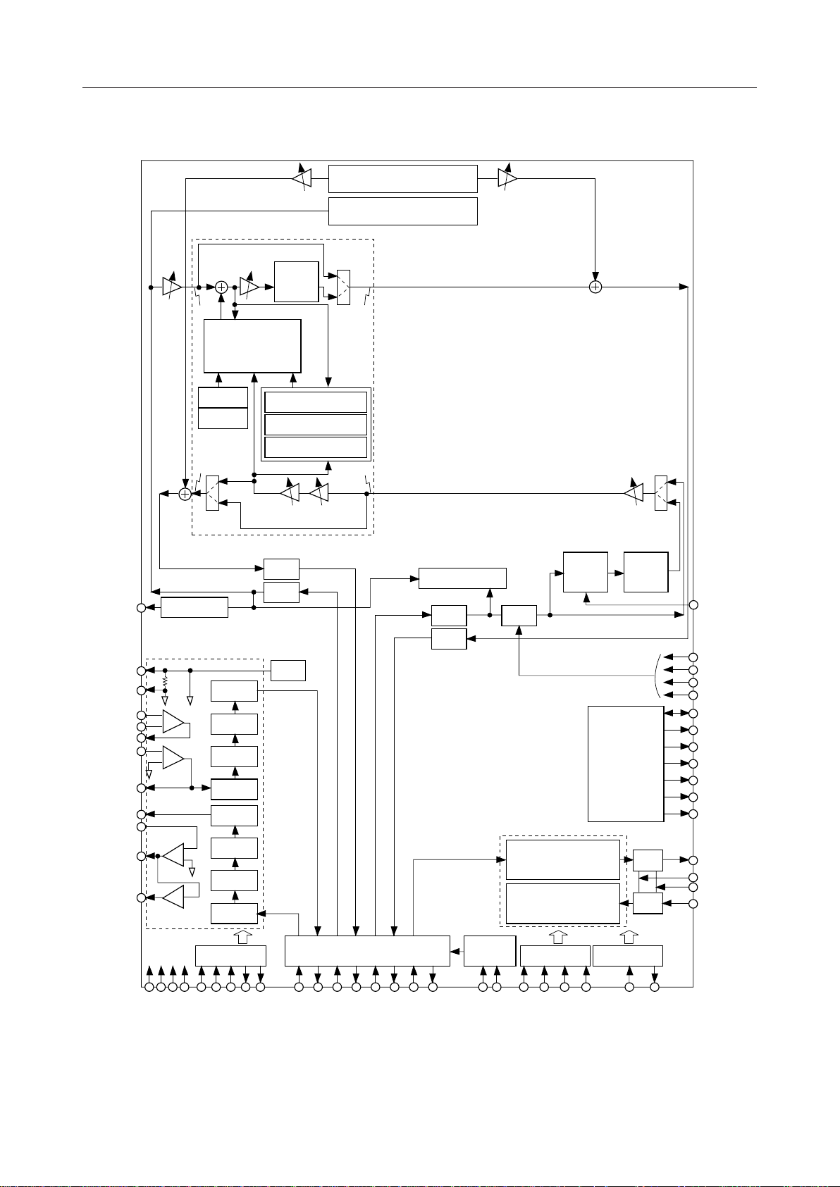
BLOCK DIAGRAM
MSM7718-01
VOXO
SGR
SGT
AIN1–
AIN1+
GSX1
AIN2
GSX2
VFRO
PWI
AOUT–
AOUT+
ATTtx
SinL
RoutL
Voice Detect
PCM CODEC
–
+
–
+
1.2 kW
–
+
–1
1.2 kW
ATTtgrx
ATTsL
+
–
Line
Adapive FIR Filter
(LAFF)
Coeff.L0
Coeff.L1
Howling Detector
Double Talk Detector
GainL ATTrL
Line Echo Canceler
L/m
m/L
VREF
L/m
BPF
ADC
RC LPF
RC LPF
DAC
LPF
m/L
Center
Clip
Power Calc.
Tone Generator (DTMF etc.)
Tone Detector (DTMF etc.)
SoutL
RinL
2100 Hz Detect
m/L
L/m
ATTtgtx
ATTrx
Power
Detect
Mute
Flash
Memory
Controller
(Reserved)
ADPCM TRANSCODER
ADPCM
CODER
ADPCM
DECODER
Noise
Gen.
P/S
S/P
VOXI
MLV0
MLV1
MLV2
MUTE
D7-0
A20-0
WE
OE
CS1
CS2
RP
IS
BCLKA
SYNCA
IR
DDA
V
DDD1,2,3
DG1,2,3
V
MCU Interface
AG
DEN
EXCK
DIN
INT
DOUT
PCMPCI
PCMPCO
P/S&S/P
PCMLNI
PCMLNO
PCMACI
PCMACO
PCMADI
PCMADO
Timing
Gen.
SYNCP
BCLKP
MCKSL
Clock Gen.
MCK
PDN/RST
Test Interface
PDWN
TSTO
TSTI1-4
2/38
Page 3
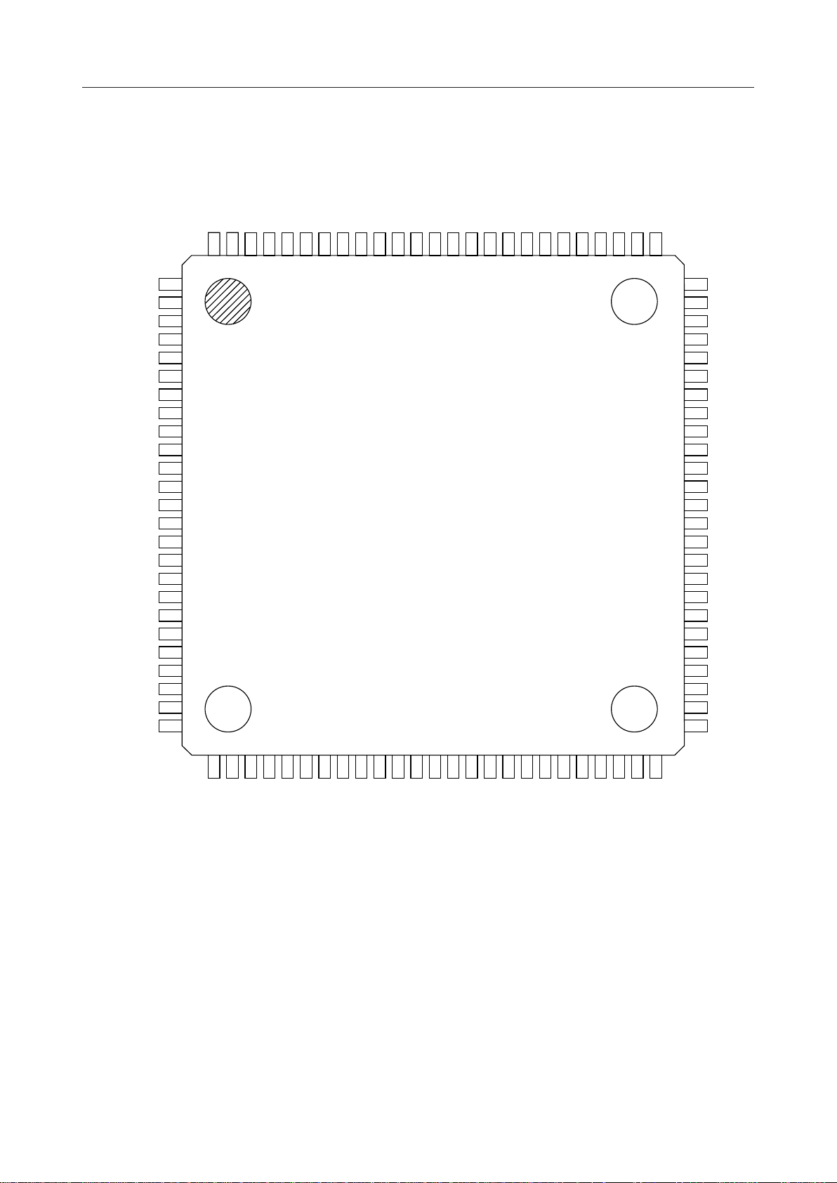
¡ Semiconductor
MSM7718-01
NC
DDD1
DDD3
V
TSTI1
BCLKA
SYNCA
IR
BCLKP
NC
PCMPCI
PCMLNI
PCMACI
PCMADI
DOUT
IS
PCMPCO
PCMLNO
DG3
PCMACO
PCMADO
NC
82
83
84
85
86
87
88
89
90
91
92
93
94
95
96
97
98
99
100
1
2TSTI2
3PDN/RST
4DIN
5EXCK
6DEN
7V
8SYNCP
9TSTI4
10TSTI3
11MCK
12MCKSL
13GNDA
14VFRO
15PWI
16AOUT–
17AOUT+
18SGT
19SGR
20NC
21NC
22AIN1–
23GSX1
24AIN1+
25NC
PDWN
81
RP
80
WE
79
OE
78
CS1
77
NC
76
75
74
73
72
71
70
69
68
67
66
65
64
63
62
61
60
59
58
57
56
55
54
53
52
51
NC
CS2
INT
TSTO
VOXO
VOXI
MLV0
MLV1
MLV2
MUTE
DG2
D7
NC
D6
D5
D4
D3
D2
D1
D0
A0
A1
A2
V
DDD2
NC
26
NC
27
GSX2
28
AIN2
29
V
DDA
30
DG1
37
36
35
34
33
32
31
NC
A15
A16
A17
A18
A19
A20
NC: No-connect pin
100-Pin Plastic TQFP
38
A14
39
A13
40
A12
41
A11
42
A10
43
A9
44
A8
45
A7
46
A6
47
A5
48
A4
49
A3
50
NC
3/38
Page 4
¡ Semiconductor
MSM7718-01
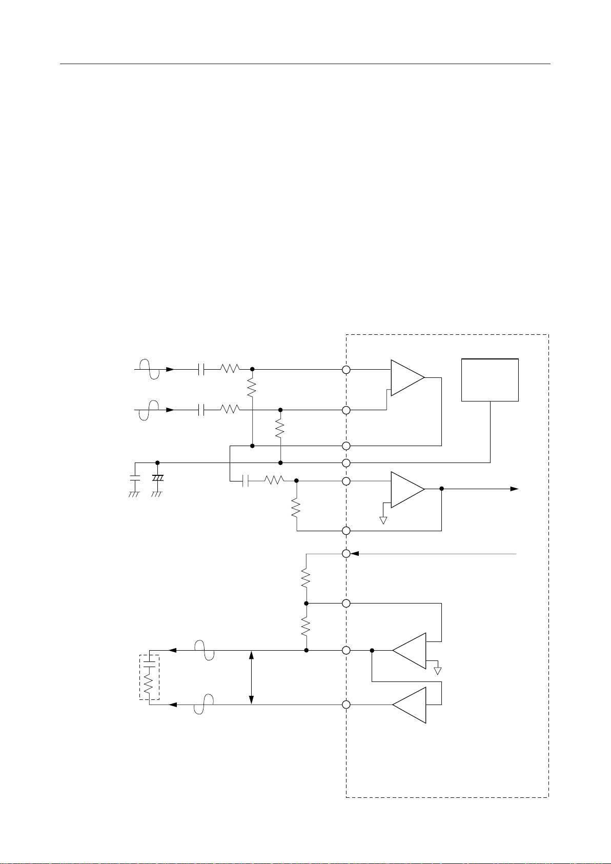
PIN FUNCTIONAL DESCRIPTION
AIN1+, AIN1–, AIN2, GSX1, GSX2
Transmit analog inputs and the outputs for transmit gain adjustment.
AIN1– (AIN2) connects to inverting input of the internal transmit amplifier. AIN1+ connects to noninverting input of the internal transmit amplifier. GSX1 (GSX2) connects to the internal transmit
amplifier output. Refer to Fig.1 for gain adjustment.
VFRO, AOUT+, AOUT–, PWI
Receive analog outputs and the output for receive gain adjustment.
VFRO is the receive filter output. AOUT+ and AOUT– are differential analog signal outputs which
can directly drive ZL (= 350 W + 120 nF) or a 1.2 kW load. Refer to Fig.1 for gain adjustment.
However, these outputs are in high impedance state during power-down.
Differential
Analog Input
V1
+
–
Transmit Gain: V
= (R2/R1) ¥ (R4/R3)
Receive Gain: V
= 2 ¥ (R5/R6)
C1
C1 R1
GSX2
O/VVFRO
R1
/Vi
C2
R2
R3
R2
R4
R6
R5
AIN1–
AIN1+
GSX1
SGT
AIN2
GSX2
VFRO
PWI
AOUT–
–
+
–
+
–
VREF
to ENCODER
from DECODER
ZL=120 nF + 350 W
Differential
V
O
Analog
Output
AOUT+
Figure 1 Analog Interface
+
–1
4/38
Page 5

¡ Semiconductor
MSM7718-01
SGT, SGR
Outputs of the analog signal ground voltage.
SGT outputs the analog signal ground voltage of the transmit system, and SGR outputs the analog
signal ground voltage for the receive system. The output voltage is approximately 1.4 V. Connect
bypass capacitors of 10 mF and 0.1 mF (ceramic type) between these pins and the AG pin. However
to reduce the response time of the receiver power-on, it is recommended to apply bypass capacitors
of 1 mF and 0.1 mF. During power-down, the output changes to 0 V.
AG
Analog ground.
DG1, 2, 3
Digital ground.
V
DDA
+3 V power supply for analog circuits.
V
DDD1, 2, 3
+3 V power supply for digital circuits.
PDN/RST
Power-down reset control input.
A logic “0” makes the LSI device enter a power-down state. At the same time, all control register
data is reset to the initial state. Set this pin to a logic “1” during normal operating mode. Since the PDN/
RST pin is ORed with CR0-B5 of the control register, set CR0-B5 to digital “0” when using this pin.
PDWN
Power-down control input.
When set to a logic “0”, the device changes to the power-down state, but each bit of control register
and internal variables of control register are retained. During normal operation, set this pin to logic
“1”. Since the PDWN pin is ORed with CR0-B6 of the control register, set CR0-B6 to logic “0” when
using this pin.
MCK
Master clock input.
The frequency must be 9.6 MHz or 19.2 MHz. The master clock signal is allowed to be asynchronous
with SYNCP, SYNCA, BCLKP, and BCLKA.
5/38
Page 6

¡ Semiconductor
MCKSL
Master clock selection input.
Set MCKSL to logic “0” when the master clock frequency is 9.6 MHz, and to logic “1” when it is 19.2
MHz.
PCMPCO
PCM data output of the PCM CODEC.
PCM is output from MSB, synchronizing with the rising edge of BCLKP and SYNCP. This pin is in
a high impedance state except during 8-bit PCM output. (It is also in a high impedance state during
power-down mode.) A pull-up resistor must be connected to this pin because its output is configured
as an open drain.
PCMPCI
PCM data input of the PCM CODEC.
PCM is shifted in at the falling edge of the BCLKP signal. The start of the PCM data (MSB) is
identified at the rising edge of SYNCP.
MSM7718-01
PCMADO
PCM data output of the ADPCM transcoder.
PCM is the output data after ADPCM decoder processing and is serially output from MSB in
synchronization with the rising edge of BCLKP and SYNCP. However, this signal timing can be
controlled at PCM multiplexing by the control register CR1-B5.
(The time slot 1 or 2 can be selected. Refer to Figs. 2-4.)
This pin is in a high impedance state except during 8-bit PCM output. (It is also in an high impedance
state during power-down mode.) A pull-up resistor must be connected to this pin because its output
is configured as an open drain.
PCMADI
PCM data input of the ADPCM transcoder.
PCM is shifted in at a falling edge of the BCLKP signal and input from MSB. The start of the PCM
data (MSB) is identified at the rising edge of SYNCP. However, this signal timing can be controlled at PC M
multiplexing by the control register CR1-B5.
(The time slot 1 or 2 can be selected. Refer to Figs. 2-4.)
PCMLNO
PCM receive data output of the line echo canceler.
PCM is output from MSB in a sequential order, synchronizing with the rising edge of BCLKP and
SYNCP. However, this signal timing can be controlled at PCM multiplexing by the control
register CR2-B3 to B5.
(The time slot of 1 to 7 can be selected. Refer to Figs. 2-4.)
This pin is in a high impedance state except during 8-bit PCM output. (It is also in a high impedance
state during power-down mode.) A pull-up resistor must be connected to this pin because its output
is configured as an open drain.
6/38
Page 7
¡ Semiconductor
MSM7718-01
PCMLNI
PCM transmit data input of the line echo canceler.
PCM is shifted in at a falling edge of the BCLKP signal and input from MSB. The start of the PCM
data
(MSB) is identified at the rising edge of SYNCP. However, this signal timing can be controlled
at PCM
mutiplexing by the control register CR2-B3 to B5.
(One of the time slots 1 to 7 can be selected. Refer to Figs. 2-4.)
PCMACO
PCM transmit data output of the line echo canceler.
PCM is output from MSB in a sequential order, synchronizing with the rising edge of BCLKP and
SYNCP. However, this signal timing can be controlled at PCM multiplexing by the control
register CR2-B0 to B2. (The time slot 1 to 7 can be selected. Refer to Figs. 2 - 4.)
This pin is in a high impedance state except during 8-bit PCM output.
(It is also in a high impedance sate during power down mode.) A pull-up resistor must be connected
to this pin because its output is configured as an open drain.
PCMACI
PCM receive data input of the line echo canceler.
PCM is shifted in at a falling edge of BCLKP and input from MSB.
The start of the PCM data (MSB) is identified at the rising edge of SYNCP. However, this signal
timing can be controlled at PCM multiplexing by the control register CR2-B0 to B2. (One of the time
slots 1 to 7 can be selected. Refer to Figs. 2-4.)
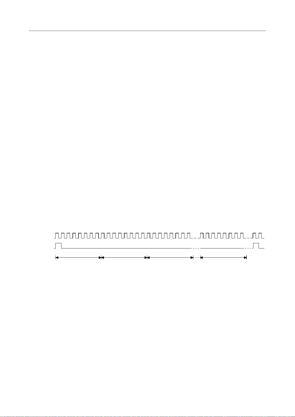
BCLKP
SYNCP
PCM
Multiple
time slot 1 time slot 2 time slot 3 time slot 7
Note : The PCM signals (PCMPCI and PCMPCO) of the PCM CODEC are always assigned to time
slot 1.
The PCM signals (PCMADI and PCMADO) of the ADPCM transcoder can be assigned to
time slot 1 or 2.
The PCM signals (PCMLNI, PCMLNO, PCMACI, PCMACO) of the line echo canceler can
be assigned to one of the time slots 1 to 7. (Multiple timing is controlled by CR1 and CR2.)
Figure 2 PCM Multiple Timing
7/38
Page 8
¡ Semiconductor
MSM7718
MSM7718-01
Line Echo
Canceler
Line Slave telephone
PCM
CODEC
PCMPCO
PCMPCI
PCMLNI
PCMLNO
PCMACI
PCMACO
PCMADI
ADPCM
Transcoder
PCMADO
Note : In this connection, PCMLNI, PCMLNO, PCMACI, and PCMACO should all be assigned
to time slot 1 for their output timing (the output timing for the PCM CODEC is always
assigned to time slot 1).
Turn on the line echo canceler and establish a route between the slave telephone and the
line.
Figure 3 PCM Signal Connection Example 1
8/38
Page 9
¡ Semiconductor
MSM7718
MSM7718-01
Line Echo
Canceler
Line Slave telephone
Microphone
and speaker
of the master
telephone
PCM
CODEC
PCM
CODEC
PCMPCO
PCMPCI
PCMLNI
PCMLNO
PCMACI
PCMACO
PCMADI
ADPCM
CODEC
PCMADO
Notes : The PCM signals of the ADPCM transcoder are assigned to time slot 2. (The PCM signals
of the PCM CODEC are always assigned to time slot 1.) The PCM signals of an external
PCM CODEC are assigned to time slot 3.
Route between the line and the slave telephone
PCMLNI and PCMLNO are assigned to time slot 1 and PCMACI and PCMACO are
assigned to time slot 2.
Turn on the line echo canceler, and establish the route between the line and the slave
telephone.
Route between the master telephone's microphone/speaker (handsfree) and the slave
telephone
PCMLNI and PCMLNO are assigned to time slot 3 and PCMACI and PCMACO are
assigned to time slot 2.
Turn on the line echo canceler, and establish the
speaker of the master telephone and the
slave telephone.
route between the microphone/
Route between the line and the master telephone's microphone/speaker (handsfree)
PCMLNI and PCMLNO are assigned to time slot 1 and PCMACI and PCMACO are
assigned to time slot 3.
Put the line echo canceler into “through mode”, and establish the route between
the line and the microphone/speaker of the master telephone.
Various routing can be implemented providing extension of external PCM CODECs.
Figure 4 PCM Signal Connection Example 2
9/38
Page 10

¡ Semiconductor
BCLKP
Shift clock input for the PCM data (PCMPCO, PCMPCI, PCMADO, PCMADI, PCMLNO, PCMLNI,
PCMACO, PCMACI). The frequency is set in the range of 64 kHz to 2048 kHz.
This signal must be synchronized with the SYNCP signal. (Refer to Fig. 2.)
SYNCP
8 kHz synchronous signal input for transmit and receive PCM data.
This signal must be synchronized with the BCLKP signal. (Refer to Fig. 2.)
IS
Transmit ADPCM data output.
This data is the output data after ADPCM encoding, and is serially output from MSB in synchronization with the rising edge of BCLKA and SYNCA. This pin is an open drain output which remains
in a high impedance state during power-down, and requires a pull-up resistor.
MSM7718-01
IR
Receive ADPCM data input.
ADPCM is shifted in on the rising edge of BCLKA in synchronization with SYNCA and input
orderly from MSB.
BCLKA
Shift clock input for the ADPCM data (IS, IR).
The frequency is from 64 kHz to 2048 kHz.
This signal must be synchronized with the SYNCA signal.
SYNCA
8 kHz synchronous signal input for transmit and receive ADPCM data.
Synchronize this data with BCLKA signal. SYNCA is used for indicating the MSB of the serial
ADPCM data stream.
DEN, EXCK, DIN, DOUT, INT
Serial control ports for MCU interface.
Reading and writing data is performed by an external MCU through these pins. 17-byte control
registers are provided in this device.
DEN is the “Enable” control signal input, EXCK is the data shift clock input, DIN is the address and
data input, and DOUT is the data output.
Input/output timing is shown in Fig. 5.
INT goes to logic “0” when any change has been found in the tone detection results in the tone
detection mode (change in the control register bits CR7-B3, B2), and goes to logic “1” when the data
of control register CR7 is read out.
10/38
Page 11
¡ Semiconductor
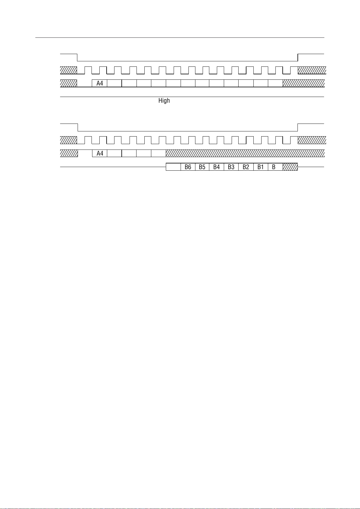
,
DEN
EXCK
MSM7718-01
DIN
DOUT
DEN
EXCK
DIN
DOUT
W
A4
A4
R A2A1A0
High Impedance
A3
A3
A2
A1 A0 B7 B6 B5 B4 B3 B2 B1 B0
High Impedance
(a) Data Write Timing
B6 B5 B4 B3 B2 B1 B0
B7
(b) Data Read Timing
Figure 5 MCU Interface Input/Output Timing
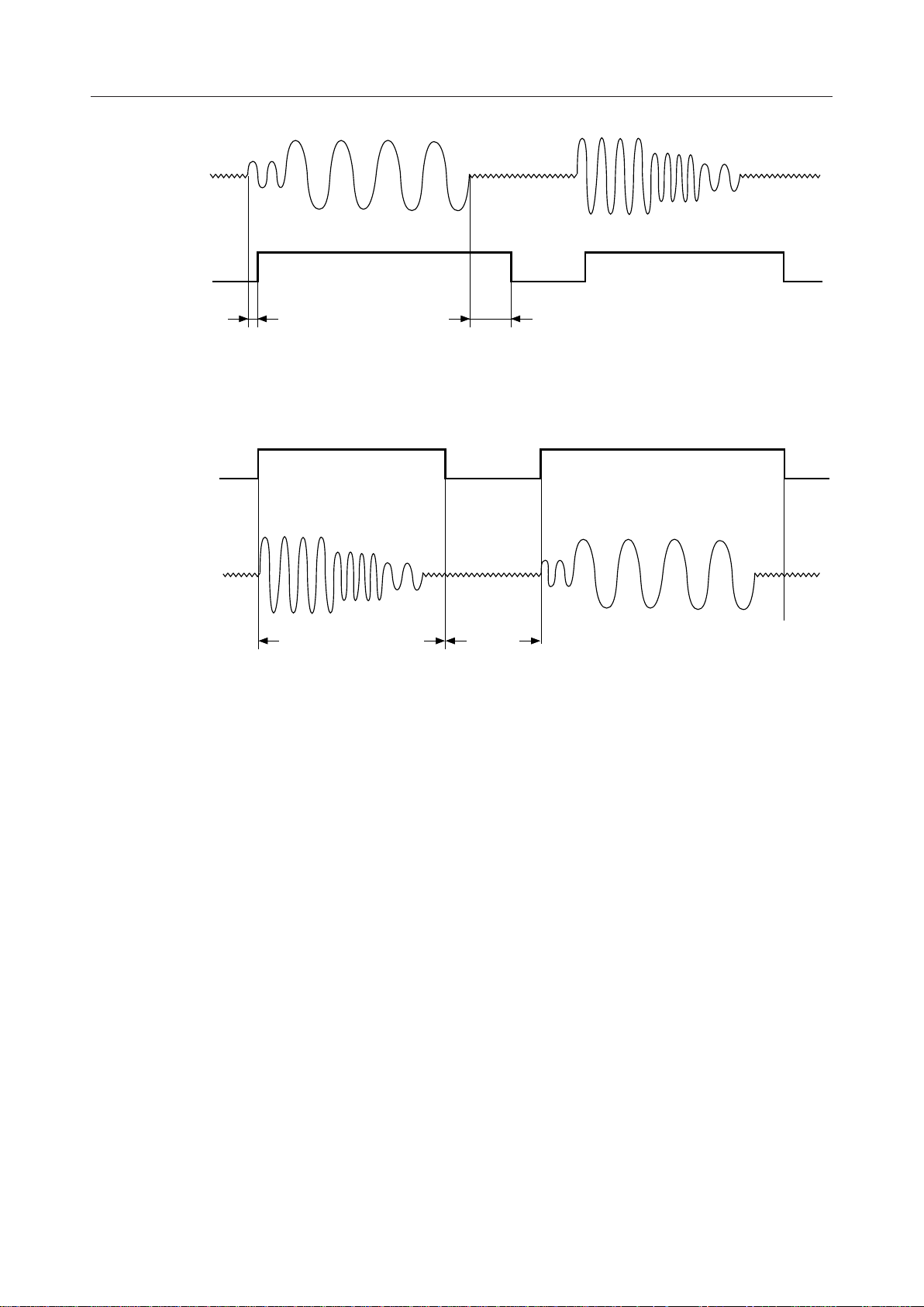
VOXO
Signal output for transmit VOX function.
The VOX function recognizes the presence or absence of the transmit voice signal by detecting the
level of the transmit signal to the line echo canceler . “1” and “0” levels set to this pin correspond
to the presence and the absence of voice, respectively. This result appears also at the register data
CR7-B7. The signal energy detect threshold is set by the control register data CR6-B6, B5.
The timiging diagram of the VOX function is shown in Fig 6.
The transmit signal to the line echo canceler refers to the signal input to the PCMLNI pin.
VOXI
Signal input for receive VOX function.
The “1” level at VOXI indicates the presence of a voice signal, the decoder block processes normal
receive signal, and the voice signal on the PCMACI pin goes through. The “0” level indicates the
absence of a voice signal and the background noise generated in this device is output to the line echo
canceler.
The background noise amplitude is set by the control register CR6.
Because this signal is ORed with the register data CR6-B3, set the control register data CR6-B3 to logic
“0”.
11/38
Page 12
¡ Semiconductor
g
Voice Input
GSX2
MSM7718-01
Silence
VOXO
T
VXON
Voice
Detect
Voice
T
VXOFF
Silence
Detect (Hangover time)
(a) Transmit VOX Function Timing Diagram (for Analog Input)
Silence
VOXI
Voice Output
VFRO
Normal Voice Signal
Decoded Time Period
(b) Receive VOX Function (CR6-B3: lo
Voice
Background
Noise
ic “0”) Timing Diagram (for Analog Input)
Voice
Voice
Note: The VOX function is valid when CR6-B7 is set to logic “1”.
Figure 6 VOX Function
MUTE
This pin is used to enable the receive side voice path mute level.
To set the mute level, set this pin to “1”.
MLV0, MLV1, MLV2
These pins are used to set the receive side voice path mute level.
For the control method, refer to the control register description (CR1). Since these pins are ORed
with CR1-B2, B1, and B0 internally, set the bits of the register to “0“ before using this pin.
12/38
Page 13

¡ Semiconductor
D7 to D0 (reserved for external memory I/F)
Output of write data, and input-output of read data.
A20 to A0 (reserved for external memory I/F)
External memory address output.
WE (reserved for external memory I/F)
Output for write control .
OE (reserved for external memory I/F)
Output for read control.
CS1, CS2 (reserved for external memory I/F)
MSM7718-01
Chip select output.
RP (reserved for external memory I/F)
Reset/power-down control output for external memory.
TSTI1, TSTI2, TSTI3, TSTI4
Input for test.
Normally fix these pins to logic “0”.
TSTI4
Input for mode select.
Fix this pin to logic “0” for normal speech mode.
Fix this pin to logic “1” for line echo canceler expansion mode. Refer to the explanation of CR0
for the operation mode.
TSTO
Output for test.
13/38
Page 14

¡ Semiconductor
ABSOLUTE MAXIMUM RATINGS
MSM7718-01
Parameter
Power Supply Voltage
Analog Input Voltage
Digital Input Voltage
Storage Temperature
Symbol
V
DD
V
AIN
V
DIN
T
STG
Condition
—
—
—
—
RECOMMENDED OPERATING CONDITIONS
Parameter
Power Supply Voltage
Operating Temperature
Input High Voltage
Input Low Voltage
Digital Input Rise Time
Digital Input Fall Time
Master Clock Frequency
Master Clock Duty Ratio
Bit Clock Frequency
Synchronous Pulse Frequency
Clock Duty Cycle
Transmit Sync Pulse Setting Time
Receive Sync Pulse Setting Time
Receive Sync Pulse Setting Time
PCM, ADPCM Setup Time
PCM, ADPCM Hold Time
Symbol
V
DD
Ta
V
IH
V
IL
t
Ir
t
If
f
MCK
D
C
f
BCK
f
SYNC
D
CK
t
XS
t
SX
t
XO
t
RS
t
SR
t
RO
t
WS
t
DS
t
DH
Condition
—
—
All digital inputs
All digital inputs
All digital inputs
All digital inputs
MCK
MCK
BCLKP, BCLKA
SYNCP, SYNCA
BCLKP, BCLKA, EXCK
BCLKP to SYNCP,
BCLKA to SYNCA
SYNCP to BCLKP,
SYNCA to BCLKA
SYNCP to BCLKP, SYNCA to BCLKA
BCLKP to SYNCP,
BCLKA to SYNCA
SYNCP to BCLKP,
SYNCA to BCLKA
SYNCP to BCLKP, SYNCA to BCLKA
SYNCP, SYNCA
—
—
Rating
–0.3 to +5
– 0.3 to V
–0.3 to V
–55 to +150
DD
DD
+ 0.3
+ 0.3
Unit
V
V
V
°C
(VDD = 2.7 V to 3.6 V, Ta = –25°C to +70°C)
Min.
2.7
–25
Typ.
—
+25
Max.
3.6
+70
Unit
V
°C
0.45
¥ V
DD
0
—
—
100ppm
–
40
64
1000ppm
–
40
100
100
100
100
1 BCLK
100
100
—
—
—
—
19.2/9.6
50
—
8.0
50
—
—
——
—
—
——
—
—
—
—
0.16
¥ V
DD
50
50
+100ppm
60
2048
+1000ppm
60
—
—
100
—
—
100
100
—
—
V
V
ns
ns
MHz
%
kHz
kHz
%
ns
ns
ns
ns
ns
ns
ms
ns
ns
Note: If SYNCP and SYNCA are generated from different clocks, do not change the relative
timing of the rising edge of SYNCP and that of SYNCA (that is, which rising edge is
earlier) after the reset state has been released.
14/38
Page 15

¡ Semiconductor
ELECTRICAL CHARACTERISTICS
DC Characteristics
Parameter Symbol Condition Min. Typ. Max. Unit
Power Supply Current 1
Power Supply Current 2
Input Leakage current
High Level Digital
Output Voltage
Low Level Digital
Output Voltage
Digital Output
Leakage Current
Input Capacitance
I
I
V
V
V
C
Operating mode, no signal
DD1
(only the master clock is input)
Power down mode
DD2
(only the master clock is input)
I
V
IH
I
IL
OH1
OH2
OL
I
O
IN
I=VDD
VI= 0 V
= 0.4 mA
I
OH
= 1 mA
I
OH
1LSTTL, pull-up resistance : 500 W
IS
—
MSM7718-01
(V
= 2.7 to 3.6 V, Ta= –25 to +70°C)
DD
—2240mA
— 0.2 1 mA
—— 2 mA
— — 0.5 mA
0.5¥V
0.8¥V
0 0.2 0.4 V
——10mA
—5—pF
—VDDV
DD
—VDDV
DD
Analog Interface Characteristics
Parameter Symbol Condition Min. Typ Max. Unit
Input Resistance
Output Load Resistance
Output Load Capacitance
Output Voltage Level (*1)
Offset Voltage
SGT, SGR Output Voltage
SGT Output Impedance
SGR Output Impedance
V
V
R
R
R
IN
R
L1
R
L2
R
L3
C
L1
C
L2
C
L3
V
O1
V
O2
V
O3
OFGX
OFGX
V
SG
SGT
SGR
(VDD= 2.7 to 3.6 V, Ta= –25 to +70°C)
AIN+, AIN–, AIN2, PWI
GSX1, GSX2, VFRO
AOUT+
AOUT–
GSX1, GSX2, VFRO
AOUT+
10——MW
20——kW
1.2 — — kW
1.2 — — kW
— — 100 pF
— — 100 pF
AOUT– — — 100
GSX1, GSX2, VFRO
=20kW)
(R
L
— — 1.3
AOUT+ (RL=1.2 kW) — — 1.3
AOUT– (RL=1.2 kW)
VFRO
VFRO
SGT, SGR
SGT
SGR
— — 1.3 V
–100 — +100
–20 — +20
— 1.4 —
—4080
—4 8
pF
V
PP
V
PP
PP
mV
mV
V
kW
kW
*1 –7.7 dBm (600 W) = 0 dBm0, +3.14 dBm0=1.30 V
PP
15/38
Page 16

¡ Semiconductor
Digital Interface Characteristics
Parameter Symbol Condition Min. Typ. Max. Unit
Digital Output Delay Time
PCM, ADPCM Interface
Serial Port
Digital Input/Output
Setting Time
Shift Clock Frequency
t
SDX
t
XD1
t
XD2
t
XD3
t
t
t
t
t
t
t
t
t
t
M10
t
M11
t
M12
f
ECK
, t
, t
, t
, t
M1
M2
M3
M4
M5
M6
M7
M8
M9
SDR
RD1
RD2
RD3
1LSTTL+100 pF
pull-up resistance : 500 W
Values in parentheses apply when
Cload = 10 pF,
pull-up resistance :£2 kW
Cload=100 pF
EXCK
MSM7718-01
(V
= 2.7 to 3.6 V, Ta= –25 to +70°C)
DD
0 — 200 (100) ns
0 — 200 (100) ns
0 — 200 (100) ns
0 — 200 (100) ns
50 — — ns
20 — — ns
20 — —
50 —
100 —
50 — —
50 — —
0——
50 — —
50
——
0
100
——
—— 10
—
—
ns
ns
ns
ns
ns
ns
ns
ns
ns——
ns
MHz
PCM/ADPCM Output Timing
BCLKP
SYNCP
PCMPCO
PCMADO
PCMLNO
PCMACO
t
0
XS
t
SDX
t
12345678910
t
XO
t
SX
XD1
t
t
WS
XD2
t
XD3
MSB LSB
Note : The timing for PCMADO, PCMLNO, and PCMACO shown above reperesents the timing
when time slot 1 is selected.
BCLKA
SYNCA
IS
t
XS
t
SDX
t
XO
123456789100
t
SX
t
XD1
t
XD2
MSB LSB
t
XD3
16/38
Page 17

¡ Semiconductor
PCM/ADPCM Input Timing
MSM7718-01
BCLKA
SYNCA
IR
BCLKP
SYNCP
PCMPCI
PCMADI
0 10
t
RS
0 10
t
RS
123456789
t
SR
t
RO
MSB
t
WS
t
t
DH
DS
LSB
123456789
t
SR
t
RO
MSB
t
t
DH
DS
LSB
PCMLNI
PCMACI
Note : The timing for PCMADI, PCMLNI, and PCMACI shown above represents the timing when
time slot 1 is selected.
Serial Port Timing for Microcontroller Interface
DEN
EXCK
DIN
DOUT
t
t
M2
123567
t
t
M1
M3
t
M4
t
M6
W/R A4 A1 A0
t
M5
13 14
t
M7
B7
t
M8
B7
B1 B0
B1 B0
15
t
M9
t
M10
M12
t
M11
17/38
Page 18

¡ Semiconductor
AC Characteristics
Parameter
Transmit Frequency Response
Receive Frequency Response
Transmit Signal to Distortion
Receive Signal to Distortion
Transmit Gain Tracking
Receive Gain Tracking
Idle Channel Noise
Absolute Signal Amplitude
Power Supply Noise
Rejection Ratio
Symbol
T1
L
OSS
L
T2
OSS
L
T3
OSS
L
T4
OSS
L
T5
OSS
L
T6
OSS
L
R1
OSS
L
R2
OSS
L
R3
OSS
L
R4
OSS
L
R5
OSS
SD T1
SD T2
SD T3
SD T4
SD T5
SD R1
SD R2
SD R3
SD R4
SD R5
GT T1
GT T2
GT T3
GT T4
GT T5
GT R1
GT R2
GT R3
GT R4
GT R5
N
IDLT
N
IDLR
A
VT
A
VR
P
SRRT
P
SRRR
(V
DD
Condition
Freq.(Hz) level (dBm0) Others
0-60
300-3k
1020
3300
0—
0—
3400
3968.75
0-3000
1020
3300
0 —
3400
3968.75
3
0
1020
–30 (*2)
–40
–45
3
0
1020
–30
(*2)
–40
–45
3
–10
1020
–40
—
–50
–55
3
–10
1020
–40
——
–50
–55
—
—
1020
Noise Freq.:
0 to 50 kHz
AIN=SG
(*3)
0
Noise Level:
50 mVpp
(*2)
(*2)
GSX2
VFRO
—
MSM7718-01
= 2.7 to 3.6 V, Ta = –25 to +70°C)
Min. Typ. Max. Unit
25——
–0.15 — +0.2
–0.15 — +0.8
0 — 0.8
13——
–0.15 — +0.2
–0.15 — +0.8
0 — 0.8
13——
35——
35——
35——
28——
23——
35——
35——
35——
28——
23——
–0.2 — +0.2
–0.2 — +0.2
–0.5 — +0.5
–1.2 — +1.2
–0.2 — +0.2
–0.2 — +0.2
–0.5 — +0.5
–1.2 — +1.2
——
——
0.285 0.32(*4) 0.359
0.285 0.32(*4) 0.359
30——
30——
—
Reference
Reference
Reference
Reference
–68
(–75.7)
–72
(79.7)
dB
dB
dB
dB
dB
dB
dBm0p
(dBmp)
dBm0p
(dBmp)
Vrms
Vrms
dB
dB
*2. P-message weighted filter used
*3. PCMPCI input code: “11111111” (m-law)
*4. 0.320 Vrms=0 dBm0=–7.7 dBm
Note : All ADPCM coder and decoder characteristics fully comply with ITU-T Recommendations
G.726.
18/38
Page 19

¡ Semiconductor
MSM7718-01
AC Characteristics (DTMF and Other Tones)
(V
= 2.7 to 3.6 V, Ta = –25 to +70°C)
DD
Parameter Symbol Condition Min. Typ. Max. Unit
Frequence Deviation
Tone Reference
Output Level
(*5)
Df
Df
T1
T2
V
TL
V
TH
V
RL
V
RH
Transmit side tone
(Gain set value:0dB)
Recieve side tone
(Gain set value:0dB)
DTMF Tones
Other various tones
DTMF (Low group)
DTMF (High group), Others
DTMF (Low group)
DTMF (High group), Others
–1.5 — +1.5 %
–1.5 — +1.5 %
–10 –8 –6 dBm0
–8 –6 –4 dBm0
–10 –8 –6 dBm0
–8 –6 –4 dBm0
Relative Value of
DTMF Tones
R
DTMF
V
TH/VTL, VRH/VRL
123dB
*5 Not including programmable gain set values
AC Characteristics (Gain Settings)
= 2.7 to 3.6 V, Ta = –25 to +70°C)
(V
DD
Parameter Symbol Condition Min. Typ. Max. Unit
Transmit/Recieve Gain
Setting Accurancy
D
G
For all gain set values –1 0 +1 dB
AC Characteristics (VOX Function)
Parameter Symbol Condition Min. Typ. Max. Unit
t
VXON
voice signal ON/OFF Detect Time
Transmit VOX Detection Level
Accuracy (Voice Detection Level)
t
VXOFF
D
VX
SilenceÆvoice — 5 — msTransmit VOX Detection Time
VoiceÆsilence
VOXO pin:see Fig.6
Voice/silence
differential:10 dB
For detection level set values by
CRM6-B6,B5
(V
= 2.7 to 3.6 V, Ta = –25 to +70°C)
DD
140/300 160/320 180/340 ms
–2.5 0 +2.5 dB
19/38
Page 20

¡ Semiconductor
AC Characteristics (Tone Detect Function)
Parameter
CPT Detection Frequency
CPT Non-detection Frequency
CPT Detection Level
CPT Non-detection Level
CPT Input Signal Continuation Time
CPT Detection Delay Time
CPT Detection Hold Time
DTMF Detection Frequency
DTMF Non-detection Frequency
DTMF Detection Level
DTMF Non-detection Level
DTMF Input Signal continuation Time
DTMF Detection Delay Time
DTMF Detection Hold Time
ANS Detection Frequency
ANS Non-detection Frequency
ANS Detection Level
ANS Non-detection Level
ANS Input Signal Continuation Time
ANS Detection Delay Time
ANS Detection Hold Time
Symbol
f
detcp
f
rejcp
V
detcp
V
rejcp
t
detcp
t
rejcp
t
dlycp
t
holcp
f
detdt
f
rejdt
V
detdt
V
rejdt
t
detdt
t
rejdt
t
dlydt
t
holdt
f
detan
f
rejan
V
detan
V
rejan
t
detan
t
rejan
t
dlyan
t
holan
Input Frequency: 350 to 640 Hz –39 — 0 dBm0
CPT detected
CPT not detected
At Nominal Frequency
At Nominal Frequency
Input Frequency:Nominal Frequency ±1.5%
CPT detected
CPT not detected
Input Frequency: 2079 to 2121 Hz
CPT detected
CPT not detected
MSM7718-01
= 2.7 to 3.6 V, Ta = –25 to +70°C)
(V
DD
Condition Min.
— 350 — 640 Hz
—
—
—
—
—
—
—
—
—
—
—
—
Typ. Max. Unit
700 — — Hz
— — 250 Hz
— — –49 dBm0
55 — — ms
— — 30 ms
30 45 55 ms
71624ms
— — ±1.5 %
±3.8 — — %
–39 — 0 dBm0
— — –47 dBm0
38 — — ms
— — 16 ms
16 — 38 ms
14 — 25 ms
2079 2100 2121 Hz
2350 — — Hz
— — 1900 Hz
–31 — 0 dBm0
— — –35 dBm0
480 — — ms
— — 420 ms
420 450 480 ms
71217ms
t
detXX
t
rejXX
INPUT SIGNAL
DETECPT: CR7-B3
DETDTMF: CR7-B2
DET21L: CR7-B1
DET21L: CR7-B1
t
dlyXX
t
holXX
INT pin
INT: CR7-B4 (positive logic)
The state of the INT pin is changed by reading the
contents of CR7. It is retained when CR7 is not read.
Note : In the case of call progress tone, DTMF tone, and 2100 Hz tone, XX refers to cp, dt, and
an respectively.
20/38
Page 21

¡ Semiconductor
y
FUNCTIONAL DESCRIPTION
Control Registers
Table 1 Control Register Map
MSM7718-01
Reg
Name
CR0 0 0
CR1 0 001
CR2 0 100
CR3 0 101
CR4 0 010
CR5 0 011
CR6 0 110
CR7 0 111
CR8 1 000
CR9 1 001
CR10 1 100
CR11 1 101
CR12 1 010
CR13 1 011
Address
A4
A3 A1
0
0
0
0
0
0
0
0
0
0
0
0
0
0
A2
A0
0
B7
0
— PDWN
ADPCM
MODE
PCM PCO
MUTE
TX
GAIN3TXGAIN2
TX TONE
GAIN3
DTMF/OTHERS
SEL
VOX
ON/OFFONLVL1
VOX
OUT
LECTHR
(HCL)*
AECTHR
(HCL)*
SEND/
REC
ST7/
A7
ST15/
A15
——
Contents
B6 B5 B4 B3 B2 B1 B0
ADPCM
RESET
PCM PCI
MUTE
TX TONE
GAIN2
TX TONE
SEND
Silence level
LECCLR1
MEM
ST6/
ST14/
Silence level
1
—
SEL
A6
A14
PDN/
RST
PCM AD
SELTXMUTERXMUTERXMLV2RXMLV1RXMLV0
PCM LN
SEL2
TX
GAIN1TXGAIN0RXGAIN3RXGAIN2RXGAIN1RXGAIN0
TX TONE
GAIN1
RX TONE
SEND
ON
LVL0
0
LECCLR2 LECHD
AECCLR
ADPCM
MODE1
ST5/
A5
ST13/
A13
—
—
PCM LN
SEL1
TX TONE
GAIN0
TONE4
OFF
TIME
INT
AECHD
ADPCM
MODE0
ST4/
A4
ST12/
A12
ST20/
A20
OPE
MODE3
PCM LN
SEL0
RX TONE
GAIN3
TONE3 TONE2 TONE1 TONE0
VOX
IN
DET
CPT
LECCCLP
(NLP)*
AECCCLP
(NLP)*
CMD3 CMD2 CMD1 CMD0
ST3/
A3
ST11/
A11
ST19/
A19
OPE
MODE2
PCM AC
SEL2
RX TONE
GAIN2
RX. NOISE
LEVEL SEL
DET
DTMF
LECHLD
(ADP)*
AECHLD
(APD)*
ST2/
A2
ST10/
A10
ST18/
A18
OPE
MODE1
PCM AC
SEL1
RX TONE
GAIN1
RX. NOISE
LVL1
BUSY/
DET21L
LECATT
(ATT)*
AECATT
(ATT)*
ST1/
A1
ST9/
A9
ST17/
A17
OPE
MODE0
PCM AC
SEL0
RX TONE
GAIN0
RX. NOISE
LVL0
RPM/
DET21A
LECGC
(GC)*
AECGC
(GC)*
ST0/
A0
ST8/
A8
ST16/
A16
R/W
R/W
R/W
R/W
R/W
R/W
R/W
R/W
R
R/W
R/W
R/W
R/W
R/W
R/W
CR14 1 110
CR15 1 111
CR16 0 000
CR17 0 001
CR18 0 100
R/W : Read/write enable R : Read only register
*
0
0
1
1
1
: These are the s
mbols of control pins used in the MSM7602 (echo canceler LSI device).
SP4SP5SP6SP7
SP12SP13SP14SP15
SP20———
D4/CA4D5/CA5D6/CA6D7/CA7
WA4WA5WA6WA7
SP3 SP2 SP1 SP0
SP11 SP10 SP9 SP8
SP19 SP18 SP17 SP16
D3/CA3 D2/CA2 D1/CA1 D0/CA0
D TONE3/
WA3
D TONE2/
WA2
D TONE1/
WA1
D TONE0/
WA0
R/W
R/W
R/W
R/W
R/W
21/38
Page 22

¡ Semiconductor
MSM7718-01
(1)CR0 (Basic operating mode settings)
B7 B6 B5 B4 B3 B2 B1 B0
CR0
Initial value *
— PDWN PDN/RST —
OPE
MODE3
00000000
OPE
MODE2
OPE
MODE1
OPE
MODE0
* : Indicates the value to be set when a resetting is made through the PDN/RST pin. (Also
when reset by bit 5 (B5, PDN/RST), the other bits of CR0 are reset to initial values.)
B7... Not used
B6... Power-down (entire system) 0: Power-on 1: Power-down
ORed with the inverted external power-down signals
Set the PDWN pin to “1” when this data is used. The control registers and their internal
variables are not reset.
B5... Power-down reset (entire system) 0: Power-on 1: Power-down reset
ORed with the inverted external power-down reset signals
Set the PDN/RST pin to “1” when this data is used .
B4... Not used
B3, 2, 1, 0 ...... Selection of an operating mode
(0, 0, 0, 0) : Initial mode
This mode enables a change (see Figure 15-1, 2) in memory that contains internal default values such
as tone generation frequencies.
In this mode, the PCM output pin acts to output idle patterns and the PCM input pin acts to
input idle patterns. When a reset or power-down occurs or when power down is released,
the device enters the initial mode about 200 ms after that.
(0, 0, 0, 1) : Reserved
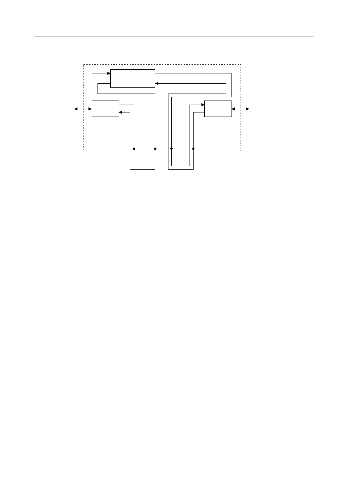
(0, 0, 1, 0) : Normal speech mode (see Figure 7-1)
This mode enables call services between a slave telephone and a line (including tone
generation) and detection of a DTMF tone and a call progress tone.
The internal process enables the tone detector. The ADPCM encoder/decoder, the tone
generator, and the line echo canceler become operative and can be controlled by the contents
of the control registers.
(0, 0, 1, 1) to (0, 1, 0, 0) : Reserved
(0, 1, 0, 1) : Line echo canceler expansion mode (see Figure 7-2)
This mode can expand the delay time of the line echo canceler up to 54 ms.
Concerning the internal processing, the ADPCM encoder/decoder, the line echo canceler, and
the tone generator become operative and can be controlled by the contents of the control
registers.
In addition, 2100 Hz tone of PCMLNI and PCMACI (bidirectional) can be detected.
(0, 1, 1, 0) to (1, 1, 1, 1) : Reserved
22/38
Page 23

¡ Semiconductor
Tone Generator
Tone Detector
23 ms Line
Echo Canceler
MSM7718-01
Note :
• When the MSM7718 is used in normal speech
mode, set the TSTI4 pin to “0”.
• In normal speech mode, the tone detector can
detect call progress tone and DTMF tone by
PMLNI input.
PCM CODEC
MSM7718
ADPCM CODER
ADPCM DECODER
Figure 7-1 Normal Speech Mode
Tone Generator
Tone Detector
54 ms Line
Echo Canceler
PCM CODEC
MSM7718
ADPCM CODER
ADPCM DECODER
Figure 7-2 Line Echo Canceler Expansion
Mode
Note :
• When the MSM7718 is used in line echo
canceler expansion mode, set the TSTI4 pin to
digital “1”.
• In line echo canceler expansion mode, the
tone detector can detect not only call progress
tone and DTMF tone by PMLNI input but
also 2100 Hz tone by PCMLNI and PCMACI
input (bidirectional).
• The PCM CODEC does not operate in this
mode. A capacitor is required between SGT
and ground and between SGR and ground
(see Application Circuit).
23/38
Page 24

¡ Semiconductor
MSM7718-01
(2) CR1 (Setting of ADPCM operating mode and PCM I/O signals)
B7 B6 B5 B4 B3 B2 B1 B0
CR1
Initial value
ADPCM
MODE
00000000
ADPCM
RESET
PCM AD
SEL
TX
MUTE
RX
MUTE
RX
MLV2
RX
MLV1
RX
MLV0
B7... ADPCM algorithm 0: 32 kbps (G.726) 1: Reserved
B6... Transmitter/receiver ADPCM resetting (conforming to G.726) 1: Reset
B5 ... PCM I/O multiple timing control (PCMADI and PCMADO pins) of the ADPCM CODEC
0: Time slot 1 1: Time slot 2
B4... Muting of transmitter ADPCM data 1: Mute
B3 ... Muting of receiver ADPCM data 1: Muting specified by bits B2, B1, and B0 is enabled.
This bit is valid when the MUTE pin is “0”.
B2, B1, B0... Setting of a receiver voice path mute level
(MLV2, MLV1, MLV0) = (0, 0, 0) : Through
(0, 0, 1) : – 6 dB
(0, 1, 0) : –12 dB
(0, 1, 1) : –18 dB
(1, 0, 0) : –24 dB
(1, 0, 1) : –30 dB
(1, 1, 0) : –36 dB
(1, 1, 1) : MUTE
24/38
Page 25

¡ Semiconductor
MSM7718-01
(3)CR2 (Setting of PCM I/O multiple control)
B7 B6 B5 B4 B3 B2 B1 B0
CR2
Initial value
PCM PCO
MUTE
00000000
PCM PCI
MUTE
PCM LN
SEL2
PCM LN
SEL1
PCM LN
SEL0
PCM AC
SEL2
PCM AC
SEL1
PCM AC
SEL0
B7... ON or OFF of the PCM signal of the transmitter side of the PCM CODEC (PCMPCO pin)
0: ON 1: OFF
When this bit is “1” (OFF), the PCMPCO pin transmits a PCM idle pattern.
B6... ON or OFF of the PCM signal of the receiver side of the PCM CODEC (PCMPCI pin)
0: ON 1: OFF
When this bit is “1” (OFF), the PCMPCI pin receives a PCM idle pattern.
B5, 4, 3.... PCM I/O multiple timing control (PCMLNI and PCMLNO pins) of the line echo canceler
(see Table 2)
B2, 1, 0.... PCM I/O multiple timing control (PCMACI and PCMACO pins) of the line echo canceler
(see Table 2)
Table 2 PCM Multiple Timing Control Table
B5 B4 B3
B2 B1 B0()
0 0 0 None
001 1
010 2
011 3
100 4
101 5
110 6
111 7
Corresponding time slot
Note : When bits B5 to B3 or B2 to B0 are all zeros, the internal process inputs a PCM idle pattern.
In this case, the outputs are all in high impedance state for all time slots.
25/38
Page 26

¡ Semiconductor
(4)CR3 (Transmit/receive gain adjustment)
B7 B6 B5 B4 B3 B2 B1 B0
CR3
Initial value
TX
GAIN3
00000000
TX
GAIN2
TX
GAIN1
TX
GAIN0
RX
GAIN3
B7, 6, 5, 4 ...... Adjustment of the transmit signal gain [ATTtx]
(see Table 3)
B3, 2, 1, 0 ...... Adjustment of the receive signal gain [ATTrx]
(see Table 3)
Table 3 Transmit/Receive Signal Gain Setting
RX
GAIN2
MSM7718-01
RX
GAIN1
GAIN0
RX
B7
1
1
1
1
1
1
1
1
B6 B5 B4
000
001
010
011
100
101
110
111
000 0 dB 0000 0 0 dB
001 +2 dB 0010 0 +2 dB
010 +4 dB 0100 0 +4 dB
011 +6 dB 0110 0 +6 dB
100 +8 dB 1000 0 +8 dB
1 0 1 +10 dB 1 0 10 0 +10 dB
1 1 0 +12 dB 1 1 00 0 +12 dB
1 1 1 +14 dB 1 1 10 0 +14 dB
Transmit signal gain
–16 dB
–14 dB
–12 dB
–10 dB
–8 dB
–6 dB
–4 dB
–2 dB
B3
1
1
1
1
1
1
1
1
This table is for gains of transmit/receive voice signals.
B2 B1 B0
000
001
010
011
100
101
110
111
Receive signal gain
–16 dB
–14 dB
–12 dB
–10 dB
–8 dB
–6 dB
–4 dB
–2 dB
26/38
Page 27

¡ Semiconductor
MSM7718-01
(5)CR4 (Adjustment of tone generator gain)
B7 B6 B5 B4 B3 B2 B1 B0
CR4
Initial value
TX TONE
GAIN3
00000000
TX TONE
GAIN2
TX TONE
GAIN1
TX TONE
GAIN0
RX TONE
GAIN3
RX TONE
GAIN2
RX TONE
GAIN1
RX TONE
GAIN0
B7, 6, 5, 4 ...... Transmit side gain adjustment for the tone generator [ATTtgtx] (see Table 4)
B3, 2, 1, 0 ...... Receive side gain adjustment for the tone generator [ATTtgrx] (see Table 5)
Table 4 Setting of Transmit Side Gain of Tone Generator
B7 B6 B5 B4
0000
0001
0010
0011
0100
0101
0110
0111
Table 5 Setting of Receive Side Gain of Tone Generator
B3 B2 B1 B0
0000
0001
0010
0011
0100
0101
0110
0111
Tone generator gain
–36 dB
–34 dB
–32 dB
–30 dB
–28 dB
–26 dB
–24 dB
–22 dB
Tone generator gain
–36 dB
–34 dB
–32 dB
–30 dB
–28 dB
–26 dB
–24 dB
–22 dB
B7 B6 B5 B4
1000
1001
1010
1011
1100
1101
1110
1111
B3 B2 B1 B0
1000
1001
1010
1011
1100
1101
1110
1111
Tone generator gain
–20 dB
–18 dB
–16 dB
–14 dB
–12 dB
–10 dB
–8 dB
–6 dB
Tone generator gain
–20 dB
–18 dB
–16 dB
–14 dB
–12 dB
–10 dB
–8 dB
–6 dB
Settings of Table 5 are made in relation to the following tone levels:
DTMF tone (Low frequency group) : –2 dBm0
DTMF tone (High frequency group) and other tone : 0 dBm0
For example, when bits B3, B2, B1, and B0 are set to “1, 1, 1, 1” (–6 dB), the PCMLNO pin outputs a
tone of the following levels:
DTMF tone (Low frequency group) : –8 dBm0
DTMF tone (High frequency group) and other tone : –6 dBm0
The default value change command enables the gain adjustment by –1 dB step.
Writing “13CAh” into the address 00D8h adds a gain of –1 dB to the values in the above table. The
default value is “1634h”.
27/38
Page 28

¡ Semiconductor
(6)CR5 (Setting of tone generator operating mode and tone frequency)
B7 B6 B5 B4 B3 B2 B1 B0
CR5
Initial value
DTMF/OTHERS
SEL
00000000
TX TONE
SEND
RX TONE
SEND
TONE4
TONE3 TONE2 TONE1 TONE0
B7... Selection of DTMF signal or others (S, F, or R tone)
0: Others 1: DTMF signal
B6... Transmission of transmit side tone 0: Not transmit 1: Transmit
B5... Transmission of receive side tone 0: Not transmit 1: Transmit
B4, 3, 2, 1, 0 ... Setting of a tone frequency (see Table 6)
Table 6 Setting of Tone Generator Frequencies
(a) when B7 = “1” (DTMF tone)
MSM7718-01
B4 B3 B1 B0
*0 00
*0 01
*0 10
*0 11
*0 00
*0 01
*0 10
*0 11
B2
0
0
0
0
1
1
1
1
Description
697 Hz + 1209 Hz (1)
697 Hz + 1336 Hz (2)
697 Hz + 1477 Hz (3)
697 Hz + 1633 Hz (A)
770 Hz + 1209 Hz (4)
770 Hz + 1336 Hz (5)
770 Hz + 1477 Hz (6)
770 Hz + 1633 Hz (B)
B4 B3 B1 B0
*1 00
*1 01
*1 10
*1 11
*1 00
*1 01
*1 10
*1 11
B2
0
0
0
0
1
1
1
1
Description
852 Hz + 1209 Hz (7)
852 Hz + 1336 Hz (8)
852 Hz + 1477 Hz (9)
852 Hz + 1633 Hz (C)
941 Hz + 1209 Hz (*)
941 Hz + 1336 Hz (0)
941 Hz + 1477 Hz (#)
941 Hz + 1633 Hz (D)
(b) When B7 = “0” (Others)
The Table below lists default frequencies. “00000” to “00011” (“B4, B3, B2, B1, B0”) are tones,
which are modulated by sinewave. “01000” to “01011” are wamble tones, and “10000” to “10111”
are single tones. For procedures to change frequencies, see the next page.
B4 B3 B2 B1 B0
000 00
000 00
000 10
000 11
001 00
001 01
001 10
001 11
010 00
010 01
010 10
010 11
011 00
011 01
011 10
011 11
Description
400/0H – 16 Hz Sine wave modulation
3000/0H – 16 Hz Sine wave modulation
2700/0H – 16 Hz Sine wave modulation
*/*H – 16 Hz Sine wave modulation
—
—
—
—
513/636 Hz 12 Hz Wamble
800/1000 Hz 8 Hz Wamble
2000/2667 Hz 8 Hz Wamble
*/*Hz *Hz Wamble
—
—
—
—
B4 B3 B2 B1 B0
100 00
100 01
100 01
100 11
101 00
101 01
101 10
101 11
110 00
110 01
110 10
110 11
111 00
111 01
111 10
111 11
Description
400 Hz Single tone
1000 Hz Single tone
2000 Hz Single tone
2667 Hz Single tone
1300 Hz Single tone
2080 Hz Single tone
*Hz Single tone
*Hz Single tone
—
—
—
—
—
—
—
—
28/38
Page 29

¡ Semiconductor
MSM7718-01
Frequencies of tones (other than DTMF signals) to be generated by the tone generator can be changed.
Tone frequencies can be changed in the Initial mode. See Figure 15-1 for procedures to change tone
frequencies. The related subaddresses are shown below.
Modulation by 16 Hz sine wave
Modulation by 16 Hz sine wave
B4 B3 B2 B1 B0
Subaddress 1
(Frequency 1)
*1
00000
00001
00010
00011
Wamble
B4 B3 B2 B1 B0
01000
01001
01010
01011
Single tone
B4 B3 B2 B1 B0
164h
165h
166h
167h
Subaddress 1
(Frequency 1)
*1
168h 16Ch 170h 174h
169h 16Dh 171h 175h
16Ah 16Eh 172h 176h
16Bh 16Fh 173h 177h
Subaddress 1
(Frequency 1)
*1
62.5 ms
Subaddress 2
(Frequency 2)
*1
8 Hz wamble tone
Subaddress 3
(Time 1)
*2
Subaddress 4
(Time 2)
*2
10000
10001
10010
10011
10100
10101
10110
10111
178h
179h
17Ah
17Bh
17Ch
17Dh
17Eh
17Fh
Time 1
62.5 ms
Transmit single tone
Time 2
62.5 ms
*1 Transmitted Tone Frequency = A ¥ 8.192 (A = frequency)
ex. When frequency = 1000 Hz, 1000 ¥ 8.192 = 9011.2 = 9011d (eliminate after the decimal
point) = 2333h
*2 Wamble Frequency (Tone Transmit time) = (A/B)/2 – 1
(A = Transmitted tone frequency, B = wamble frequency)
ex. When wamble frequency is 8 Hz, tone frequency = 2667 Hz.
(2667/8)/2 – 1 = 166.69 = 166d (eliminate after the decimal point) = A6h
29/38
Page 30

¡ Semiconductor
MSM7718-01
(7)CR6 (VOX function control)
B7 B6 B5 B4 B3 B2 B1 B0
CR6
Initial value
VOX
ON/OFF
00000000
ON
LVL1
ON
LVL0
OFF
TIME
VOX
IN
RX. NOISE
LEVEL SEL
RX. NOISE
LVL1
RX. NOISE
LVL0
B7... Turns ON or OFF the VOX function. 0: OFF, 1: ON
B6, 5...Setting of transmit side voice or silence detection level
(0, 0) : –20 dBm0
(0, 1) : –25 dBm0
(1, 0) : –30 dBm0
(1, 1) : –35 dBm0
Note: • The detection level is changeable by inserting the pad of –1 dB to –5 dB in addition to the
above values.
• Write 16384 ¥ 10
Example: When –1 dB pad is inserted, 16384 ¥ 10
(–A/20)
at address "175h". (A=pad)
(– (–1)/20)
=18383.15=18383d (eliminate after the decimal point)=47CFh
B4... Setting of hangover time (T
VXOFF
) (see Figure 6)
0: 160 ms 1: 320 ms
B3... VOX input signal (receiver side)
0: Transmits an internal background noise.
1: Transmits a voice reception signal.
Set the VOXI pin to “0” to use this data.
B2... Setting of a receiver side background noise level
0: Automatic internal setting
1: Reserved
B1, 0...Externally-set background noise level
(0, 0) : No noise
(0, 1) : –55 dBm0
(1, 0) : –45 dBm0
(1, 1) : –35 dBm0
(8)CR7 (Detection register : read-only)
B7 B6 B5 B4 B3 B2 B1 B0
CR7
Initial value
VOX
OUT
Silence level1Silence level
0
00000000
INT
DET
CPT
DET
DTMF
BUSY/
DET21L
B7... Detection of transmit side voice or noise
0: Silence 1: Voice
B6, 5...Transmit side silence level (indicator)
(0, 0) : –10 dB or less with respect to the detection level defined by CR6-B6, B5.
(0, 1) : –5 to –10 dB with respect to the detection level defined by CR6-B6, B5.
(1, 0) : 0 to –5 dB with respect to the detection level defined by CR6-B6, B5.
(1, 1) : 0 dB or more. Refer to the detection level defined by CR6-B6, B5.
Note : The above outputs are valid only when the VOX function is enabled by bit 7 of CR6.
B4... External interrupt signal
Goes to a logic “0” when any change has been found in the tone detection results for call
progress tone, DTMF tone, and 2100 Hz tone.
Goes to a logic “1” when the CR7 control register is read out .
The inverted state of this bit (B4) is output to the INT pin.
PRM/
DET21A
30/38
Page 31

¡ Semiconductor
MSM7718-01
B3... Detection of a call progress tone 1: Detected 0: Not detected
B2... Detection of a DTMF tone 1: Detected 0: Not detected
B1... PCMLNI input 2100 Hz tone detection (DET21L: valid only in the line echo canceler
expansion mode)
1: Detected 0: Not detected
B0... PCMACI input 2100 Hz tone detection (DET21A: valid only in the line echo canceler
expansion mode)
1: Detected 0: Not detected
(9)CR8 (Setting of line echo canceler operating mode)
B7 B6 B5 B4 B3 B2 B1 B0
CR8
Initial value
LECTHR
(HCL)*1
10 000000
LECCLR1 LECCLR2 LECHD
LECCCLP
(NLP)*1
LECHLD
(ADP)*1
LECATT
(ATT)*1
LECGC
(GC)*1
*1 Names of control pins used in the MSM7602
B7... “Through” mode control bit for the line echo canceler.
In the “Through” mode, RinL and SinL data is output directly to RoutL and SoutL
respectively.
1: “Through” mode 0: Normal mode (echo cancellation)
B6 ... Selects whether or not to clear the coefficient 1 of the adaptive FIR filter (LAFF) used by the
line echo canceler.
1: Resets the coefficient
0: Normal operation
B5 ... Selects whether or not to clear the coefficient 2 of the adaptive FIR filter (LAFF) used by the
line echo canceler.
1: Resets the coefficient
0: Normal operation
B4... Howling detector (HD) ON/OFF control 1: ON 0: OFF
B3 ... Turns ON or OFF the center clip function which forcibly sets the SoutL output of the line echo
canceler to minimum positive value when it is –57 dBm0 or less.
1: Center clip function ON
0: Center clip function OFF
B2 . .. Selects whether or not to update the coefficient of the adaptive FIR filter (LAFF) for the line echo
canceler.
1: Coefficient fixed mode
0: Normal mode (updates the coefficient)
B1... Turns ON or OFF the ATT function which prevents howling from occurring by means of
attenuators ATTsL and ATTrL provided for the RinL input and the SoutL output of the line
echo canceler.
When a signal is input to RinL only, the attenuator ATTsL of the SoutL output is activated.
When a signal is input to SinL only or to both SinL and RinL, the attenuator ATTrL of the
RinL input is activated. Their ATT values are both about 6 dB.
1: ATT OFF
0: ATT ON
B0... Turns ON or OFF the gain control function which controls the RinL input level and
prevents howling from occurring by the gain controller (GainL) for the RinL input of the line
echo canceler.
The gain controller adjusts the RIN level when it is –24 dBm0 or above, and it has the control
range of 0 to –8.5 dB.
1: Gain control ON
0: Gain control OFF
31/38
Page 32

¡ Semiconductor
MSM7718-01
(10) CR9 : Reserved (Setting of acoustic echo canceler operating mode)
B7 B6 B5 B4 B3 B2 B1 B0
CR9
Initial value
AECTHR
(HCL)*1
10000000
— AECCLR AECHD
AECCCLP
(NLP)*1
AECHLD
(ADP)*1
AECATT
(ATT)*1
AECGC
(GC)*1
*1 Names of control pins used in the MSM7602
B7... Acoustic echo canceler through-mode control bit
In this mode, RinA data and SinA data are through-output to RoutL and SoutL respectively.
1: Through mode 0: Normal mode (echo cancellation)
B6... Not used
B5... Selects whether or not to clear the coefficient of the adaptive FIR filter (AAFF) for the
acoustic echo canceler.
1: Resets the coefficient 0: Normal operation
B4... Howling detector (HD) ON/OFF control 1: ON 0: OFF
B3 ... Turns ON or OFF the center clip function which forcibly sets the Sout output of the acoustic
echo canceler to a minimum positive value when it is –57 dBm0 or less.
1: Center clip function ON
2: Center clip function OFF
B2... Selects whether or not to update the coefficient of the adaptive FIR filter (AAFF) for the
acoustic echo canceler.
1: Coefficient Fixed mode
0: Normal mode (updates the coefficient.)
B1 ... Turns ON or OFF the ATT function which prevents howling from occurring by means of
attenuators ATTrA and ATTsA provided for the RinA input and the SoutA output of the
acoustic echo canceler.
When a signal is input to RinA only, the attenuator ATTsA of the SoutA output is activated.
When a signal is input to SinA only or to both SinA and RinA, the attenuator ATTrA of the RinA
input is activated. Their ATT values are both about 6 dB.
1: ATT OFF
0: ATT ON
B0... Turns ON or OFF the gain control function which controls the RinA input level and
prevents howling from occurring by the gain controller (GainA) for the RinA input of the
acoustic echo canceler.
The gain controller starts controlling when the RIN level is –24 dBm0 or above and has the
control range of 0 to –8.5 dB.
1: Gain control ON
0: Gain control OFF
32/38
Page 33

¡ Semiconductor
(11) CR10 (External memory (flash memory) interface control)
B7 B6 B5 B4 B3 B2 B1 B0
CR10
Initial value
SEND/
REC
00000000
MEM
SEL
ADPCM
MODE1
ADPCM
MODE0
CMD3
CMD2 CMD1 CMD0
B7... Reserved (connection to the recording interface)
B6... Reserved (selection of external memory)
B5, 4... Reserved (selection of recording/playback ADPCM compression mode)
B3, 2, 1, 0 ...Reserved (memory interface command)
(0, 0, 0, 0) : NOP
(0, 0, 0, 1) : Reserved
MSM7718-01
(0, 0, 1, 0) : Reserved
(0, 0, 1, 1) : Reserved
(0, 1, 0, 0) : Reserved
(0, 1, 0, 1) : Reserved
(0, 1, 1, 0) : Reserved
(0, 1, 1, 1) : Reserved
(1, 0, 0, 0) : Reserved
(1, 0, 0, 1) : Reserved
(1, 0, 1, 0) : Reserved
(1, 0, 1, 1) : Reserved
(1, 1, 0, 0) : Reserved
(1, 1, 0, 1) : MDWR (Change default)
Writes the data of CR17 (D0 to D7) and CR16 (D8 to D15) in the lower byte of
default storage memory. The address is specified by A0 to A7 of CR11 and A8
to A15 of CR12.
(1, 1, 1, 0) : Reserved
(1, 1, 1, 1) : Reserved
33/38
Page 34

¡ Semiconductor
MSM7718-01
(12) CR11, 12, 13 (Memory address register 1)
B7 B6 B5 B4 B3 B2 B1 B0
CR11
Initial value
CR12
Initial value
CR13
Initial value
ST7/
A7
————————
B7 B6 B5 B4 B3 B2 B1 B0
ST15/
A15
————————
B7 B6 B5 B4 B3 B2 B1 B0
———
————————
ST6/
A6
ST14/
A14
ST5/
A5
ST13/
A13
ST4/
A4
ST12/
A12
ST20/
A20
ST3/
A3
ST11/
A11
ST19/
A19
ST2/
A2
ST10/
A10
ST18/
A18
ST1/
A1
ST9/
A9
ST17/
A17
ST0/
A0
ST8/
A8
ST16/
A16
CR11 to 13 : Registers storing an address (A0 to A20) required for the default value change
command
Since CR13 is assigned “0h”, no setting is requited for it.
(13) CR14, 15, 16 (Memory address register 2)
B7 B6 B5 B4 B3 B2 B1 B0
CR14
Initial value
CR15
Initial value
CR16
Initial value
SP7 SP6 SP5 SP4 SP3 SP2 SP1 SP0
———
B7 B6 B5 B4 B3 B2 B1 B0
SP15 SP14 SP13 SP12 SP11 SP10 SP9 SP8
—
B7 B6 B5 B4 B3 B2 B1 B0
—
—
—
—
———
—
—
—
SP20 SP19 SP18 SP17 SP16
—
—
—
—
—
—
—
—
—
—
—
—
—
CR14 to 16: When the default value change command is used, the bit 7 to bit 0 of CR16 corre-
spond to the D15 to D8 of write data.
Note : CR14 and CR15 are the reserved registers.
34/38
Page 35

¡ Semiconductor
(14) CR17 (Memory data register)
B7 B6 B5 B4 B3 B2 B1 B0
MSM7718-01
CR17
Initial value
D7/CA7 D6/CA6 D5/CA5 D4/CA4 D3/CA3 D2/CA2 D1/CA1 D0/CA0
————————
CR17 is the register to store the data used by the default value store command.
(15) CR18 (Setting of tone detection frequency, memory address register 3)
B7 B6 B5 B4 B3 B2 B1 B0
CR18
Initial value
WA7 WA6 WA5 WA4
D TONE3/
WA3
———00000
D TONE2/
WA2
D TONE1/
WA1
D TONE0/
WA0
D TONE3 to 0: Valid only when the tone generator is operating (except for the initial mode)
B7, 6, 5, 4 ...Not used
B3, 2, 1, 0 ...Setting of a tone frequency (see Table 7)
Table 7 Setting of Tone Detector Frequencies
B3 B2 B1 B0
0000
0001
0010
0011
0100
0101
0110
0111
Frequency
697 Hz + 1209 Hz (1)
770 Hz + 1209 Hz (4)
852 Hz + 1209 Hz (7)
941 Hz + 1209 Hz (*)
697 Hz + 1336 Hz (2)
770 Hz + 1336 Hz (5)
852 Hz +1336 Hz (8)
941 Hz + 1336 Hz (0)
B3 B2 B1 B0
1000
1001
1010
1011
1100
1101
1110
1111
Frequency
697 Hz + 1477 Hz (3)
770 Hz + 1477 Hz (6)
852 Hz + 1477 Hz (9)
941 Hz + 1477 Hz (#)
697 Hz + 1633 Hz (A)
770 Hz + 1633 Hz (B)
852 Hz + 1633 Hz (C)
941 Hz + 1633 Hz (D)
35/38
Page 36

¡ Semiconductor
Direct Access to Default Store Memory (See Figs.8-1, 8-2)
MSM7718-01
The contents of the default store memory can be
changed (e.g., to change tone detection levels
and tone generation frequencies) in the initial
mode (CR0-B3 to CR0-B0="0000").
Refer to the following procedure:
1.Set the default value store memory address
(CR11, CR12).
Set the write data into CR16 and CR17.
2. When writing data to the upper byte, set the
DMWR (change default) command (CR10-B3
to CR10-B0="1101").
Figure 8-1 Flow Chart of Default Value Store
Default Value Store Memory
Default Value Store Memory
Direct Access
Set address.
Set write data.
Set command to
write in upper byte
(DMWR)
Yes
Continue to
write?
No
END
(1) CR12, CR11
CR16, CR17
(2) CR10
Memory Direct Access
Data (CR16, CR17) Address (CR11, CR12)
Figure 8-2 Memory Map for Default Value Store Memory Direct Access
36/38
Page 37

¡ Semiconductor
APPLICATION CIRCUIT
1 mF 10 mF
Voice Analog Input (Vi)
Transmit Gain (V
= (R2/R1) ¥ (R4/R3)
Receive Gain (V
O/VVFRO
= 2 ¥ R5/R6
Receiver Output V
GSX2/Vi
)
)
O
+
–
1 mF 10 mF
1 mFR1
1 mFR3
R6
= 120 nF +
Z
L
350 W
1 mF
R2
R4
R5
MSM7718-01
MSM7718
IS
IR
V
DDD1,2,3
V
DDA
SGT
+
–
SGR
BCLKA
SYNCA
VOXO
VOXI
AG
DG1,2,3
AIN1+
AIN1–
GSX1
AIN2
GSX2
VFRO
PWI
AOUT–
PCMPCI
PCMPCO
PCMLNI
PCMLNO
PCMACI
PCMACO
PCMADI
PCMADO
BLKP
SYNCP
AOUT+
A20-19
A18-0
D7-0
WE
OE
ADPCM
Transmit Data
ADPCM
Receive Data
ADPCM
Control
PCM
Control
Basic
Controller
MCK
PDN/RST
PDWN
EXCK
DEN
DIN
DOUT
INT
RP
CS1
CS2
37/38
Page 38

¡ Semiconductor
PACKAGE DIMENSIONS
TQFP100-P-1414-0.50-K
Mirror finish
MSM7718-01
(Unit : mm)
Package material
Lead frame material
Pin treatment
Solder plate thickness
Package weight (g)
Epoxy resin
42 alloy
Solder plating
5 mm or more
0.55 TYP.
Notes for Mounting the Surface Mount Type Package
The SOP, QFP, TSOP, SOJ, QFJ (PLCC), SHP and BGA are surface mount type packages, which
are very susceptible to heat in reflow mounting and humidity absorbed in storage.
Therefore, before you perform reflow mounting, contact Oki’s responsible sales person for the
product name, package name, pin number, package code and desired mounting conditions
(reflow method, temperature and times).
38/38
 Loading...