

Page 1

E2A0030-16-X1
¡ Semiconductor MSM7715
¡ Semiconductor
This version: Jan. 1998
Previous version: Nov. 1996
MSM7715
Multi-Function Telecommunication LSI
GENERAL DESCRIPTION
The MSM7715 is a signal transmitting and receiving LSI device for applications such as
telemeters. The MSM7715 uses a no-ringing communication mode. Built-in functions includes
a 300 bps full-duplex modem complying with ITU-T V.21, a DTMF signal (PB signal) generator
and receiver, and a call progress tone (CPT) detector. The answer tone (1650 Hz) generation can
be accomplished with the built-in modem.
A meter terminal can be configured using this transmitting and receiving device along with the
meter, NCU, and controller.
FEATURES
• 3 V power supply. (Voltage range is 2.5 V to 3.6 V.)
• Selectable modes, including DTMF signal sending mode, DTMF signal receiving mode, and
V.21 modem answer/originate mode.
• For DTMF signal reception, support for normal detection mode or high-speed detection mode.
• For call progress tone detection, support for rectangular wave output or detection output.
• DTMF signal receiving output, which is in a 3-state mode, is able to be connected externally
with the DTMF signal sending 4-bit input.
• Analog loopback test and remote digital loopback test supported.
• Dedicated pins for modem sending/receiving data, carrier detection, sending request, and call
progress tone detection.
• Independent external adjustment of the analog signal using the modem signal and DTMF
signal.
• External adjustment of the carrier detection level.
• Internal 3.579545 MHz crystal oscillation circuit.
• Power-down mode
• Package:
44-pin plastic QFP (QFP44-P-910-0.80-2K) (Product name : MSM7715GS-2K)
1/21
Page 2
¡ Semiconductor MSM7715
2/21
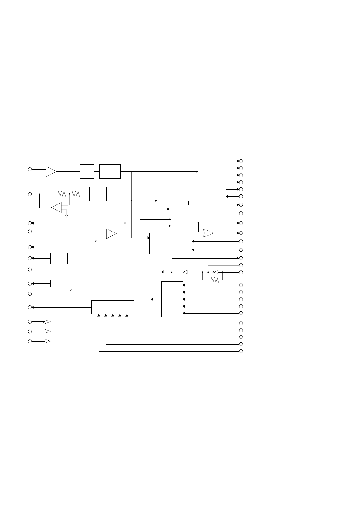
BLOCK DIAGRAM
DT1
DT2
DT3
DT4
SP
DTTIM
CP
CPW
CD
RD
TD
RS
CLK
X2
X1
MODE1
MODE2
MODE3
ICTA
ICTB
TEN
DTG1
DTG2
DTG3
DTG4
AIN
AOUT
GAT2
GAT1
MOD
VR1
VR2
SGO
SGC
DTO
PON
V
DD
GND
Mode
Select
&
Test
FSK Modem
Carrier
Detector
CPT
Detector
DTMF
Receiver
2765 Hz
BEF
PreLPF
Smooth
Voltage
Ref.
SG
DTMF
Generator
+
–
–
+
–
+
*
*
*
*
*
*
*
*
*
*
*
*
*
Power ON
+3 V
0 V
4 dB
Note)
DT1 to DT4 :
3-state outputs
* :
Input with
pull-up resistor
*
*
Page 3
¡ Semiconductor MSM7715
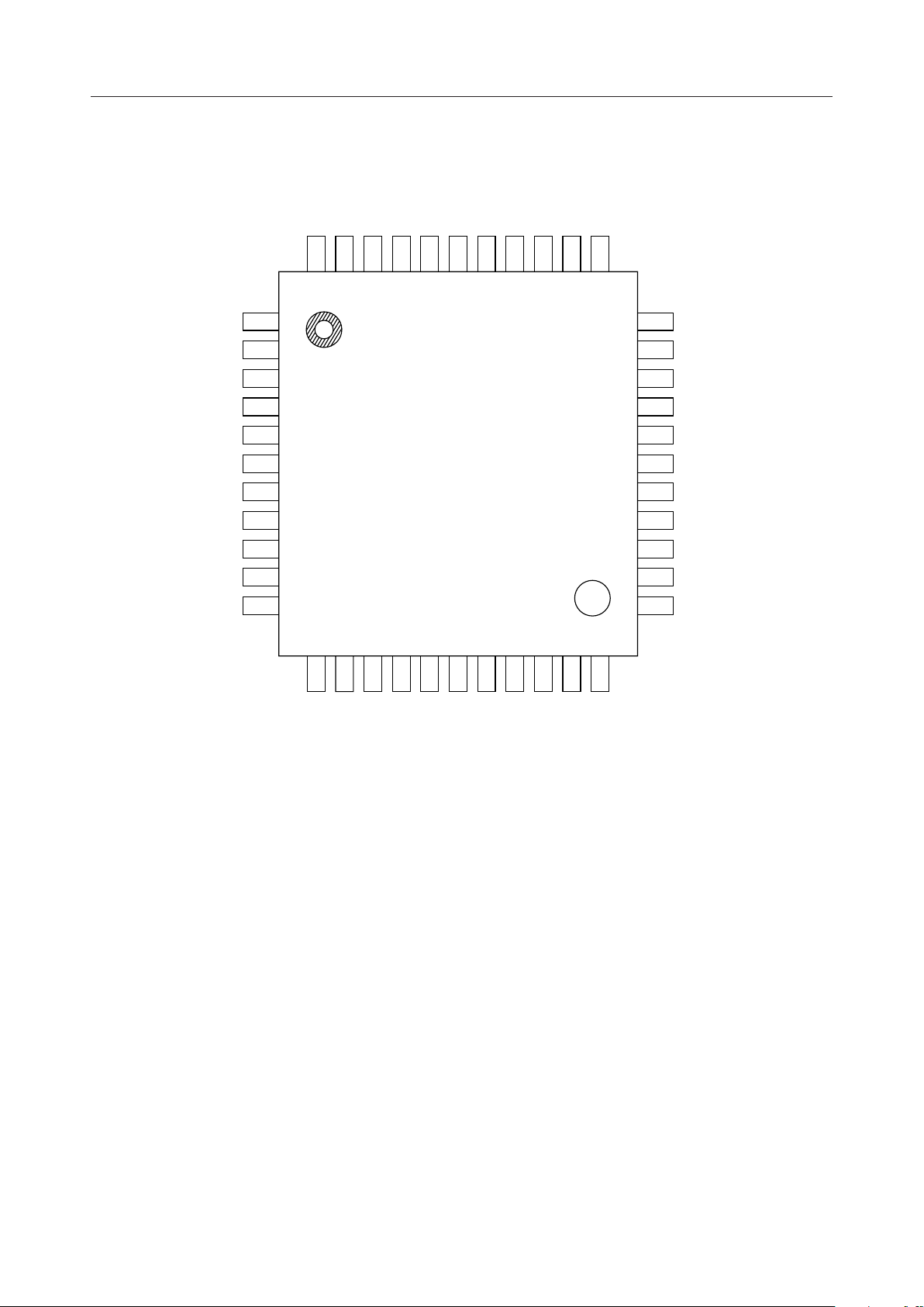
PIN CONFIGURATION (TOP VIEW)
DTG343DTG242DTG141GND40VR239VR138DTO37MOD36GAT235GAT134SGC
44
DTG4
TEN
TD
RS
CPW
ICTA
ICTB
DTTIM
MODE1
MODE2
MODE3
10
11
1
2
3
4
5
6
7
8
9
12
13X214NC15
X1
16RD17CD18CP19
CLK
DT120DT221DT322DT4
33
32
31
30
29
28
27
26
25
24
23
NC
SGO
AIN
NC
V
DD
NC
AOUT
NC
NC
PON
SP
NC : No connect pin
44-Pin Plastic QFP
3/21
Page 4

¡ Semiconductor MSM7715
PIN DESCRIPTION
Pin No. I/OName
DTG4
TEN 2
TD 3
RS 4
CPW 5
ICTA 6
ICTB 7
DTTIM 8
MODE1 9
MODE2 10
MODE3 11
X1 12
X2 13
CLK 15
Description
1
I*
Input for specifying the DTMF code to be sent.
Input for controlling output of the DTMF signal. (Transmit enable)
I*
DTG1 to DTG4 are latched at the falling edge of TEN and the DTMF signal is
output when “0” is input. See Fig. 2.
Input for data to be sent to the modem. Input the data string at a speed of 300 bps
I*
or lower.
Input for controlling the modem sending output. (Request to send)
I*
The sending signal is output when “0” is input.
Input for selecting the output waveform from the call progress tone detector.
When "1" is input, a rectangular wave that is synchronized with the input signal is
I*
output from the CP.
When "0" is input, presence of detected signal is output from the CP pin. See Fig.3.
Inputs for testing. Leave them open or connect them to V
I*
Input pin for controlling the detection timing of the DTMF receiver.
I*
When “0” is input, the high-speed detection mode is selected.
I*
Input for selecting the operation mode. See Table 1.
I
Input and output connected to the crystal oscillator. See “Oscillation Circuit” in
the Functional Description.
O
3.579545 MHz clock output
O
DD
.
RD 16
CD 17
CP 18
DT1 19
DT2 20
DT3 21
DT4 22
SP 23
PON 24
AOUT 27
Output for serial data received by the modem. It is held in the marked state
O
(“1”) when the carrier detector (CD) does not make detection.
Output for the carrier detector. “0” means detection, while “1” means
O
non-detection.
Output for call progress tone (CPT) detection. When the CPT is detected,
O
the waveform selected by the CPW pin is output. See Fig. 3.
Outputs for the code of the received DTMF signal. In a mode other than the
O
DTMF receiving mode, these pins are in a high-impedance state.
Output for presenting the DTMF signal receiving data. “1” means that the DTMF
O
signal is being received. Latch DT1 to DT4 at the rising edge of SP.
See Fig. 1.
Input for controlling power-on. When “1” is input, all lines of this device enter the
I*
power down state, and then the operation of each funciton stops and the receiver
timer is reset.
Analog signal output. The DTMF signal or modem sending signal is output.
O
4/21
Page 5
¡ Semiconductor MSM7715
Pin No. I/OName
V
DD
29
—
AIN 31 I
SGO 32 O
SGC 34
—
GAT1 35 I
GAT2 36 O
MOD 37 O
DTO 38 O
VR1 39 O
VR2 40 I
GND 41
—
DTG1 42
DTG2 43
DTG3 44
Description
Power supply. Supply +2.5V to 3.6V.
Input for the analog receiving signal.
Output for the signal ground voltage. The output voltage is 1/2 V
Connect a capacitor of 0.1 mF or more between SGO and GND.
Pin for connecting the capacitor of the signal ground voltage generating circuit.
Connect a capacitor of 1 mF or more between SGC and GND.
Input for the sending output level-adjusting amplifier.
Output for the sending output level-adjusting amplifier.
Output for the sending modem signal.
Output for the DTMF signal.
Output for the reference voltage generating circuit.
The potential difference between VR1 and SGO is approximately +0.75 V.
Input for external adjustment of the modem’s carrier detection level.
Ground.
Inputs for specifying the DTMF code to be sent.
I*
Data is latched at the falling edge of TEN.
DD
.
Note: Digital inputs that are pulled up internally by a high resistance.
5/21
Page 6
¡ Semiconductor MSM7715
ABSOLUTE MAXIMUM RATINGS
Parameter Condition UnitRating
Power Supply Voltage
Input Voltage
Storage Temperature
Symbol
V
DD
V
I
T
STG
Ta = 25°C
With respect to GND
—
RECOMMENDED OPERATING CONDITIONS
Parameter Min. Unit
Power Supply Voltage
Operating Temperature Range
Input Voltage
Input Clock Frequency
X1/X2 Load Capacitance
SGC Bypass Capacitance
SGO Bypass Capacitance
V
Bypass Capacitance
DD
Oscillation Frequency
Frequency Deviation
Temperature
Characteristics
V
DD
T
op
V
IH
V
IL
f
CLK
C1, C2
C3
C6
C5
—
—
—
Crystal
Equivalent Series
Resistance
—
ConditionSymbol Typ. Max.
—
—
—
Against 3.579545 MHz
—
—
— 0.1 — —
—
—
At 25°C ±5°C
At –40°C to +85°C
—
–0.3 to 7
–0.3 to VDD + 0.3
–65 to +150
2.5
3.0
–40
0.8 V
DD
0
–0.1
—
—
10
—
3.579545
–100
–50
—
—
—
—
—
12
—
—
—
—
V
V
°C
3.6
+85
V
DD
0.2 V
+0.1
—
1
—
V
°C
V
DD
%
pF
mF
—
MHz
—
+100
ppm
+50
90
W
Load Capacitance
—
—
—
16
—
pF
ELECTRICAL CHARACTERISTICS
DC Characteristics
= 2.5 V to 3.6 V, Ta = –40°C to +85°C)
(V
DD
Parameter Min. Unit
I
Power Supply Current
Input Current
*1
Output Voltage
*2
I
I
V
V
V
V
DD1
DD2
DDS
I
IH
I
IL
OH1
OL1
OH2
OL2
PON = "0"
V
= V
IH
DD
VIL = 0 V
CLK
C
£10 pF
L
Notes: *1 The following pins have an internal pull-up resistor. : DTG1 to DTG4, TEN, TD, RS,
CPW, ICTA, ICTB, DTTIM, MODE1 to MODE3, and PON
*2 RD, CD, CP, DT1 to DT4, and SP
ConditionSymbol Typ. Max.
Modem mode
DTMF mode
Power-downPON = "1"
—
—
—
–10
–50
V
*2
IOH = –100 mA
I
= 100 mA
OL
I
= –100 mA
OH
I
= 100 mA
OL
– 0.1
DD
0
0.9 V
0
DD
3
2.4
1
—
–10
—
—
—
—
6
5
20
10
10
V
DD
0.1
V
DD
0.1 V
mA
mA
V
DD
6/21
Page 7
¡ Semiconductor MSM7715
AC Characteristics (DTMF)
(
VDD = 2.5 V to 3.6 V, Ta = –40°C to +85°C)
Parameter Min. Unit
V
Transmit Level
Transmit Signal Level
Relative Value
V
V
DTTL
DTTH
DTDF
AOUT, R1 = R3
High-group tone/low-group tone
ConditionSymbol Typ. Max.
Low-group tone
High-group tone
–16.5
–15.5
0
–14.5
–13.5
–12.5
–11.5
1
2
dBm
*1
dB
Transmit Frequency
Deviation
Transmit Signal
Distortion Rate
DTG1 to DTG4 Input Data
Setup Time
DTG1 to DTG4 Input Data
Hold Time
Receive Detect Level
Receive Reject Level
Receive Frequency
Detect Band
Receive Frequency
Reject Band
Allowable Receive Level
Difference
Allowable Receive
Noise Level ratio
f
DDT
THD
t
SDT
t
HDT
V
DETDT
V
REJDT
f
DETDT
f
REJDT
V
TWIST
V
N/S
With respect to the nominal frequency
Harmonics/Fundamental frequency
DT
See Fig. 2.
See Fig. 2.
For each single tone
For each single tone
With respect to the nominal frequency
With respect to the nominal frequency
High-group tone/low-group tone
Noise (0.3 kHz to 3.4 kHz)
level/tone level
–1.5
—
250
250
–46
—
—
±3.8
–6
—
—
—
—
—
—
—
—
—
—
–12
+1.5
–23
—
—
–10
–60
±1.5
—
+6
—
%
dB
ns
dBm
*1
%
dB
Dial Tone Reject Ratio
Signal Repetition Time
Tone Time for Detect
Tone Time for No Detect
Output Delay Time
Interdigit Pause Time
Acceptable Drop Out Time
SP Delay Time
Output Trailing Edge
Delay Time
V
REJ400
t
t
t
t
t
t
t
G11
t
G12
t
G21
t
G22
t
t
t
t
t
SP1
t
SP2
t
t
D1
D2
C1
C2
S1
S2
P1
P2
B1
B2
380 Hz to 420 Hz
DTTIM = "1"
DTTIM = "0"
DTTIM = "1"
37
120
70
49
—
—
—
—
—
—
—
—
See Fig. 1
DTTIM = "0"
I1
I2
Normal
condition *2
Just after
mode change *3
DTTIM = "1"
DTTIM = "0"
DTTIM = "1"
DTTIM = "0"
DTTIM = "1"
DTTIM = "0"
DTTIM = "1"
DTTIM = "0"
DTTIM = "1"
DTTIM = "0"
DTTIM = "1"
DTTIM = "0"
> 80 ms
t
S
> 44 ms
t
S
DTTIM = "1"
DTTIM = "0"
34
—
—
30
20 42
30
21
—
—
6
1
21
15 27
—
—
—
45
32
4830 77
3520 62
—
—
—
—
8
1.7
29
21
—
24
9
57
ms
—
—
10
3
10
3
35
7/21
Page 8

¡ Semiconductor MSM7715
Note: *1 0 dBm = 0.775 Vrms (For all AC characteristics)
*2 "Normal condition" means that a DTMF signal appears after more than 20 ms after
setting DTMF receive mode.
*3 "Just after mode change" means that there is an input signal when the mode is
changed from DTMF transmit mode to DTMF receive mode. If there is an input
signal when power is turned on, see "DTMF mode setting procedure after power on
or after releasing power down mode".
AC Characteristics (Modem)
(
VDD = 2.5 V to 3.6 V, Ta = –40°C to +85°C)
Parameter Min. Unit
Modem Transmit Level
Signal Level Relative Value
Modem Transmit
Carrier Frequency
V
V
AOM
DM
f
OM
f
OS
f
AM
f
AS
Measured at AOUT pin, R1 = R2
Mark signal/space signal
Originate mode
Answer mode
Transmit Signal Output Deray
Time
Modem Receive Signal Level
Carrier Detection (CD)
Signal Level
CD Level Hysteresis
CD Delay Time
CD Hold Time
t
ADD
V
AIM
V
V
OFF
V
HYS
t
CDD1
t
CDD2
t
CDH1
t
CDH2
TD Æ AOUT
Measured at AIN. FSK modulation signal
Answer mode : 1080 Hz
ON
Originate mode : 1750 Hz
VR2 open at AIN pin
OFF Æ –6 dBm
OFF Æ –40 dBm
–6 dBm Æ OFF
–40 dBm Æ OFF
ConditionSymbol Typ. Max.
–11 dBm
–9 –7
–1.5 0 1.5
Mark, TD = "1"
Space, TD = "0"
Mark, TD = "1"
Space, TD = "0"
976 980 984
1176 1180 1184
1646 1650 1654
1846 1850 1854
— 3.5 —
–48 *1 — –6
OFFÆON
ONÆOFF
— –44 –42
–48 –46 —
—2—
—8—
51422
20 31 40
—23—
dB
Hz
ms
dBm
dB
ms
Demodulated Data Bias
Distortion
NRTS Signal Versus
Modem Receive Signal
Allowable Level Ratio
Receive data output Delay
Time
D
V
t
RDD
300 bps,1 : 1 pattern
BS
V
/V receive modem signal
NR
NRTS
NRTS : 2765 Hz ±30 Hz
AIN Æ RD
— — ±10
——–2
—5—
*1 When the carrier detector does not detect (CD="1"), RD is fixed to "1".
AC Characteristics (Call progress tone detector)
(
VDD = 2.5 V to 3.6 V, Ta = –40°C to +85°C)
Parameter Min. Unit
CPT Detect Level
CPT Non-Detect Level
CPT Detect Frequency
CPT Non-Detect Frequency
CPT Detect Delay Time
CPT Detect Hold Time
V
DETCP
V
REJCP
f
DETCP
f
REJCP
t
DELCP
t
HOLCP
400 Hz
400 Hz
See Fig. 3.
See Fig. 3.
ConditionSymbol Typ. Max.
–40 dBm
— dBm— –60
380 Hz— 420
500
— — 300
—
—
—ms20 —
—ms15 —
%
dB
ms
—–6
——
Hz
8/21
Page 9

¡ Semiconductor MSM7715
AC Characteristics
(
VDD = 2.5 V to 3.6 V, Ta = –40°C to +85°C)
Parameter Min. Unit
Transmit Signal Output Level
Output Load Resistance
Output Impedance
Input Impedance
Output DC Potential
Out-of-band Output Noise
V
R
R
R
V
V
AOUT
R
LVR1
LAO
OX
R
V
SG
DCAO
REF
V
V
V
AOUT
MOD, DTO, GAT2
LX
Resistor between VR1 and SGO
AOUT
AOUT, MOD, DTO, GAT2, VR1, SGO
GAT1, AIN
AI
SGO
AOUT
Potential difference between VR1 and SGO
S1
Measured at AOUT
S2
R1= 30 kW
C4 = 680 pF
S3
ConditionSymbol Typ. Max.
—
20
40
30
—
—
VDD/2–0.1
—
—
—
—
100
10
VDD/2
1.1
—
—
—
—
—
VDD/2+0.1
—VDD/2 —
0.7 0.75 0.8
4 kHz to 8 kHz
8 kHz to 12 kHz
— — –45
— — –65
every 4 kHz
bandwidth of
— –70 –60
12 kHz or more
Vp-p
kW
W
MW
V
dBm
9/21
Page 10

¡ Semiconductor MSM7715
TIMING DIAGRAM
When DTMF is received
t
C
t
B
AIN signal
DT1 to 4
t
I
t
G
t
S
t
P
t
D
SP
t
S
t
I
t
P
t
B
t
SP
t
C
t
G1n
t
D
t
SP
Figure 1 DTMF Receive Timing
: Tone time for detect
When the input signal duration is tS or more, receiving is normally done.
: Tone time for no detect
When the input signal duration is tI or less, this input signal is ignored and DT1 to
DT4 and SP is not output.
: Interdigit pause time
When there is no input signal for tP or more, DT1 to DT4 and SP are reset.
: Acceptable drop out time
DT1 to DT4 and SP are not reset even though a no-signal state for tB or less
(momentary no-signal) occurs during signal receiving. The tB is applicable while
the received signals are output. (SP="1")
: SP delay time
Against the DT1 to DT4 output, SP is output after a delay of tSP. Therefore, latch DT1
to DT4 at the rising edge of SP.
: Signal repetition time
For normal receiving, set the signal repetition time to tC or more.
: Output delay time (n: 1 or 2)
Against the appearance of the input signal, DT1 to DT4 are outputs after a delay of
t
.
G1n
: Output trailing edge delay time
Against the stop of the input signal, DT1 to DT4 and SP stop outputting after a delay
of tD.
10/21
Page 11

¡ Semiconductor MSM7715
When the DTMF tone is sent
TEN
DTG1
DTG2
DTG3
DTG4
DTO
t
SDT
t
HDT
941 Hz + 1447 Hz
Figure 2 DTMF Transmit Timing
When the call progress tone (CPT) is detected
AIN
CP CPW = "1"
CP
CPW = "0"
t
DELCP
Figure 3 Call Progress Tone Detect Timing
400 Hz
t
HOLCP
11/21
Page 12

¡ Semiconductor MSM7715
FUNCTIONAL DESCRIPTION
Oscillation circuit
Connect a 3.579545 MHz crystal resonator between X1 and X2. If the load capacitance of the
crystal resonator is 16 pF, connect a 12 pF capacitor between X1 and GND and between X2 and
GND.
When an external clock is used, input the external clock to X2 via a 200 pF capacitor and leave
X1 open.
C1
X1
X2
C2
3.579545 MHz
X1
X2
3.579545 MHz
Figure 4 Connection of
the Crystal Resonator
Figure 5 Connection of
the External Clock
Signal ground
Connect a capacitor of 1 mF between SGC and GND. Do not connect anything other than this
capacitor to the SGC pin.
SGO can also be used as the reference voltage for the peripheral circuit. A capacitor of 0.1 mF or
more should be connected between SGO and GND.
To the
peripherals
SGC
C3
SGO
C6
–
SG voltage
+
generating
circuit
+
–
+
–
To the internal
circuit
Figure 6 Signal Ground
Digital input pin
The digital input pin contains a pull-up resistor. Therefore, supply the VIH voltage (VDD) to this
pin or open this pin to input "1". To input "0", supply the VIL voltage (GND) to this pin.
Upon power down (PON = "1"), this pull-up goes into a high-impedance state. Therefore, current
is not affected upon power down even though the VIL voltage remains connected to the digital
input pin.
12/21
Page 13

¡ Semiconductor MSM7715
Operation mode selection
By setting the MODE1 to MODE3 pins, an operation mode can be selected (see Table 1). The call
progress tone detector (CPT DET.) can be operated in the DTMF signal transmit mode and
modem mode. However, since the carrier detector is also used for the call progress tone detector,
only rectangular waveform output is available in modem mode. Set CPW = "1" when activating
the call progress tone detector in a modem mode.
Table 1 Operation Mode Table
MODE
2
31
000
010
001
011
100
110
101
111
DTMF mode
Modem
mode
Operation Mode
DTMF signal transmit
DTMF signal receive
Normal
operation
Test
mode
Originate (O)
Answer (A)
Analog loopback
(ALB)
Remote digital
loopback (RDLB)
O
A
O
A
DTMF
GEN.
*
DTMF
REC.
Functional Block
FSK
MODEM
*
*
*
*
*
*
*
CPT DET.
CPW = "1"
*
*
*
*
*
*
*
CPW = "0"
*
* means active.
Note: The carrier detecor may malfunction within 40 ms after the operating mode is changed
from the DTMF or power down mode to the modem mode.
Therefore, ignore an output signal from CD and RD during this period of time.
DTMF mode setting procedure after power-on or after releasing power-down mode
The following is a recommendable procedure to use DTMF mode after power-on or after
releasing power-down mode.
(1) Put power-on or release power-down mode.
(2) Set DTMF signal transmit mode. PON="0", TEN="1"
(3) Wait more than 20 ms, VDD must be more than 2.5 V after this wait time.
(4-1) In the case of DTMF receive, set DTMF signal to receive mode.
(4-2) In the case of DTMF transmit, it is possible control transmit enable (TEN).
Modem mode setting procedure after power-on
The following is a recommendable procedure to use Modem mode after power-on.
(1) Power on.
(2) Set PON="1", TEN="1" and RS="1". Set mode to be used.
(3) More than 200 ms after VDD becomes more than 2 V, set PON="0".
(4) Wait more than 20 ms. VDD must be more than 2.5 V after this wait time.
(5) It is possible to control transmit output. Ignore an output signal from CD and RD of
more than 40 ms which includes the wait time of term (4).
13/21
Page 14

¡ Semiconductor MSM7715
Modem signal flow
Figure 7 shows the signal flow during normal modem operation.
RD
TD
Received data
Transmitted data
Line
AIN
AOUT
Receive filter Demodulator
Transmit filter Modulator
Figure 7 Signal Flow in Normal Operation
The MSM7715 uses the analog loopback test (ALB) mode and remote digital loopback test
(RDLB) mode as the modem testing functions. In these test modes, the signal flow shown in
Figure 8 is used. O (originate)/A (answer) in the test mode is the expression based on the
modulator side. In ALB mode, the transmit analog signal is input to the demodulator and can
be monitored as RD. In RDLB mode, the modem is configured as the remote modem in the RDL
test mode.
Data from the other modem that requested for RDL is returned to the other modem as a result
of echo-back.
AIN
Receive filter Demodulator
RD
Received data
[ALB]
[RDLB]
AOUT
AIN
AOUT
TD
Transmit filter Modulator
Receive filter Demodulator
Transmit filter Modulator
RD
TD
Figure 8 Signal Flow in Test Mode
Transmitted data
Received data
Transmitted data
14/21
Page 15

¡ Semiconductor MSM7715
DTMF signal code
Sixteen types of DTMF transmit signals can be set by using DTG1 to DTG4. Also, sixteen types
of DTMF receive signals can be monitored by using DT1 to DT4. Table 2 shows the DTMF signal
codes.
Table 2 DTMF Signal Codes
Button
Low-group signal (Hz)
697
**10001
**20010
**30011
**A1101
770 852 941 1209 1336 1477 1633
**40100
**50101
**60110
**70111
**81000
**91001
**01010
***1011
**#1100
**B1110
**C1111
**D0000
High-group signal (Hz)
DT4
DTG4
DT3
DTG3
DT2
DTG2
DT1
DTG1
15/21
Page 16

¡ Semiconductor MSM7715
Microcontroller interface
By externally connecting DT1 to DT4 and DTG1 to DTG4 respectively, a 4-bit bus can be
configured (Fig 9).
In DTMF signal transmit mode, DT1 to DT4 enter a high-impedance state and this 4-bit line is
used to set the DTMF code against DTG1 to DTG4. The bus data is latched at the falling edge of
TEN.
In DTMF signal receive mode, DT1 to DT4 enter an output state. The 4-bit bus line is used as the
output of the DTMF code from DT1 to DT4 to the microcontroller. Latch this bus data at the rising
edge of SP.
In modem mode, DT1 to DT4 enter a high-impedance state. This 4-bit bus line is pulled up by
the pull-up resistor in DTG1 to DTG4.
In power-down mode (PON = "1"), DT1 to DT4 enter a high-impedance state. Since the pull-up
resistors in DTG1 to DTG4 also enter a high-impedance state, potential of this 4-bit bus line
becomes unstable from the MSM7715.
Microcontroller
DT1
DT2
DTMF Receiver
DT3
DT4
DTG1
DTG2
DTMF Generator
DTG3
DTG4
Figure 9 Microcontroller Interface Example
16/21
Page 17

¡ Semiconductor MSM7715
Setting the transmit signal level
4dB
VAO
AOUT
GAT2
RC-LPF
+
–
C4
R2
R3
R1
GAT1
DTO
MOD
DTMF
Generator
Modulator
R1, R2, R3 ≥ 20 kW, R1 £ R2, R1 £ R3
Figure 10 Setting the Transmit Signal Level
The modem’s modulated analog signal and DTMF signal are not transmitted at the same time.
The signal to be transmitted is determined by the selected operation mode. This device provides
the pins for individual setting of transmit signal levels.
V
V
: Level of the modem signal at the AOUT pin when R1 = R2 (dBm)
AOM
: Level of the DTMF signal at the AOUT pin when R1 = R3 (dBm)
AODT
When external resistors (R1, R2, R3) are changed, the signal level at AOUT is as follows:
VAO (modem) = 20 ¥ log (R1/R2) + V
VAO (DTMF) = 20 ¥ log (R1/R3) + V
AOM
AODT
However, to avoid distorted output, R1 ≤ R2 and R1 ≤ R3 are needed. In circuit design, R1 = R2
or R1 = R3 with 5% tolerance is permitted.
C4 is a component in the first order LPF for suppressing the out-of-band output noise. Select a
value C4 in such a way that cutoff frequency FC determined by R1 and C4 will be approximately
8 kHz.
C4 = 1/ (2p ¥ R1 ¥ FC)
17/21
Page 18

¡ Semiconductor MSM7715
External adjustment of the carrier detection level
VR1
R4
R5
11
12
r
VR2
SG
6
1
VREF
r
2
r
: 300 kW, r2 : 600 kW
1
COMP
R4 + R5 ≥ 20 kW
Figure 11 External Adjustment of the Carrier Detection Level
The carrier detection level is determined by the resistance ratio between the MSM7715's internal
resistors r1 and r2, unless external resistors R4 and R5 are connected.
By connecting external resistors R4 and R5, the detection level can be adjusted. However, the
width of hysteresis cannot be changed.
Ra = R4 ¥ r1/(R4 + r1), Parallel-connected resistance of R4 and r
Rb = R5 ¥ r2/(R5 + r2), Parallel-connected resistance of R5 and r
1
2
VON = 20 ¥ log (Rb/(Ra + Rb)) –40.5 (dBm)
V
= 20 ¥ log (Rb/(Ra + Rb)) –42.5 (dBm)
OFF
Caution: r1 and r2 may vary in similar proportions over a 0.5 to 2.0 ¥ range, due to the lot
variation and temperature variation.
18/21
Page 19

¡ Semiconductor MSM7715
Analog Interface
C7
4 dB
r
AIN
SGO
4
r
3
–
+
–
+
SG
V
T
V
R
Line
600 W : 600 W
R9
–
+
AMP2
R11 R12
R8
R10
600 W
R7
AMP1
R13
C8
–
+
R6
R14
–
+
R15≥60 kW
C9
R15
AOUT
Figure 12 Analog Interface Circuit Example
When R1 = R2 in the modem mode, the AOUT output level is at its maximum value of about –9
dBm. When R1 = R3 in DTMF mode, the AOUT output level is at its maximum value of –11 dBm
(sum of the low group and high group). To increase the transmit output level in the line to a high
level, use an external amplifier (AMP1).
The receive signal levels can be adjusted by the values of R13 and R14.
Clock noise of about –70 dBm will be generated from AOUT as out-of-band noise. (Clock noise
has a frequency of 27.965 kHz and its odd harmonics.) The clock noise level is nearly always
constant even if the output level of AOUT is lowered by varying the values of resistors R1 to R3
that are connected to GAT1, GAT2, DTO, and MOD. Therefore, to suppress this noise output to
the line, build a LPF at the AMP1. Note, however, that setting the cutoff frequency of the LPF
too low affects the output signal level.
Note that too large a time constant determined by the values of C9 and R15 allows the longer time
required for reaching a stable DC level, which may result in the violation of specification for the
DTMF signal receive output delay time.
Example: R15=100 kW, C9=0.022 mF.
Larger circuit-return levels of the transmit signal to the AIN pin can cause receive data errors.
If the line impedance is equal to the R10 impedance, R8=R9 can not induce the circuit-return
levels of the transmit signal to the AIN pin.
The peripheral circuits should be designed so that the circuit-return level, including variations
of the line impedance, of the transmit signal to the AIN pin is –9 dBm or less.
19/21
Page 20

¡ Semiconductor MSM7715
APPLICATION CIRCUIT
Line
R9
R10
–
+
C4
C3
R1
R2
R3
R14
SGC
GAT1
GAT2
MOD
DTO
VR1
VR2
GND
DTG1
DTG2
DTG3
R13
R15
C6
C9
–
+
R7
AIN
SGO
DTG4
TENTDRS
C5
+
–
DD
V
R8
C7
–
+
R6
Positive Supply
C8
PON
AOUT
CPW
ICTA
ICTB
SP
DTTIM
MODE1
DT4
DT3
DT2
DT1
CP
CD
RD
CLK
X2
X1
MODE2
MODE3
R11
C2
C1
R12
Microcontroller
20/21
Page 21

¡ Semiconductor MSM7715
PACKAGE DIMENSIONS
(Unit : mm)
QFP44-P-910-0.80-2K
Mirror finish
Package material
Lead frame material
Pin treatment
Solder plate thickness
Package weight (g)
Epoxy resin
42 alloy
Solder plating
5 mm or more
0.41 TYP.
Notes for Mounting the Surface Mount Type Package
The SOP, QFP, TSOP, SOJ, QFJ (PLCC), SHP and BGA are surface mount type packages, which
are very susceptible to heat in reflow mounting and humidity absorbed in storage.
Therefore, before you perform reflow mounting, contact Oki’s responsible sales person for the
product name, package name, pin number, package code and desired mounting conditions
(reflow method, temperature and times).
21/21
 Loading...