

Page 1

E2U0044-16-X2
¡ Semiconductor MSM7708-02
¡ Semiconductor
This version: Jan. 1998
Previous version: Nov. 1996
MSM7708-02
Serial Register Interface ADPCM CODEC for Telephone Recording
GENERAL DESCRIPTION
The MSM7708-02 is a CMOS IC developed for applying to PHS (Personal Handyphone System).
This device provides a CODEC function which performs transcoding between the voice band
analog signal and 32 kbps ADPCM data. It also provides a serial register interface function for
telephone call recording.
Provided with such functions as DTMF tone and several kinds of tone generation, transmit/
receive data mute and gain control, side-tone pass, and voice/silence detection, the MSM770802 is best suited for PHS handsets.
FEATURES
• Single 3 V power supply operation (VDD: 2.7 V to 3.6 V)
• Low power consumption
When system is operating: 6 mA typ.
When powered down: 0.02 mA typ.
(ADPCM CODEC)
• ADPCM: ITU-T Recommendations G.721 (32 kbps)
• Transmit/receive full duplex capability
• PCM interface code format: m-law or A-law selectable
• Serial ADPCM and PCM transmission rate: 64 kbps to 2,048 kbps
• Transmit/receive mute function; transmit/receive programmable gain setting
• Side tone generator (8-step level adjustment)
• Built-in DTMF tone, ringing tone, and various tone generators
• Built-in VOX function
(Serial Register Interface)
• Interface for a serial register: 1 Mb (MSM63V89C), 4 Mb (MSM6684), 8 Mb (MSM6685)
• Interface for a serial voice ROM: 1 Mb (MSM6595A), 2 Mb (MSM6596A), 3 Mb (MSM6597A)
• Maximum recording time: 32 s (1 Mb), 128 s (4 Mb), 256 s (8 Mb)
• Maximum recording channels: 32 ch
• Playback data transmit/receive selectable
• Package:
64-pin plastic TQFP (TQFP64-P-1010-0.50-K) (Product name : MSM7708-02TS-K)
1/38
Page 2
¡ Semiconductor MSM7708-02
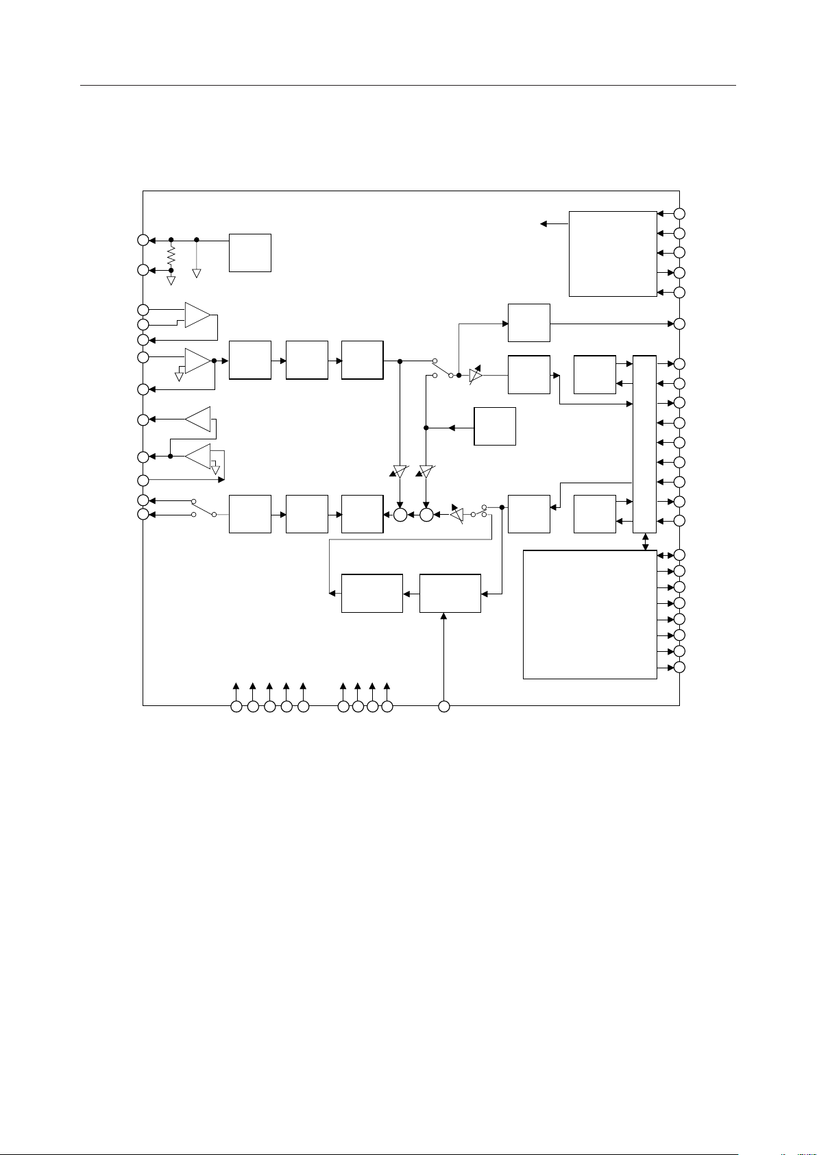
BLOCK DIAGRAM
SGR
SGT
AIN1–
AIN1+
GSX1
AIN2
GSX2
AOUT+
AOUT–
PWI
VFRO
SAO
T
T
1.2 kW
1.2 kW
To various units
EXCK
DEN
VREF
MCU
Interface
DIN
DOUT
RESET
–
+
–
+
RC
Filter
A/D
Converter
BPF
ATT
–1
–
+
ATT
Voice
Detect
Compan-
DTMF
/Tone
Generator
der
ADPCM
Coder
P/S
&
S/P
VOXO
IS
PCMSI
PCMSO
XSYNC
BCLK
RSYNC
PCMRI
RC
Filter
D/A
Converter
LPF
+ +
ATT
Expan-
der
ADPCM
Decoder
PCMRO
IR
DIO
WE
Noise
Generator
Power
Detect
Serial
Register
Controller
SAD
SAS
TAS
RWCK
CS1
To various units
To receive unit
CS2
V
DD
DG
AG
PDN
MCK
MLV0
MLV1
MLV2
MUTE
VOXI
2/38
Page 3
¡ Semiconductor MSM7708-02
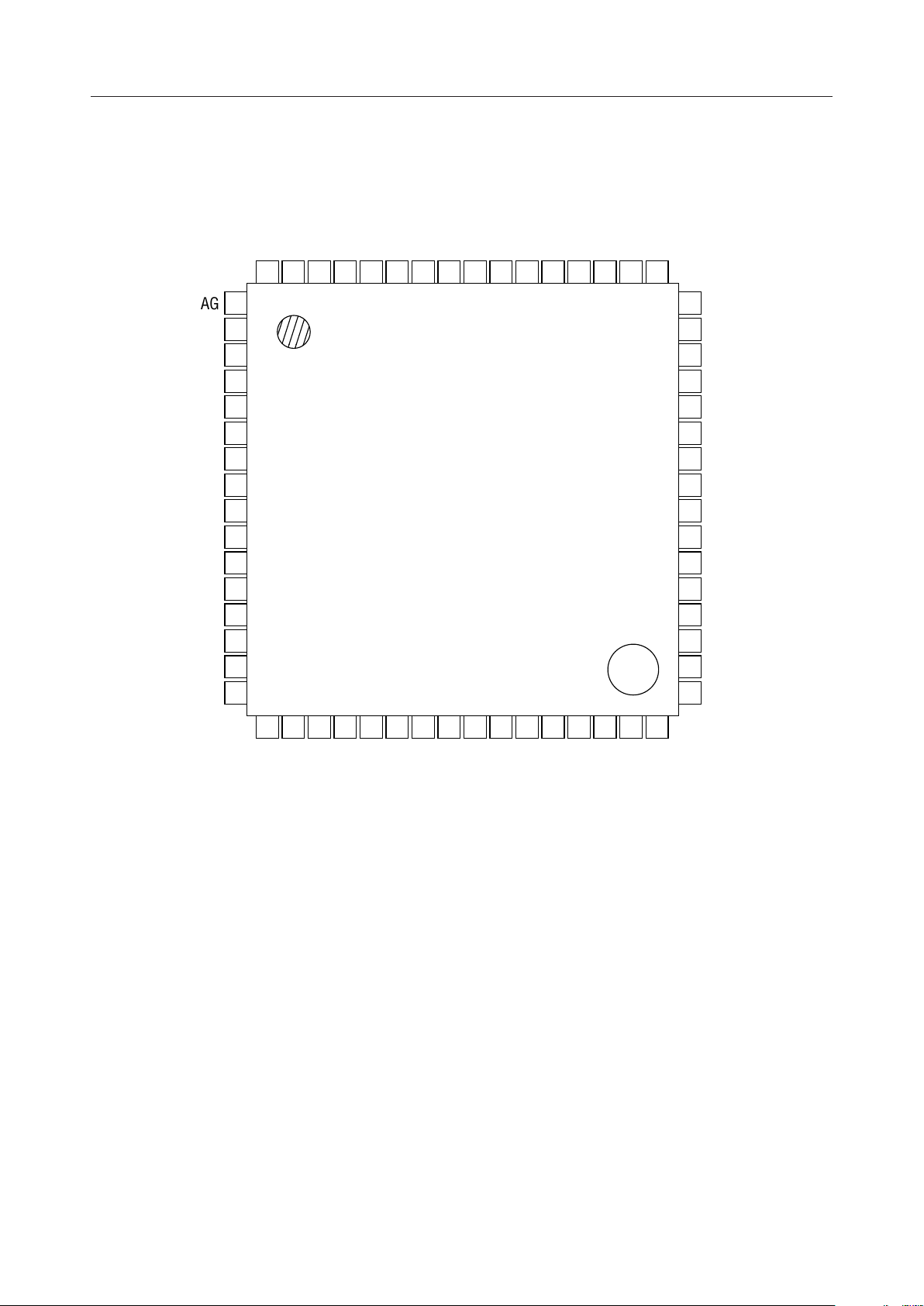
PIN CONFIGURATION (TOP VIEW)
NC
DIOWENC
64
63
62
61
SAD
60
SAS
59
TAS
58
RWCK
CS1
57
56
CS2NCBCLK
55
54
53
RSYNC
XSYNCNCDG
52
51
50
49
AG
NC
SAO
NC
NC
VFRO
PWI
AOUT–
AOUT+
SGR
NC
SGT
AIN1–
GSX1
AIN+
NC
10
11
12
13
14
15
16
32
NC
48
47
46
45
44
43
42
41
40
39
38
37
36
35
34
33
NC
PCMSO
PCMSI
NC
IS
IR
NC
PCMRO
PCMRI
NC
MCK
PDN
RESET
DOUT
DIN
NC
1
2
3
4
5
6
7
8
9
17
18
19
20
21
22
23
24
25
26
27
28
29
30
31
NC
GSX2
AIN2
V
DD
NC
MLV2
MLV1
MLV0
NC
MUTE
VOXI
VOXO
NC
DEN
EXCK
NC : No connect pin
64-Pin Plastic TQFP
3/38
Page 4

¡ Semiconductor MSM7708-02
PIN DESCRIPTIONS
Pin
1
2
3
4
5
6
7
8
9
10
11
12
13
14
15
16
17
18
19
20
21
22
23
24
25
26
27
28
29
30
31
32
33
34
35
36
37
38
39
40 I Receive side PCM signal input
Symbol
AG
NC
SAO
NC
NC
VFRO
PWI
AOUT–
AOUT+
SGR
NC
SGT
AIN1–
GSX1
AIN1+
NC
NC
GSX2
AIN2
V
DD
NC
MLV2
MLV1
MLV0
MUTE
NC
VOXI
VOXO
NC
DEN
EXCK
NC
NC
DIN
DOUT
RESET
PDN
MCK
NC
PCMRI
Type Description
I Analog ground
— No connection
O Receive side sounder amplifier output
— No connection
— No connection
O Receive side voice output
I Receive side voice amplifier input
O Receive side voice amplifier output (–)
O Receive side voice amplifier output (+)
O Receive side analog signal ground
— No connection
O Transmit side analog signal ground
I Transmit side amplifier 1 inverting input
O Transmit side amplifier 1 output
I Transmit side amplifier 1 non-inverting input
— No connection
— No connection
O Transmit side amplifier 2 output
I Transmit side amplifier 2 inverting input
I Power supply
— No connection
I Receive side voice path mute level set
I Receive side voice path mute level set
I Receive side voice path mute level set
I Receive side voice path mute enable signal input
— No connection
I Receive side voice/silence detect function input
O Transmit side voice/silence detect function output
— No connection
I Enable signal input for control register
I Clock signal input for control register
— No connection
— No connection
I Address and data input for control
O Data output for control register
I RESET control input for control register
I Power down control input
I Master clock input
— No connection
4/38
Page 5

¡ Semiconductor MSM7708-02
PIN DESCRIPTIONS (Continued)
Pin
41
42
43
44
45
46
47
48
49
50
51
52
53
54
55
56
57
58
59
60
61
62
63
64 — No connection
Symbol
PCMRO
NC
IR
IS
NC
PCMSI
PCMSO
NC
DG
NC
XSYNC
RSYNC
BCLK
NC
CS2
CS1
RWCK
TAS
SAS
SAD
NC
WE
DIO
NC
Type Description
O Receive side PCM signal output
— No connection
I Receive side ADPCM signal input
O Transmit side ADPCM signal output
— No connection
I Transmit side PCM signal input
O Transmit side PCM signal output
— No connection
I Digital ground
— No connection
I Transmit side PCM and ADPCM data sync signal input
I Receive side PCM and ADPCM data sync signal input
I PCM and ADPCM data shift clock input
— No connection
O Voice ROM chip select output
O Serial register chip select output
O Serial register data clock output
O Serial register transfer address-strobe output
O Serial register address-strobe output
O Serial register address data output
— No connection
O Serial register write enable output
I/O Serial register data input/output
5/38
Page 6

¡ Semiconductor MSM7708-02
PIN AND FUNCTIONAL DESCRIPTIONS
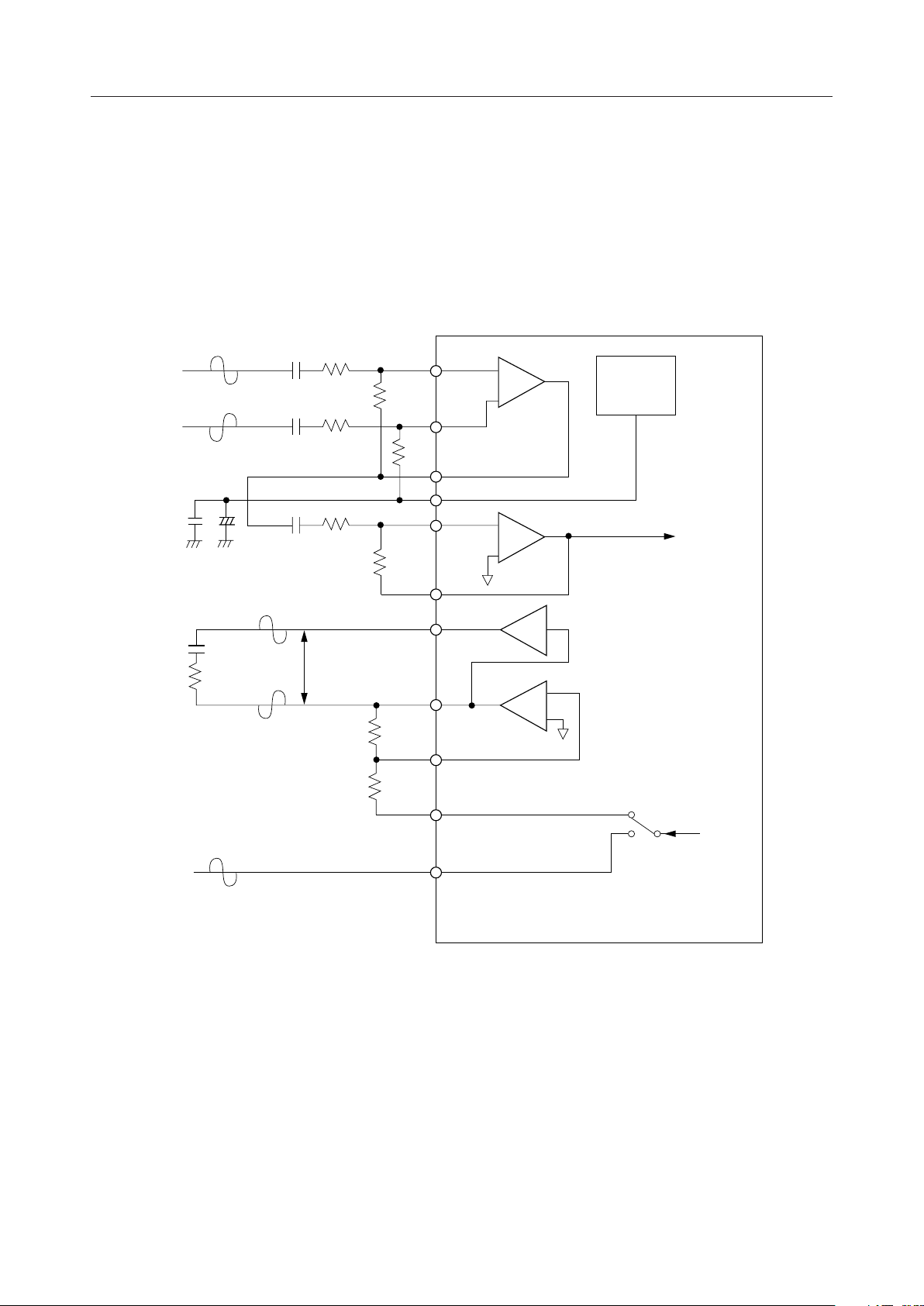
AIN1+, AIN1-, AIN2, GSX1, GSX2
The transmit analog input and the output for transmit gain adjustment.
The pin AIN1– (AIN2) connects to inverting input of the internal transmit amplifier, and the pin
AIN1+ connects to non-inverting input of the internal transmit amplifier. The pin GSX1 (GSX2)
connects to output of the internal transmit amplifier. Gain adjustment should be referred to
Fig. 1.
VFRO, AOUT+, AOUT-, PWI
Used for the receive analog output and the output for receive gain adjustment.
VFRO is an output of the receive filter. AOUT+ and AOUT– are differential analog signal outputs
which can directly drive ZL = 350 W+120 nF or the 1.2 kW load. Gain adjustment should be
referred to Fig. 1.
These outputs are in high impedance state during power down.
6/38
Page 7
¡ Semiconductor MSM7708-02
SAO
Differential analog output for a sounder.
Variable tones including "Audio sound", "DTMF tone", "S tone", "F tone", and "R tone", and
telephone call signals can be output to either VFRO pin or SAO pin by CR0 - B1 of the control
register. These output pins are in the high impedance state during power down.
Vi
Differential analog input signal
+
–
Z
= 120 nF
L
+ 350 W
Transmit gain : (V
= (R2/R1) ¥ (R4/R3)
Receive gain : (V
= 2 ¥ (R6/R5)
C1
C1 R1
C2
GSX2/VI
R1
R3
Analog output signal
Vo
)
/V
)
O
VFRO
R6
R5
R2
R4
R2
AIN1–
AIN1+
GSX1
SGT
AIN2
GSX2
AOUT+
AOUT–
PWI
VFRO
–
+
–
+
–1
–
+
Reference
voltage
generator
to ENCODER
from
DECODER
Sounder output signal
Figure 1 Analog Interface
SAO
7/38
Page 8

¡ Semiconductor MSM7708-02
SGT, SGR
Outputs of the analog signal ground voltage.
SGT outputs the analog signal ground voltage of the transmit system, and SGR outputs the same
for the receive system. The output voltage value is approximately 1.4 V. Connect bypass 10 mF
and 0.1 mF (ceramic type) capacitors between these pins and the AG pin. To reduce the response
time of the receiver power on, it is recommended to apply 1 mF and 0.1 mF bypass capacitors.
During power down, the output changes to 0 V.
V
DD
Power supply.
DG, AG
Ground.
DG is the digital system ground. AG is the analog system ground. Since DG and AG are separated
in the device, connect them as close as possible on the circuit board.
PDN
Power down control input.
When set to a digital "0", the system changes to the power down state and control register is not
reset. Since the power down mode is controlled by CRC0 - B5 of the control register ORed with
the signal from the PDN pin, set CRC0 - B5 to digital "0" when using this pin.
RESET
Reset control input of the CODEC control register.
When set to digital "0," each bit of the control register is reset and the internal circuit changes to
the power down state. During normal operation, set this pin to digital "1".
MCK
Master clock input.
The clock frequency is 19.2 MHz. MCK can be asynchronous with XSYNC, RSYNC, and BCLK.
8/38
Page 9

¡ Semiconductor MSM7708-02
PCMSO
Transmit PCM data output.
This PCM output signal is output from MSB synchronously with the rising edge of BCLK and
XSYNC.
PCMSI
Transmit PCM data input.
This signal is converted to the ADPCM data. The PCM signal is shifted in on the falling edge of
BCLK. Normally, this pin is connected to PCMSO.
PCMRO
Receive PCM data output.
This PCM signal is the output signal after ADPCM decoder processing. This signal is serially
output from MSB synchronously with the rising edge of BCLK and RSYNC.
PCMRI
Receive PCM data input.
This PCM input signal is shifted in on the rising edge of BCLK and is input from MSB. Normally,
this pin is connected to PCMRO.
IS
Transmit ADPCM signal output.
This signal is the output signal after ADPCM encoding, and is serially output from MSB
synchronously with the rising edge of BCLK and XSYNC. This pin is an open drain output which
remains in a high impedence state during power down. It requires pull-up resistor.
IR
Receive ADPCM signal input.
This input signal is shifted in serially on the rising edge of BCLK synchronously with RSYNC and
is input from MSB.
BCLK
Shift clock input for the PCM data (PCMSO, PCMSI, PCMRO, PCMRI) and the ADPCM data(IS,
IR) . The frequency is in the 64 kHz to 2048 kHz range.
XSYNC
8 kHz synchronous signal input for transmit PCM and ADPCM data.
This signal should be synchronized with BCLK. XSYNC is used for indicating the MSB of the
transmit serial PCM and ADPCM data stream.
RSYNC
8 kHz synchronous signal input for receive PCM and ADPCM data.
This signal should be synchronized with BCLK signal. RSYNC is used for indicating the MSB
of the receive serial PCM and ADPCM data stream.
9/38
Page 10
¡ Semiconductor MSM7708-02
(b)
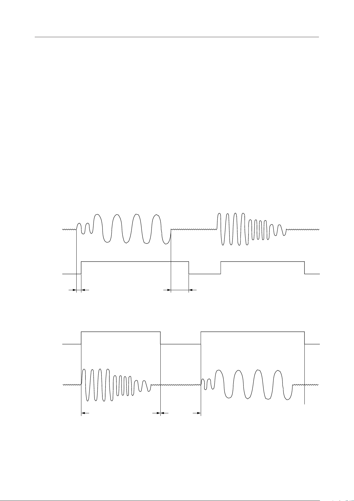
VOXO
Transmit side voice/silence detect signal output.
This output is valid when CR6 - B7 is set to "1". VOXO shows the presence or absence of the
transmit voice signal by detecting the signal. "1" and "0" set to this pin correspond to the presence
and the absence, respectively. This result also appears at the register data CR7 - B7. The signal
detect threshold is set by the control register CR6 - B6, B5. When control register CR0 - B6 is set
to "1" and VOXI input is "1" during the voice detection (VOXO = "1"), receive signal is
automatically suppressed by 6 dB.
VOXI
Receive side voice/silence detect signal input.
This output is valid when CR6 - B7 is set to "1". A "1" level at VOXI indicates the presence of voice
signal, in which case the decoder block processes normal receive signal and the voice signal
appears at analog output pins. A "0" level indicates the absence of voice signal, in which case the
background noise generated in this device is transferred to the analog output pins. The
background noise amplitude is set by the control register CR6 - B1, B0. Since this signal is ORed
with the register CR6 - B3, set the control register CR6 - B3 to "0" when using this pin. When
control register CR0 - B6 is set to "1" and VOXI input is "1" during the voice detection (VOXO =
"1") receive signal is automatically suppressed by 6 dB.
Input voice signal
GSX2
pin
VOXO pin
VOXI pin
Regenerated voice
VFRO
pin
Voice Silence Voice
Voice Detection Time
T
VXON
(a) Transmission Side Voice/Silence Detect Function Timing Diagram
Voice Silence Voice
Silence Detection Time
(Hangover Time) T
VXOFF
Regenerated Voice Signal
Generation Time
Receive Side Voice/Silence Detect Function Timing Diagram
Internal Background
Noise Generation Time
Note: The VOXO and VOXI pin functions are enabled when CR6 - B7 is set to "1".
Figure 2 Voice/Silence Detect Function
10/38
Page 11
¡ Semiconductor MSM7708-02
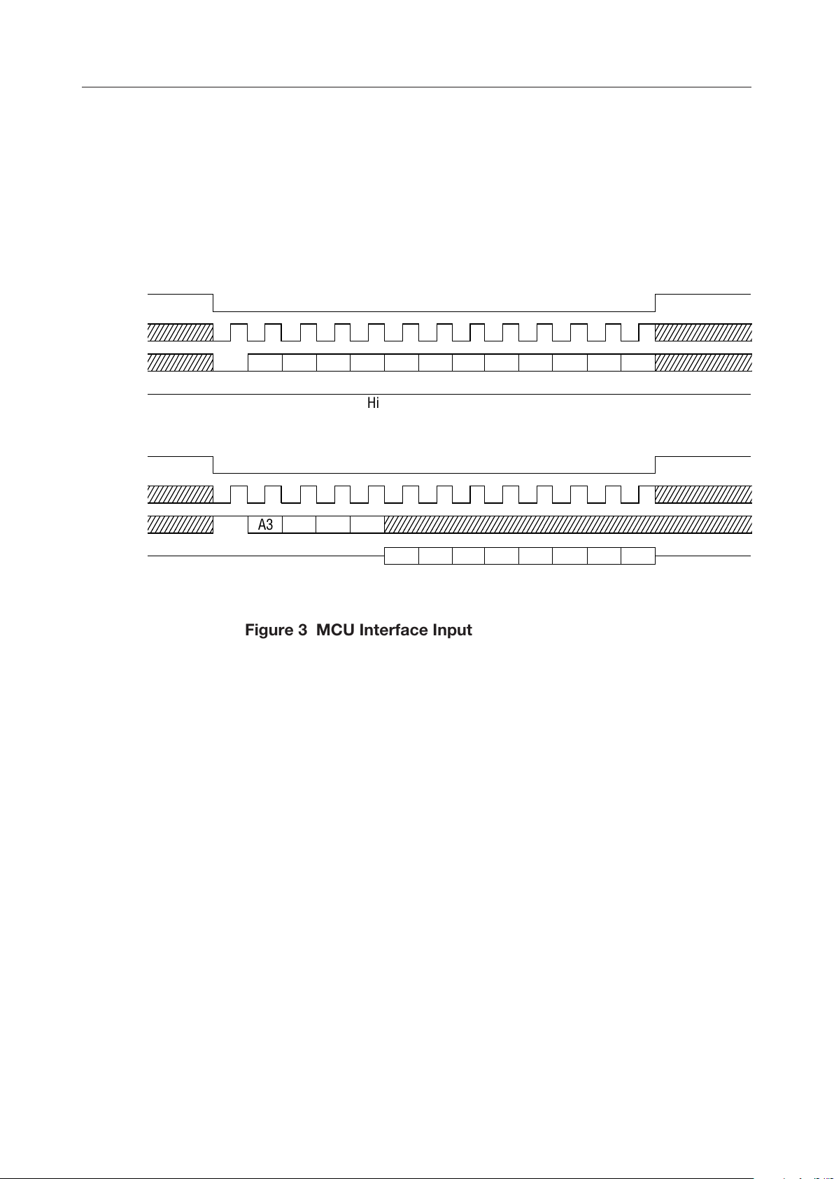
DEN, EXCK, DIN, DOUT
Serial control ports for MCU interface.
Reading and writing data is performed by an external CPU through these pins. 14-byte control
registers (CR0 - 13) are provided in this device.
DEN is the "Enable" control signal input, EXCK is the data shift clock input, DIN is the address
and data input, and DOUT is the data output.
Input/output timing is shown in Fig. 3.
DEN
EXCK
DIN
DOUT
DEN
EXCK
DIN
DOUT
W
R A2A1A0
High Impedance
A3
A3
A2
A1 A0 B7 B6 B5 B4 B3 B2 B1 B0
High Impedance
(a) Write Data Timing Diagram
B7 B6 B5 B4 B3 B2 B1 B0
(b) Read Data Timing Diagram
Figure 3 MCU Interface Input/Output Timing
MUTE
This pin is used to enable the receive side voice path mute level.
To set the mute level, set this pin to "1".
MLV0, MLV1, MLV2
This pin is used to set the receive side voice path mute level.
For the control method, refer to the control register description (CR1). Since these signals are
ORed with CR1 - B2, B1, and B0 internally, set these register data to "0" when using this pin.
11/38
Page 12

¡ Semiconductor MSM7708-02
The register map is shown in Table 1.
Table 1 Control Register (CR0 to CR13) Map
Register
Name
CR0 0 0
CR1 0 001
CR2 0 100
CR3 0 101
CR4 0 010
CR5 0 011
CR6 0 110
CR7 0 111
CR8 1 000
CR9 1 001
Address
A2
A3 A1
0
A0
0
GAIN3TXGAIN2
Side Tone
OTHERS SEL
SEND/
ON/OFFONLVL1
B7
A/m
SEL
TX
MUTERXON/OFF
TX
GAIN2
DTMF/
REC
VOX
VOX
OUT
ST0 ST1
ST8 ST9
B6 B5 B4 B3 B2 B1 B0
Spprs
ON
Side Tone
GAIN1
TONE
SEND
ROW/
SR
SILENCE
LVL1
Data Description
PDN
ALL
ADPCM
RESETTXON/OFFRXMUTERXMLV2RXMLV1RXMLV0
TX
GAIN1TXGAIN0RXGAIN3RXGAIN2RXGAIN1RXGAIN0
Side Tone
GAIN0
TONE5
4M8M/
1M
ON
LVL0
SILENCE
LVL0
ST2 ST3 ST4 ST5 ST6 ST7
ST10 ST11 ST12 — — —
PDN
TX
TONE
ON/OFF
TONE4 TONE3 TONE2 TONE1 TONE0
—
OFF
TIME
— — — BUSY RPM
PDNRXSA,VF
OUT
TONE
GAIN3
— — CMD1 CMD0
VOX
IN
TONE
GAIN2
RX NOISE
LEVEL SEL
SAO/
VFRO
TONE
GAIN1
RX NOISE
LVL1
GAIN0
RX NOISE
AOUT
PON
TONE
LVL0
R/W
R/W
R/W
R/W
R/W
R/W
R/W
R/W
R
R/W
R/W
CR10 1 100
CR11 1 101
CR12 1 010
CR13 1 011
SPY0 SPY1
SP0 SP1
SP8 SP9
CH0 CH1
SPY2 SPY3 SPY4 SPY5 SPY6 SPY7
SP2 SP3 SP4 SP5 SP6 SP7
SP10 SP11 SP12 — — —
CH2 CH3 CH4 — ADRD ADWT
Note : Details are explained in the Control Register Description.
R/W: Both read and write are supported R: Read-only register
R/W
R/W
R/W
R/W
12/38
Page 13

¡ Semiconductor MSM7708-02
(Register Controllers)
DIO
This I/O pin is used to output the write data and fetch the read data.
Connect this pin to the DIN and DOUT pins of the serial register and to the DOUT pin of the serial
voice ROM.
WE
This output pin is used to select the read or write mode.
Connect this pin to the WE pin of the serial register.
SAD
This pin is used to output the read/write start address data.
Connect this pin to the SAD pin of the serial register and to the SADX pin of the serial voice ROM.
SAS
This clock output pin is used to write the serial address.
Connect this pin to the SAS pin of the serial register and to the SASX and SASY pins of the serial
voice ROM.
TAS
This output pin is used to set the serial address input from the SAD pin into the address counter
inside the serial register/serial voice ROM.
Connect this pin to the TAS pin of the serial register/serial voice ROM.
RWCK
This clock output pin is used to write or read data to or from the serial register.
Connect this pin to the RWCK pin of the serial register and to the RDCK pin of the serial voice
ROM.
CS1, CS2
CS1 and CS2 are chip select pins.
Connect CS1 to the CS pin of the serial register, and CS2 to the CS pin of the serial voice ROM.
13/38
Page 14

¡ Semiconductor MSM7708-02
ABSOLUTE MAXIMUM RATINGS
Parameter
Power Supply Voltage
Analog Input Voltage
Digital Input Voltage
Operating Temperature
Storage Temperature
Symbol
V
DD
V
AIN
V
DIN
T
op
T
STG
Condition
—
—
—
—
—
RECOMMENDED OPERATING CONDITIONS
Parameter
Power Supply Voltage
High Level Input Voltage
Low Level Input Voltage
Digital Input Rise Time
Digital Input Fall Time
Digital Output Load
Bypass Capacitor for SG
Master Clock Frequency
Master Clock Duty Ratio
Bit Clock Frequency
Synchronous Signal Frequency
Clock Duty Ratio
Transmit Sync Pulse Setting Time
Receive Sync Pulse Setting Time
Synchronous Signal Width
PCM, ADPCM Setup Time
PCM, ADPCM Hold Time
Symbol
V
DD
V
IH
V
IL
t
Ir
t
If
R
DL
C
DL
C
SGT
C
SGR
F
MCK
D
MCK
F
BCK
F
SYNC
D
CK
t
XS, tSX
t
RS, tSR
t
WS
t
DS
t
DH
Condition
Voltage must be fixed
To all digital input pins
To all digital input pins
To all digital input pins
To all digital input pins
IS (Pull-up resistor)
To all digital output pins
Between SGT and AG
Between SGR and AG
MCK
MCK
BCLK
XSYNC, RSYNC
BCLK, EXCK
BCLK´XSYNC
BCLK´RSYNC
XSYNC, RSYNC
—
—
(V
Fig.4
Rating
–0.3 to +5
–0.3 to V
–0.3 to V
DD
DD
+ 0.3
+ 0.3
–25 to +70
–55 to +150
= 2.7 V to 3.6 V, Ta = –25°C to +70°C)
DD
Min.
2.7
Typ.
—
Max.
3.6
0.45 ¥
V
DD
—
V
DD
0.16 ¥
0
—
—
500
—
10 + 0.1
1
–0.01%
40
64
—
40
100
100
1 BCLK
100
100
—
—
—
—
—
—
—
19.2
50
—
8.0
50
—
—
—
—
—
V
DD
50
50
—
100
—
—
0.01%
60
2048
—
60
—
—
100
—
—
Unit
V
V
V
°C
°C
Unit
V
V
V
ns
ns
W
pF
mF
mF
MHz
%
kHz
kHz
%
ns
ns
ms
ns
ns
14/38
Page 15

¡ Semiconductor MSM7708-02
ELECTRICAL CHARACTERISTICS
DC Characteristics
=
(V
2.7 V to 3.6 V, Ta = –25°C to +70°C)
DD
Parameter
Power Supply Current
Input Leakage Current
High Level Output Voltage
Low Level Output Voltage
Output Leakage Current
Input Capacitance
Symbol
I
DD1
I
DD2
I
IH
I
IL
V
OH1
V
OH2
V
OL
I
O
C
IN
Condition
Min.
Typ.
Max.
Unit
When operating
(When no signal, and VDD = 3.0 V)
— 6.0 11.0 mA
When powered down
(When V
=
V
I
=
V
I
=
I
OH
=
I
OH
I
= –1.2 mA
OL
= 3.0 V)
DD
V
DD
0 V
0.4 mA
1 mA—V
(IS pin is pulled up with
— 0.02 0.1 mA
—
—
0.5 ¥ V
0.8 ¥ V
0
DD
DD
—
—
—
0.2
2.0
0.5
V
0.4
DD
DD
mA
mA
V
V
V
500 W resistor)
IS pin
—
—
10
mA
— —5—pF
15/38
Page 16

¡ Semiconductor MSM7708-02
Analog Interface Characteristics
(V
= 2.7 V to 3.6 V, Ta = –25°C to +70°C)
DD
Parameter
Symbol
Condition
Min.
Typ.
Max.
Unit
Input Resistance
Output Resistance Load
Output Capacitance Load
AIN+, AIN–, AIN2, PWI
R
IN
R
GSX1, GSX2, VFRO, SAO
L1
R
AOUT+, AOUT–
L2
GSX1, GSX2, VFRO, SAO
C
L1
C
AOUT+, AOUT–
L2
GSX1, GSX2, VFRO,
V
Output Voltage Level (*1)
Offset Voltage
SGT, SGR Output Voltage V
SGT Output Impedance R
SGR Output Impedance R
V
V
V
O1
O2
OF1
OF2
SG
SGT
SGR
SAO(R
AOUT+, AOUT–
(RL = 1.2 kW)
VFRO, SAO
= 20 kW)
L
*1 –7.7 dBm (600 W) = 0 dBm0, +3.14 dBm0 = 1.30 VPP.
Digital Interface Characteristics
Parameter
Digital Output Delay Time
PCM, ADPCM Interface
Serial Port Digital I/O
Timing Characteristics
EXCK Clock Frequency F
Symbol
t
SDX, tSDR
t
XD1, tRD1
t
XD2, tRD2
t
XD3, tRD3
t
1
t
2
t
3
t
4
t
5
t
6
t
7
t
8
t
9
t
10
t
11
t
12
EXCK
Condition
1 LSTTL + 100 pF
pull-up resistor : 500 W
Items in parenthesis
mean C load = 10 pF, and
the pull-up resistor £ 2 kW
C load = 50 pF Fig. 5
EXCK — — — 10 MHz
–100
(V
= 2.7 V to 3.6 V, Ta = –25°C to +70°C)
DD
Reference
Fig. 4
10
20
—
—
—
—
MW
kW
1.2 — — kW
—
—
100
pF
— — 100 pF
—
—
1.3
— — 1.3 V
—
+100
V
PP
PP
mV
–20 — +20 mVGSX1, GSX2, AOUT+, AOUT–
— 1.4 — VSGT, SGR
—4080kWSGT
—812kWSGR
Min.
0
0— ns
0— ns
0— ns
Typ.
—
Max.
200 (100)
200 (100)
200 (100)
200 (100)
Unit
ns
50 — — ns
50 — — ns
50 — — ns
50 — — ns
100 — — ns
50 — — ns
50 — — ns
0 — 100 ns
50 — — ns
50 — — ns
0 — 50 ns
200 — — ns
16/38
Page 17

¡ Semiconductor MSM7708-02
Serial Register Interface Characteristics
Parameter
Control Register Data Input
Busy Bit
RPM Bit
Symbol
t
CRW
t
CRR
t
BSR
t
BSH
t
RPR
t
RPF
Condition
Write
Reset
Setup time
Valid time
Setup time
Hold time after
stop command
= 2.7 V to 3.6 V, Ta = –25˚C to +70˚C)
(V
DD
Reference
Fig. 6
Min.
—
—— ns
Typ.
—
Max.
200
200
Unit
ns
——10ms
—— ms
450
——15ms
—— ms
140
17/38
Page 18

¡ Semiconductor MSM7708-02
AC Characteristics
= 2.7 V to 3.6 V, Ta = –25°C to +70°C)
(V
DD
Parameter
Transmit Frequency
Response
Receive Frequency
Response
Transmit Signal to
Distortion Ratio (*1)
Receive Signal to
Distortion Ratio (*1)
Transmit Gain
Tracking
Receive Gain
Tracking
Symbol
Frequency (Hz)
L
L
L
L
L
L
L
L
L
L
L
OSS
OSS
OSS
OSS
OSS
OSS
OSS
OSS
OSS
OSS
OSS
T1
T2
T3
T4
T5
T6
R1
R2
R3
R4
R5
0 to 60
300 to 3000
1020
3300
3400
3968.75
0 to 3000
1020
3300
3400
3968.75
SD T1 35 —
SD T2 35 —
SD T3 35 —
1020
SD T4 28 —
SD T5 23 —
SD R1 —
SD R2 —
SD R3 —
1020
SD R4 —
SD R5 —
GT T1 –0.2 +0.2
GT T2 Reference
GT T3 –0.2 +0.2
1020
GT T4 –0.5 +0.5
GT T5 –1.2 +1.2
GT R1 –0.2 +0.2
GT R2 Reference
GT R3
1020 –0.2 +0.2
GT R4 –0.5 +0.5
GT R5 –1.2 +1.2
Condition
Level dBm0
0
0
3
0
–30
–40
–45
3
0
–30
–40
–45
3
–10
–40
–50
–55
3
–10
–40
–50
–55
Min.
25
Typ.
—
Max.—Unit
dB
–0.15 — +0.20 dB
Reference dB
–0.15 — +0.80 dB
0 — 0.80 dB
13——dB
–0.15 — +0.20 dB
Reference dB
–0.15 — +0.80 dB
0 — 0.80 dB
13——dB
dB
dB
dB
dB
dB
dB
dB
dB
dB
dB
dB
35
35
35
28
23
—
—
—
—
—
—
—
—
—
—
—
dB
—
—
—
—
dB
dB
dB
dB
dB
—
—
—
dB
dB
dB
*1 P-message filter used
18/38
Page 19

¡ Semiconductor MSM7708-02
AC Characteristics (Continued)
= 2.7 V to 3.6 V, Ta = –25°C to +70°C)
(V
DD
Parameter
Symbol
Frequency (Hz) Other
Condition
Min. Typ. Max. Unit
Level dBm0
–68
Idle Channel Noise
(*1)
Absolute Level (*3)
Rejection Ratio
N
IDLT
N
IDLR
A
A
P
SRRT
P
SRRR
VT
VR
———
AIN = SG
—
(–75.7)
–72
——
(*2)
—
—
(–79.7)
1020
Noise frequency:
0
GSX2
VFRO
Noise level:
0.285 0.320 0.359
0.285 0.320 0.359
30——dBPower Supply Noise
—
0 to 50 kHz
50 mVpp
30——dB
*1 P-message filter used
*2 PCMRI input: "11010101" (A-law), "11111111" (m-law)
*3 0.320 Vrms = 0 dBm0 = –7.7 dBm (600 W)
ADPCM unit characteristics are fully compliant with ITU-T Recommendation G.721.
AC Characteristics (DTMF and Other Tones)
= 2.7 V to 3.6 V, Ta = –25°C to +70°C)
(V
DD
Parameter
Symbol
D
Frequency Deviation
D
V
Tone Reference
V
Output Level
V
(*1)
V
DTMF Tone Level Relative Value
R
DTMFVTH/VTL
DTMF tones, Other various tones –1.5 — +1.5 %
FT1
Tone scale
FT2
Transmit side tone
TL
(Gain setting 0 dB)
TH
Receive side tone
RL
(Gain setting –6 dB)
RH
, VRH/V
Condition
DTMF (low group)
DTMF (high group), other
DTMF (low group)
DTMF (high group), other
RL
Min. Typ. Max. Unit
–1.0 — +1.0 %
–18
–16
–10
–8
1dB
–16
–14
–8
–6
2
–14
–12
–6
–4
3
dBmOp
(dBmp)
Vrms
Vrms
dBm0
dBm0
dBm0
dBm0
*1. Not including programmable gain set values
AC Characteristics (Gain Settings)
Parameter
Transmit/Receive Gain
Setting Accuracy
Symbol
D
G
For all gain set values –1 0 +1 dB
Condition
AC Characteristics (Voice/Silence Detect Function)
Parameter
Transmit Voice/Silence
Detection Time
Transmit Voice
Detection Level Accuracy
Symbol
T
VXON
T
VXOF
D
VX
SilenceÆvoice
VoiceÆsilence
For detection level set values by
CRM6 - B6, B5
Condition
VOXO pin: See Fig. 2
Voice/silence
differential: 10 dB
= 2.7 V to 3.6 V, Ta = –25°C to +70°C)
(V
DD
Min. Typ. Max. Unit
= 2.7 V to 3.6 V, Ta = –25°C to +70°C)
(V
DD
Min. Typ. Max. Unit
—5—ms
140/300 160/320 180/340 ms
–2.5 dB
0 2.5
19/38
Page 20

¡ Semiconductor MSM7708-02
TIMING DIAGRAM
Transmit Side PCM, ADPCM Timing
BCLK
XSYNC
PCMSO
BCLK
0
t
XS
t
SDX
t
XS
12345678910
t
SX
t
XD1
t
t
WS
XD2
MSB LSB
123456789100
t
SX
XSYNC
IS
t
SDX
t
XD1
t
XD2
MSB LSB
Receive Side PCM, ADPCM Timing
BCLK
RSYNC
IR
0 10
t
RS
123456789
t
SR
t
WS
t
t
DH
DS
MSB
t
XD3
LSB
t
t
XD3
XD3
BCLK
t
RS
123456789100
t
SR
RSYNC
t
RD2
MSB LSB
PCMRO
t
SDX
t
RD1
Figure 4 PCM, ADPCM Interface
Serial Port Timing for Microcontroller Interface
DEN
t
2
EXCK
DIN
t
1
123456
t
3
t
4
t
6
W/R A3 A2 A1 A0
t
RD3
t
t
5
12
t
10
11 12
t
7
B7
t
8
t
9
B1 B0
t
11
DOUT
B7
Figure 5 Serial Control Port Interface
B1 B0
20/38
Page 21

¡ Semiconductor MSM7708-02
Address Write/Read Mode Timing
DEN
EXCK
DIN
XX
(CR13)
(ADWT, ADRD)
CR13-(B1, B0)
BUSY
Serial Register
I/F
Record/Playback Mode Timing
DEN
EXCK
t
CRW
t
BSR
(X, X) (0, 0)
Address Data Transfer
t
BSH
t
CRR
DIN
(CR5)
CR5-(B1, B0)
RPM
Serial Register
I/F
XX
(PLAY/REC)
"1" "1"
(X, X) (0, 0)
t
CRW
t
RPR
Record/Playback Data Transfer
Figure 6 Serial Register Interface
(STOP)
t
RPF
t
CRR
21/38
Page 22

¡ Semiconductor MSM7708-02
FUNCTIONAL DESCRIPTION
Control Register Description
(1) CR0 (Basic Operation Mode Settings)
CR0
Initial value
B7
A/m
SEL
0
B6
—
0
B5
PDN
ALL
0
B4
PDN
TX
0
B3
PDN
RX
0
B2
SA, VF
OUT
0
B1
SAO/
VFRO
0
B0
AOUT
PON
B7: ..............PCM interface companding law selection 0: m-law1: A-law
B6: ..............Automatic suppression function control 0: suppression off
1: suppression on
When transmit voice is detected, receive level is suppressed automatically
by 6 dB.
B5: ..............Power down (entire unit) 0: Power ON 1: Power down
ORed with the inverted external power down signal. When using this
data, set PDN to "1".
B4: ..............Power down (transmit side only) 0: Power ON 1: Power down
B3: ..............Power down (receive side only) 0: Power ON 1: Power down
B2: ..............The sounder output amp (SAO) and receiver system output amp
(VFRO) operation control
0: The output pin selected by CR0 - B1 operates.
1: The sounder system output (SAO) and receiver system output (VFRO)
both operate.
B1: ..............Selection of sounder system output (SAO) or receiver system output
0: VFRO 1: SAO
SGR potential is output to the non selected pin.
B0: ..............AOUT+, AOUT– power on control
0: AOUT+, – power down
1: AOUT+, – power on
0
22/38
Page 23

¡ Semiconductor MSM7708-02
(2) CR1 (ADPCM Operation Mode Settings)
CR1
Initial value
B7
TX
MUTE
0
B6
RX
ON/OFF
0
B5
ADPCM
RESET
0
B4
TX
ON/OFF
0
B3
RX
MUTE
0
B2
RX
MLV2
0
B1
RX
MLV1
0
B0
RX
MLV0
0
B7: ..............Transmit side ADPCM data MUTE 1: MUTE
B6: ..............Receive side PCM signal ON/OFF 0: ON 1: OFF
B5: ..............Transmit/Receive side ADPCM RESET (in accordance with the G.721)
1: RESET
B4: ..............Transmit side PCM signal ON/OFF 0: ON 1: OFF
PCM idle pattern is transmitted when set OFF
B3: ..............Receive side ADPCM data MUTE 1: MUTE
Mute operation set by B2, 1, 0 is available, provided this
bit is valid when MUTE pin is "0".
B2, 1, 0: ......Receive side voice path mute level settings
(MLV2, MLV1, MLV0) = (0, 0, 0) : through
(0, 0, 1) : –6 dB
(0, 1, 0) : –12 dB
(0, 1, 1) : –18 dB
(1, 0, 0) : –24 dB
(1, 0, 1) : –30 dB
(1, 1, 0) : –36 dB
(1, 1, 1) : MUTE
Note: The above settings are not applied to various tone, side tone, and background noise.
23/38
Page 24

¡ Semiconductor MSM7708-02
(3) CR2 (PCM CODEC Operation Mode Settings and Transmit/Receive Gain Adjustment)
CR2
Initial value
B7
1
1
1
1
1
1
1
1
0
0
0
0
0
0
0
0
B7
TX
GAIN3
0
B6
TX
GAIN2
0
B5
TX
GAIN1
0
B4
TX
GAIN0
0
B3
RX
GAIN3
0
B2
RX
GAIN2
0
GAIN1
B7, B6, B5, B4: .... Transmit side signal gain adjustment (refer to Table 2)
B3, B2, B1, B0: .... Receive side signal gain adjustment (refer to Table 2)
Table 2 Transmit/Receive Gain Settings
B6
B5
0
1
0
0
1
1
1
1
0
0
0
0
1
1
1
1
B4
Transmit Side Gain
0
0
1
1
0
0
1
1
0
0
1
1
0
0
1
1
0
1
0
1
0
1
0
1
0
1
0
1
0
1
0
1
–16 dB
–14 dB
–12 dB
–10 dB
–8 dB
–6 dB
–4 dB
–2 dB
0 dB
+2 dB
+4 dB
+6 dB
+8 dB
+10 dB
+12 dB
+14 dB
B3
1
1
1
1
1
1
1
1
0
0
0
0
0
0
0
0
B2
0
1
0
0
1
1
1
1
0
0
0
0
1
1
1
1
B1
0
0
1
1
0
0
1
1
0
0
1
1
0
0
1
1
B0
0
1
0
1
0
1
0
1
0
1
0
1
0
1
0
1
Receive Side Gain
B1
RX
0
B0
RX
GAIN0
0
–16 dB
–14 dB
–12 dB
–10 dB
–8 dB
–6 dB
–4 dB
–2 dB
0 dB
+2 dB
+4 dB
+6 dB
+8 dB
+10 dB
+12 dB
+14 dB
The above gain settings table shows the transmit/receive voice signal gain settings and the
transmit side gain settings for DTMF tones and other tones. Tone signal transmission is enabled
by CR4 - B6 (discussed later), and the gain setting is set to the levels shown below.
DTMF tones (low group): ................................. –16 dBm0
DTMF tones (high group) and other tones: ... –14 dBm0
For example, if the transmit gain set value is set to +8 dB (B7, B6, B5, B4) = (0, 1, 0, 0), then the
following tones appear at the PCMSO pin.
DTMF tones (low group): ................................. –8 dBm0
DTMF tones (high group) and other tones: ... –6 dBm0
However, the gain of the receive side tone and the gain of the side tones (path from transmit side
to receive side) are set by the CR3 register.
24/38
Page 25

¡ Semiconductor MSM7708-02
(4) CR3 (Side Tone and Tone Generator Gain Adjustment)
CR3
Initial value
B7
Side Tone
GAIN2
0
B6
Side Tone
GAIN1
0
B5
Side Tone
GAIN0
0
B4
TONE
ON/OFF
0
B3
TONE
GAIN3
0
B2
TONE
GAIN2
0
B1
TONE
GAIN1
0
B0
TONE
GAIN0
0
B7, B6, B5: ........ Side tone gain adjustment (refer to Table 3)
B4: ..................... Tone generator ON/OFF 0: OFF 1: ON
B3, B2, B1, B0: . Tone generator Receive side gain adjustment (refer to Table 4)
Table 3 Side Tone Gain Settings
B7 B6 B5
0
0
0
0
1
1
1
1
0
0
1
1
0
0
1
1
0
1
0
1
0
1
0
1
Side Tone Gain
OFF
–15 dB
–13 dB
–11 dB
– 9 dB
– 7 dB
– 5 dB
– 3 dB
Table 4 Receive Side Tone Generator Gain Settings
B3
B2
0
0
0
0
0
0
0
0
B1
0
0
0
0
1
1
1
1
B0
Tone Generator Gain
0
0
1
1
0
0
1
1
0
1
0
1
0
1
0
1
–36 dB
–34 dB
–32 dB
–30 dB
–28 dB
–26 dB
–24 dB
–22 dB
B3
1
1
1
1
1
1
1
1
B2
0
0
0
0
1
1
1
1
B1
0
0
1
1
0
0
1
1
B0
Tone Generator Gain
0
1
0
1
0
1
0
1
–20 dB
–18 dB
–16 dB
–14 dB
–12 dB
–10 dB
– 8 dB
– 6 dB
The receive side tone generator gain settings shown in Table 4 are set with the following levels
as a reference.
DTMF tones (low group): ................................. –2 dBm0
DTMF tones (high group) and other tones: ... 0 dBm0
For example, if the tone generator gain set value is set to –6 dB (B3, B2, B1, B0)=(1, 1, 1, 1), then
tones at the following levels appear at the SAO or VFRO pin.
DTMF tones (low group): ................................. –8 dBm0
DTMF tones (high group) and other tones: ... –6 dBm0
25/38
Page 26

¡ Semiconductor MSM7708-02
(5) CR4 (Tone Generator Operation Mode and Frequency Settings)
B7
CR4
Initial value
DTMF/
OTHERS SEL
0
TONE
SEND
B7: ........................... Selection of DTMF signal and other tones
(S tone, F tone, R tone, etc.) 0: Other tones 1: DTMF tones
B6: ........................... Transmission side tone transmit
0: Voice signal transmit 1: Tone transmit
B5, B4, B3, B2, B1, B0: .. Tone frequency setting (refer to Table 5)
Table 5 DTMF Signal and Other Tone Settings
(a) When B7 = 1 (DTMF Tones)
B5 B4 B3 B2 B1 B0
**0000
**0001
**0010
**0011
**0100
**0101
**0110
**0111
697 Hz + 1209 Hz
697 Hz + 1336 Hz
697 Hz + 1477 Hz
697 Hz + 1633 Hz
770 Hz + 1209 Hz
770 Hz + 1336 Hz
770 Hz + 1477 Hz
770 Hz + 1633 Hz
B6
TONE5
0
Description
B5
0
B4
TONE4
0
B5 B4 B3 B2 B1 B0
**1000
**1001
**1010
**1011
**1100
**1101
**1110
**1111
B3
TONE3
0
B2
TONE2
0
B1
TONE1
0
Description
852 Hz + 1209 Hz
852 Hz + 1336 Hz
852 Hz + 1477 Hz
852 Hz + 1633 Hz
941 Hz + 1209 Hz
941 Hz + 1336 Hz
941 Hz + 1477 Hz
941 Hz + 1633 Hz
B0
TONE0
0
26/38
Page 27

¡ Semiconductor MSM7708-02
(b) When B7 = 0 (Other than DTMF Tones)
B5 B4 B3 B2 B1 B0
000000
000001
000010
000011
000100
000101
000110
000111
001000
001001
001010
001011
001100
001101
001110
001111
010000
010001
010010
010011
010100
010101
010110
010111
011000
011001
011010
011011
011101
011101
011110
011111
Description
784.0 Hz (G)
830.6 Hz (G+)
880.0 Hz (A)
932.3 Hz (A+)
987.8 Hz (B)
1046.5 Hz (C)
1108.7 Hz (C+)
1174.7 Hz (D)
1244.5 Hz (D+)
1318.5 Hz (E)
1396.9 Hz (F)
1480.0 Hz (F+)
1568.0 Hz (G)
1661.2 Hz (G+)
Tone Scale
1760.0 Hz (A)
1864.7 Hz (A+)
1975.5 Hz (B)
2093.0 Hz (C)
2217.5 Hz (C+)
2349.3 Hz (D)
2489.0 Hz (D+)
2637.0 Hz (E)
2793.8 Hz (F)
2960.0 Hz (F+)
3136.0 Hz (G)
400 Hz
500 Hz
600 Hz
700 Hz
800 Hz
900 Hz
1000 Hz
B5 B4 B3 B2 B1 B0
100000
100001
100010
100011
100100
100101
100110
100111
101000
101001
101010
101011
101100
101101
101110
101111
110000
110001
110010
110011
110100
110101
110110
110111
111000
111001
111010
111011
111100
111101
111110
111111
Description
1100 Hz
1200 Hz
1300 Hz
1400 Hz
1500 Hz
1600 Hz
1700 Hz
1800 Hz
1900 Hz
2000 Hz
2100 Hz
2200 Hz
2300 Hz
2400 Hz
2500 Hz
2600 Hz
2700 Hz
2800 Hz
2900 Hz
3000 Hz
2760 Hz
—
—
—
—
—
—
—
—
—
—
—
27/38
Page 28

¡ Semiconductor MSM7708-02
(6) CR5 (Serial Register Interface Control)
CR5
Initial value
B7
SEND/
REC
0
B6
ROM/
SR
0
B5
4M8M/
1M
0
B4
—
0
B3
—
0
B2
—
0
B1
CMD1
0
B0
CMD0
0
B7: ..............Connection between register and ADPCM
0: with ADPCM receive side 1: ADPCM Transmit side
B6: ..............Voice ROM/Serial register selection
0: Serial Register 1: Voice ROM
B5: ..............Connecting serial register capacity
0: 1 Mb (MSM63V89C)
1: 4 Mb (MSM6684), 8 Mb (MSM6685)
B4 - B2: ......Reserved for test. Should be set "0"
B1, B0: ....... Serial register I/F Instruction command
(CMD1, CMD0) = (0, 0) : NOP
(0, 1) : PLAY (Playback)
(1, 0) : REC (Recording)
(1, 1) : STOP (Stop)
* (CMD1, CMD0) are reset (0, 0) after command execution.
Instruction commands of Play and REC should not be set when busy (CR5 - B1) and
RPM (CR5 - B0) are "1".
(7) CR6 (VOICE/SILENCE Detect Function Control)
CR6
Initial value
B7
VOX
ON/OFF
0
B6
ON
LVL1
0
B5
ON
LVL0
0
B4
OFF
TIME
0
B7: ..............Voice/Silence detect function ON/OFF 0: OFF 1: ON
B6, B5: ....... Transmit side voice/silence detector level settings
(0,0): –20 dBm0 (0,1): –25 dBm0
(1,0): –30 dBm0 (1,1): –35 dBm0
B4: ..............Hangover time (refer to Fig. 1) settings 0: 160 ms 1: 320 ms
B3: ..............Receive side Voice/Silence detect input signal
0: Internal background noise transmit 1: Voice receive signal transmit
When using this data, set the VOXI pin to "0".
B2: ..............Receive side background noise level setting
0: Internal automatic setting 1: External (by B1, B0) setting
Internal automatic setting Æ Set to the voice signal level when B3 (VOXI)
changes from "1" to "0".
B1, B0: ....... External setting background noise level
(0,0): No noise (0,1): –55 dBm0
(1,0): –45 dBm0 (1,1): –35 dBm0
B3
VOX
IN
0
B2
RX NOISE
LEVEL SEL
0
B1
RX NOISE
LVL1
0
B0
RX NOISE
LVL0
0
28/38
Page 29

¡ Semiconductor MSM7708-02
(8) CR7 (Detect Register: Read-only)
CR7
Initial value
B7
VOX
OUT
0
B6
Silent Level
1
0
B5
Silent Level
0
0
B4
—
0
B3
—
0
B2
—
0
B1
Busy
0
B0
RPM
0
B7: ..............Transmit side voice/silence detection 0: Silence 1: Voice
B6, B5: ....... Transmit side silence level (indicator)
(0,0):Below –60 dBm0 (0,1): –50 to –60 dBm0
(1,0): –40 to –50 dBm0 (1,1): Above –40 dBm0
Note: These outputs are enabled when the voice/silence detect function is turned on by CR6
- B7.
B4, B3, B2: .Not used
B1: ..............Serial Register I/F monitoring
Monitors address read and write operation of serial register interface.
0: Stop 1: Read or Write
B0: ..............Monitors serial register recording or playback.
0: Stop 1: Recording or playing back
29/38
Page 30

¡ Semiconductor MSM7708-02
(9) CR8 (Start X address 0-7)
B7
CR8
Initial value
ST0
0
CR9 (Start X address 8-12)
B7
CR9
Initial value
ST8
0
CR8 (B7 - B0), CR9 (B7 - B3): Record and Playback start address store register
(10) CR10 (Stop Y address 0-7)
B7
CR10
Initial value
SPY0
0
SPY1
B6
ST1
0
B6
ST9
0
B6
0
B5
ST2
0
B5
ST10
0
B5
SPY2
0
B4
ST3
0
B4
ST11
0
B4
SPY3
0
B3
ST4
0
B3
ST12
0
B3
SPY4
0
B2
ST5
0
B2
—
0
B2
SPY5
0
B1
ST6
0
B1
—
0
B1
SPY6
0
B0
ST7
0
B0
—
0
B0
SPY7
0
CR10 (B7 - B0): Record and Playback stop Y address store register
(11) CR11 (Stop X address 0-7)
CR11
Initial value
B7
SP0
0
B6
SP1
0
B5
SP2
0
B4
SP3
0
B3
SP4
0
B2
SP5
0
B1
SP6
0
B0
SP7
0
CR12 (Stop X address 8-12)
CR12
Initial value
B7
SP8
0
B6
SP9
0
B5
SP10
0
B4
SP11
0
B3
SP12
0
B2
—
0
B1
—
0
B0
—
0
CR11 (B7 - B0), CR12 (B7 - B3): Record and Playback stop X address store register
Note: The data in CR8 - CR12 may be changed under the following conditions. If so,
rewrite the data.
(1) When REC or Play command is executed during the state of start address = stop
address
(2) When stop command is executed during the state of no operation of serial
register interface (Busy = RPM = "0")
30/38
Page 31

¡ Semiconductor MSM7708-02
(12) CR13 (Channel Selection)
CR13
Initial value
B7
CH0
0
B6
CH1
0
B5
CH2
0
B4
CH3
0
B3
CH4
0
B2
—
0
B1
ADRD
0
B0
ADWT
0
B7 - B3 .......Channel selection (All 32 channels are selected with Hex cord)
B2 ...............Since reserved for TEST, this bit should always be set to "0".
B1 ...............Address read instruction
0: NOP
1: When set to "1", start/stop address corresponding to the channels
specified by B7 to B3 is transferred from serial register channel index area
to CR8 - CR12. After transfer, this bit is reset to "0".
B0 ...............Address write instruction
0: NOP
1: When set to "1", start/stop address corresponding to the channels
specified by B7 to B3 is transferred from CR8 - CR12 to serial register
channel index area. After transfer, this bit is reset to "0".
Note : Writing to ADRD and ADWT is inhibited when BUSY (CR7 - B1) or RPM (CR7 - B0) is
"1".
31/38
Page 32

¡ Semiconductor MSM7708-02
DATA CONFIGURATION IN THE EXTERNAL SERIAL REGISTER
X Address Space
The address space of the external serial register is accessed based on (word direction indicated
by the X address) ¥ (1 Kb depth in Y direction). The maximum X address in word direction
depends on the total memory of serial registers connected. Since the leading 32 words (32 Kb)
of the serial register are used as the channel index area, X address 020h onward can be used as
the voice data area.
CR5-B5 011
Total Memory Capacity
(device name)
Number of words 1K words 4K words 8K words
X address*
* 0000h to 001Fh is used as the channel index area.
1 Mb
(MSM63V89C)
000h to 3FFh 0000h to 0FFFh 0000h to 1FFFh
4 Mb
(MSM6684)
8 Mb
(MSM6685)
Y Address Space
For 1 Kb ADPCM data in Y direction, 4 bits ¥ 256 samples = 1024 bits are stored in the 1 Kb
memory area. One Y address is allocated to one sample (4 bits) of ADPCM data and addressing
is made with 00h to FFh.
X address (1 K words of 000h to 3FFh : 1 word = 1 Kb)
000h
channel index area (32 words ¥ 1 Kb + 32 Kb)
01Fh
020h
1Mb serial register
ADPCM (voice) data area
1 Kb in Y direction
1 word = 1 Kb
Y address
00h 01h FEh FFh
4 bit 4 bit 4 bit 4 bit
3FFh
Figure 7 Address Space of the 1 Mb Serial Register
32/38
Page 33

¡ Semiconductor MSM7708-02
Channel Index Area of the Serial Register
One channel (1 Kb) of the channel index area consists of the 40 bits of address data.
(1) Stop Y address
The Y address is represented by 8 bits and addressing is made with 00h to FFh.
(2) Start X address, stop X address
The X address is represented by 16 bits (valid 13 bits). If, for example, the serial register is
1Mb, the 1K-word X address space is addressed with 000h to 3FFh.
Address
data
40-bit
16-bit 8-bit 16-bit
Start
X address
Start X address (ST0 to ST12)
Stop Y address (SPY0 to SPY7)
Stop X address (ST0 to SP12)
Stop
Y address
Blank data
Stop
X address
ST0 ST1 ST11 ST12 — — —
SPY0 SPY1 SPY6 SPY7
SP0 SP1 SP11 SP12 — — —
Figure 8 Channel Index Area of the Serial Register
33/38
Page 34

¡ Semiconductor MSM7708-02
METHODS OF RECORDING AND PLAYBACK
Recording Method (See the flow chart in Figure 9.)
(1) • Set up the connection between the serial register/
voice ROM and ADPCM transmit-receive
system. (See Figure 11.) (CR5 - B7)
• Specify the serial register/voice ROM. (CR5 B6)
• Set the external capacity. (CR5 - B5)
• Set the NOP command. (CR5 - B1 = "0", B0 = "0")
(2) • Set the start/stop address. (CR8 to CR12)
(3) • Set the channel. (CR13 - B7 to B3)
• Set the ADWT (address write) instruction. (CR13
- B1 = "0", B0 = "1")
(4) • The start/stop address of the channel set by the
ADWT instruction is stored in the channel index
area. When status register BUSY (CR7 - B1)
changes from "1" to "0", storage is complete.
(5) • Start recording by setting the REC (recording)
command (CR5 - B1 = "1", B0 = "0"). In this case,
the basic setting of CR5 - B7 to B5 should be the
same as (1).
(6) • Check the recording start with the status register
RPM bit (CR7 - B0 = "1").
(7) • To interrupt during recording, set the STOP
(stop) command (CR5 - B1 = "1", B0 = "1").
In this case, to store the address counter contents
in the channel index area as a new stop address,
the following settings are required:
• Set the channel.
• Set the ADWT instruction.
• When the BUSY bit changes from "1"
N
to "0", settings are complete.
(8) • When the address counter reaches the
stop address, recording is complete.
Check completion of recording with
RPM bit = "0".
N
N
N
STOP
RPM = 0?
Y
Channel setting
(ADWT)
Recording
BUSY = 0?
RPM = 0?
Y
Basic setting
ST, SP
address setting
Channel setting
(ADWT)
BUSY = 0?
Y
REC
RPM = 1?
Y
(1) CR5
(2) CR8 to CR12
(3) CR13
(4) CR7
(5) CR5
Recording start
(6) CR7
Recording start
check
(7) CR5
Recording stop
CR13
CR7
Note: If the stop address value is smaller
than the start address value,
recording is made to the last address
of the serial register.
N
BUSY = 0?
Y
N
RPM = 0?
Y
END
Figure 9 Flow Chart of Recording
(8) CR7
Recording
completion
check
34/38
Page 35

¡ Semiconductor MSM7708-02
Playback Method (See the flow chart in Figure 10.)
(1) • Set up the connection between
the serial register/voice ROM
and ADPCM transmit-receive
Playback
system. (See Figure 11.) (CR5 B7)
• Specify the serial register/voice
N
BUSY = 0?
RPM = 0?
ROM. (CR5 - B6)
• Set the external capacity. (CR5 B5)
• Set the NOP command. (CR5 B1 = "0", B0 = "0")
(2) • Set the channel. (CR13 - B7 to
Basic setting
Voice ROM
Channel setting
Y
(ADRD)
(1) CR5
(2) CR13
B3)
• Set the ADRD (address read)
instruction. (CR13 - B1 = "1", B0
= "0")
ST, SP
address setting
(3) CR8 to 12
(3) • For playback of the voice ROM,
set the start/stop address here.
N
BUSY = 0?
(4) CR7
(4) • The start/stop address of the
PLAY
Y
(5) CR5
Playback start
channel set by the ADRD
instruction is fetched from the
channel index area.
When status register BUSY (CR7
- B1) changes from "1" to "0",
fetching is complete.
(5) • Start playback by setting the
PLAY (playback) command
N
RPM = 1?
Y
(6) CR7
Playback start
check
(CR5 - B1 = "0", B0 = "1"). In this
case, basic setting of CR5 - B7 to
B5 should be the same as (1).
STOP
(7) CR5
Playback stop
(6) • Check the playback start with
the status register RPM bit (CR7
- B0 = "1").
(7) • To stop playback set the STOP
(stop) command (CR5 - B1 = "1",
B0 = "1").
(8) • When the address counter
reaches the stop address,
N
RPM = 1?
Y
END
(8) CR7
Playback completion
check
playback is complete.
Check completion of playback
Figure 10 Flow Chart of Playback
with RPM bit = "0".
Note: If the stop address value is
smaller than the start address
value, playback is made to the
last address of the serial
register.
35/38
Page 36

¡ Semiconductor MSM7708-02
SIGNAL FLOW IN RECORDING/PLAYBACK
When the serial register is connected to each ADPCM transmit and receive system, the flow of
recording/playback signal is as follows:
Transmit-side recording Transmit-side playback
(CR5 – B7 = "1" + REC) (CR5 – B7 = "1" + PLAY)
IS (ADPCM-OUT)
A-IN
ADPCM
CODER
Serial register
A-IN
ADPCM
CODER
Serial register
Receive-side recording Receive-side playback
(CR5 – B7 = "0" + REC) (CR5 – B7 = "0" + PLAY)
IR (ADPCM-IN)
A-OUT
ADPCM
DE-CODER
A-OUT
ADPCM
DE-CODER
IS (ADPCM-OUT)
IR (ADPCM-IN)
Serial register
Serial register
Figure 11 Signal Flow in Transmit/Receive Side Recording/Playback
36/38
Page 37

¡ Semiconductor MSM7708-02
37/38
APPLICATION CIRCUIT
An application circuit is shown below using a 1 Mb serial register and a 1 Mb serial voice ROM.
Voice analog input (VI)
1 mF 10 mF
1 mF 10 mF
+
–
1 mF
1 mFR1
R2
1 mFR3
R4
R5
R6
Transmit gain (V
GSX2/VI
)
= (R2/R1) ¥ (R4/R3)
Receive gain (V
O/VVFRO
)
= 2 ¥ R6/R5
Receiver output
Sounder output
V
DD
SGT
SGR
AG
DG
AIN1+
AIN1–
GSX1
AIN2
GSX2
VFRO
PWI
AOUT+
SAO
MCK
PDN
RESET
EXCK
DEN
DIN
DOUT
AOUT–
Basic
control
IS
PCMSI
PCMSO
IR
PCMRO
PCMRI
BCLK
XSYNC
YSYNC
VOXO
VOXI
MUTE
MLV3
DIO
MLV1
MLV2
WE
SAD
SAS
TAS
RWCK
CS1
CS2
500 W
ADPCM
transmit data
ADPCM
receive data
ADPCM
control
DIN
DOUT
WE
SAD
SAS
TAS
RWCK
RFSH
FAM
TEST
TEST
RS/A
CS
1 Mb serial register
MSM63V89C
1 Mb serial voice ROM
MSM6595A-XXX
DOUT
SADX
SASX
TAS
RDCK
SASY
SADY
TEST
TEST
CS
MSM7708
Z
L
= 120 nF +
350
W
Page 38

¡ Semiconductor MSM7708-02
PACKAGE DIMENSIONS
(Unit : mm)
TQFP64-P-1010-0.50-K
Mirror finish
Package material
Lead frame material
Pin treatment
Solder plate thickness
Package weight (g)
Epoxy resin
42 alloy
Solder plating
5 mm or more
0.26 TYP.
Notes for Mounting the Surface Mount Type Package
The SOP, QFP, TSOP, SOJ, QFJ (PLCC), SHP and BGA are surface mount type packages, which
are very susceptible to heat in reflow mounting and humidity absorbed in storage.
Therefore, before you perform reflow mounting, contact Oki’s responsible sales person for the
product name, package name, pin number, package code and desired mounting conditions
(reflow method, temperature and times).
38/38
 Loading...