

Page 1

E2U0042-28-81
¡ Semiconductor MSM7705-01/02/03
¡ Semiconductor
This version: Aug. 1998
Previous version: Nov. 1996
MSM7705-01/02/03
4ch Single Rail CODEC
GENERAL DESCRIPTION
The MSM7705-01/02/03 are four-channel CODEC CMOS ICs for voice signals ranging from 300
to 3400 Hz. These devices contain filters for A/D and D/A conversion.
Designed especially for a single-power supply and low-power applications, these devices
contain four-channel A/D and D/A converters in a single chip and achieve a reduced footprint
and a reduced number of external components.
The MSM7705-01/02/03 are best suited for digital telephone terminals, digital PABXs, and pushbutton phones.
FEATURES
• Single power supply: +5 V
• Power consumption
Operating mode: 70 mW Typ. 140 mW Max.
Power-saving mode: 14 mW Typ. 32 mW Max.
Power-down mode: 0.05 mW Typ. 0.3 mW Max.
• Conforms to ITU-T Companding law
MSM7705-01: m/A-law pin-selectable
MSM7705-02: m-law
MSM7705-03: A-law
• Built-in PLL eliminates a master clock
• The PCM interface can be switched between 4 channel serial/parallel
• Transmission clock: 64/128/256/512/1024/2048 kHz
96/192/384/768/1536/1544 kHz
(During 4 channel serial mode, the 64, 96, 128, and 192 kHz clocks are
disabled)
• Transmit gain adjustable for each channel
• Built-in reference voltage supply
• Analog output can directly drive a 600 W line transformer
• Package:
44-pin plastic QFP (QFP44-P-910-0.80-2K) (Product name : MSM7705-01GS-2K)
(Product name : MSM7705-02GS-2K)
(Product name : MSM7705-03GS-2K)
1/20
Page 2
¡ Semiconductor MSM7705-01/02/03
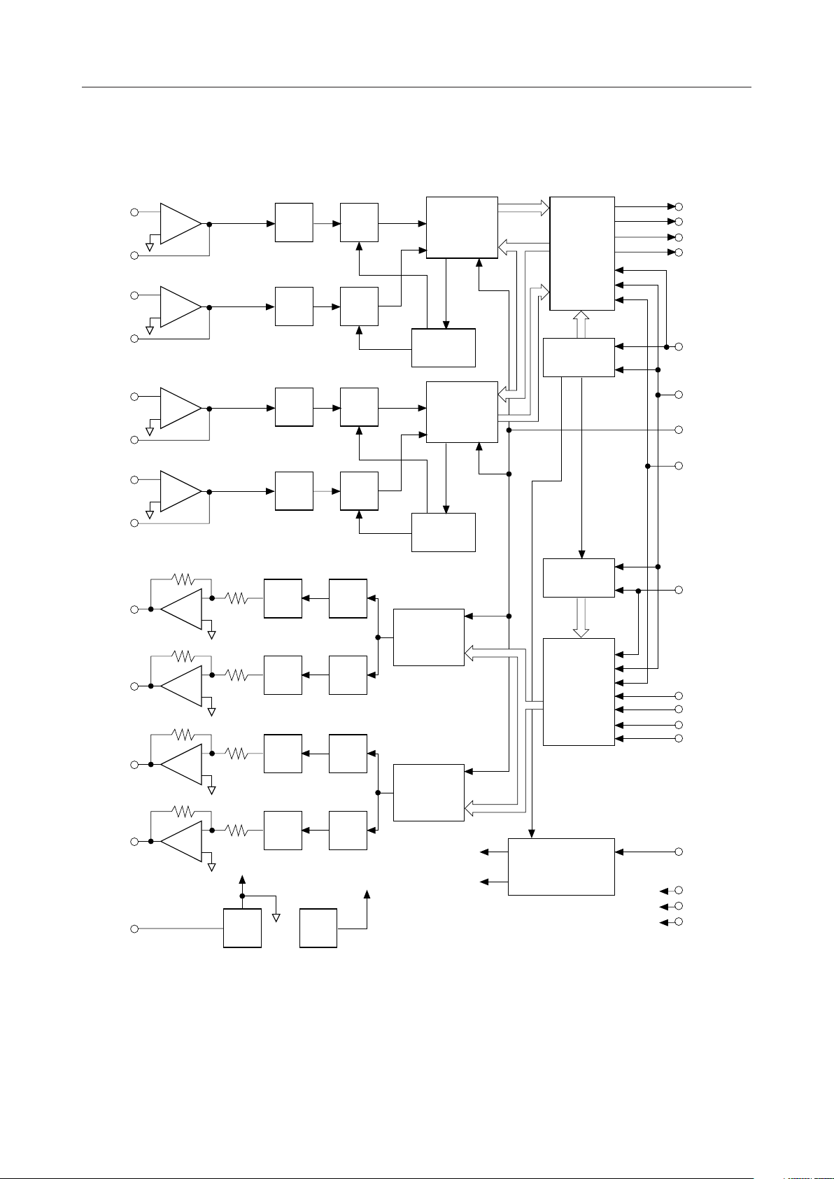
BLOCK DIAGRAM
AIN1
GSX1
AIN2
GSX2
AIN3
GSX3
AIN4
GSX4
AOUT1
AOUT2
AOUT3
AOUT4
SGC
–
+
RC
LPF
8th
BPF
AD
CONV.
TCONT
–
+
RC
LPF
8th
BPF
AUTO
ZERO
–
+
RC
LPF
8th
BPF
AD
CONV.
PLL
DOUT1
DOUT2
DOUT3
DOUT4
XSYNC
BCLK
(ALAW)
CHPS
–
+
RC
LPF
8th
BPF
AUTO
ZERO
RTIM
–
+
5th
LPF
S&H
RSYNC
DA
CONV.
–
+
5th
LPF
S&H
RCONT
DIN1
DIN2
DIN3
–
+
5th
LPF
S&H
DIN4
DA
CONV.
–
+
5th
LPF
S&H
PWD
PDN
Logic
V
DD
AG
SG
GEN
VR
GEN
DG
2/20
Page 3
¡ Semiconductor MSM7705-01/02/03
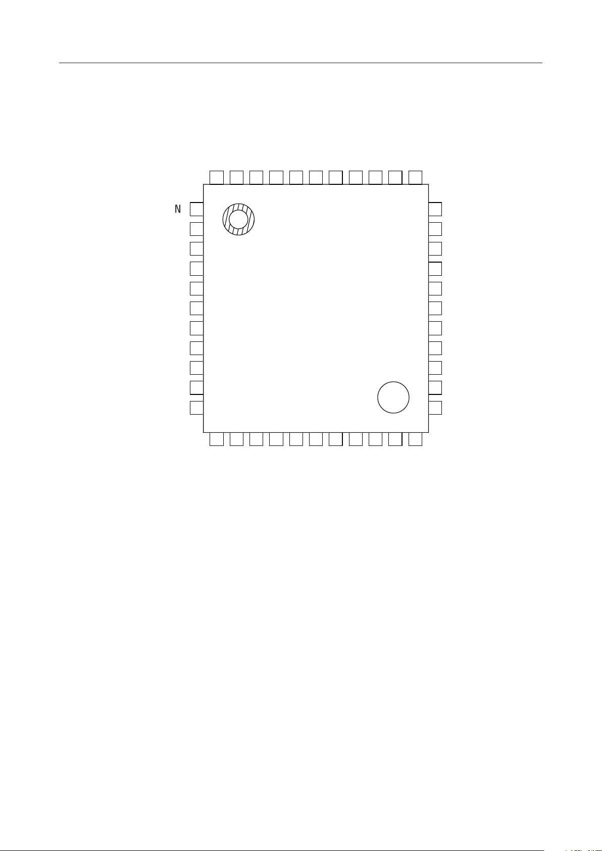
PIN CONFIGURATION (TOP VIEW)
(
AIN3
GSX3
GSX4
AIN4
SGC
AG
AG
AOUT1
AOUT2
AOUT3
AOUT4
44
43
42
41
40
39
38
37
36
35
34
1
NC
2
NC
NC
3
V
4
DD
(
V
DD
NC
NC
5
6
7
33
32
31
30
29
28
27
AIN2
GSX2
GSX1
AIN1
NC
NC
NC
DIN4
DIN3
DIN2
DIN1
10
11
8
9
12
13
14
15
16
17
18
19
20
21
XSYNC
RSYNC
NC
BCLK
NC : No connect pin
44-Pin Plastic QFP
DG
NC
DG
(
DOUT4
DOUT3
DOUT2
26
25
24
23
22
DOUT1
NC
(ALAW)*
PDN
CHPS
VDD, DG, and AG have two pins each. Each of these pairs are internally connected with
each other.
* The ALAW pin is only supported by MSM7705-01GS-2K.
3/20
Page 4
¡ Semiconductor MSM7705-01/02/03
PIN AND FUNCTIONAL DESCRIPTIONS
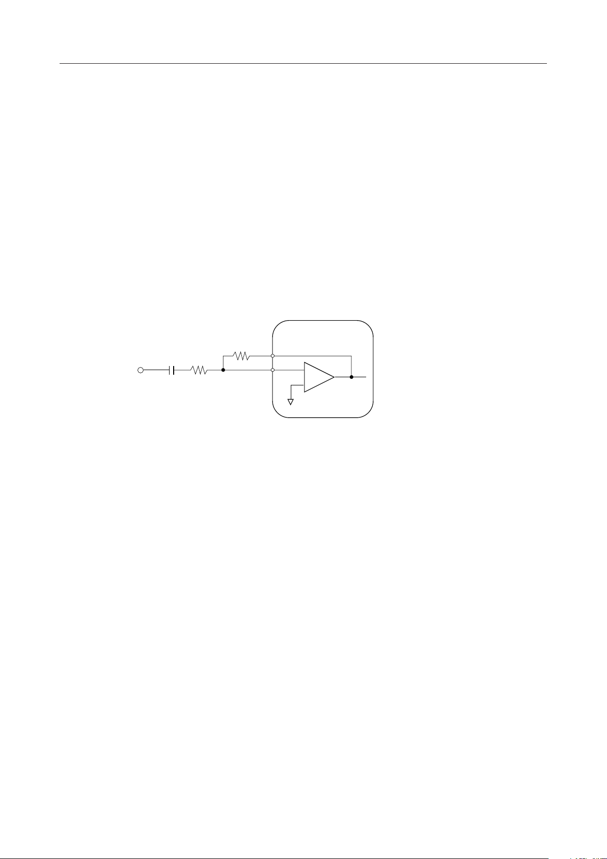
AIN1, AIN2, AIN3, AIN4, GSX1, GSX2, GSX3, GSX4
AIN1, AIN2, AIN3, and AIN4 are the transmit analog inputs for channels 1, 2, 3 and 4
respectively.
GSX1, GSX2, GSX3, and GSX4 are the transmit level adjustments for channels 1, 2, 3 and 4
respectively.
AIN1, AIN2, AIN3, and AIN4 are connected to the inverting inputs for the op-amps. GSX1, GSX2,
GSX3, and GSX4 are connected to the outputs for the op-amps. They are used to adjust levels as
shown below, and are connected to the outputs of the op-amps.
During power saving mode and power down mode, the GSX1, GSX2, GSX3, and GSX4 outputs
are at 0 V.
When these pins are not used, connect AIN1 to GSX1, AIN2 to GSX2, AIN3 to GSX3, and AIN4
to GSX4.
CHn
Analog Input
R2n
C1n R1n
GSXn
AINn
CHn Gain
–
+
Gain = R2n/R1n £ 10
R1n: Variable
R2n > 20 k
C1n > 1/(2 ¥ 3.14 ¥ 30 ¥ R1n) (F)
W
AOUT1, AOUT2, AOUT3, AOUT4
AOUT1, AOUT2, AOUT3, and AOUT4 are the receive filter outputs for channels 1, 2, 3, and 4
respectively.
When the digital signal of +3 dBm0 is input to DIN1, DIN2, DIN3, and DIN4, the output signal
has an amplitude of 3.4 VPP above and below the signal ground voltage (SG : 1/2 VDD). The
output can drive a load of 600 W or more.
During power saving or power down mode, these outputs are at the voltage level of SG with a
high impedance.
4/20
Page 5

¡ Semiconductor MSM7705-01/02/03
DIN1, DIN2, DIN3
PCM signal inputs for channels 1, 2, and 3 when the parallel mode is selected.
D/A conversion is performed by the serial PCM signals to these pins, the RSYNC signals
synchronous with the serial PCM signals, and the BCLK signal. Then the analog signals are
output from AOUT1, AOUT2, and AOUT3 pins, respectively.
The data rate of the PCM signal is equal to the frequency of the BCLK signal.
The PCM signal is shifted at the falling edge of the BCLK signal and latched into the internal
register when shifted by eight bits.
The start of the PCM data (MSD) is identified at the rising edge of RSYNC.
When the serial mode is selected, this pin is not used and should be connected to GND (0 V).
DIN4
PCM signal input for channel 4 when the parallel mode is selected.
D/A conversion is performed by the serial PCM signal to this pin, the RSYNC signal synchronous
with the serial PCM signal, and the BCLK signal. Then the analog signal is output from AOUT4
pin.
The data rate of the PCM signal is equal to the frequency of the BCLK signal.
The PCM signal is shifted at the falling edge of the BCLK signal and latched into the internal
register when shifted by eight bits.
The start of the PCM data (MSD) is identified at the rising edge of RSYNC.
When the serial mode is selected, this pin is used for the 4ch multiplexed PCM signal input.
BCLK
Shift clock signal input for DIN1, DIN2, DIN3, DIN4, DOUT1, DOUT2, DOUT3, and DOUT4.
The frequency is equal to the data rate. Setting this signal to logic "1" or "0" drives both transmit
and receive circuits to the power saving state.
RSYNC
Receive synchronizing signal input.
Eight bits of PCM data required are selected from a series of PCM signal to the DIN1, DIN2, DIN3,
and DIN4 pins by the receive synchronizing signal.
All timing signals in the receive section are synchronized by this synchronizing signal. This
signal must be synchronized in phase with the BCLK (generated from the same clock source as
BCLK). The frequency should be 8 kHz ±50 ppm to guarantee the AC characteristics which are
mainly the frequency characteristics of the receive section.
However, this device operates in the range of 6 kHz to 10 kHz unless the frequency characteristics
of the system used are strictly specified, but the electrical characteristics specified in the data
sheet are not guaranteed.
5/20
Page 6
¡ Semiconductor MSM7705-01/02/03
XSYNC
Transmit synchronizing signal input.
PCM output signal from the DOUT1, DOUT2, DOUT3, and DOUT4 pins is output in
synchronization with this transmit synchronizing signal. This synchronizing signal triggers the
PLL and synchronizes all timing signals of the transmit section.
This synchronizing signal must be synchronized in phase with BCLK.
The frequency should be 8 kHz ±50 ppm to guarantee the AC characteristics which are mainly
the frequency characteristics of the transmit section.
However, this device can be operated in the range of 6 kHz to 10 kHz unless the frequency
characteristics of the system used are strictly specified, but the electrical characteristics are not
guaranteed.
Setting this signal to logic "1" or "0" drives both transmit and receive circuits to power saving
state.
DOUT1
PCM signal output of channel 1 when the parallel mode is selected.
The PCM output signal is output from MSD in a sequential order, synchronizing with the rising
edge of the BCLK signal.
MSD may be output at the rising edge of the XSYNC signal, based on the timing between BCLK
and XSYNC.
This pin is in a high impedance state except during 8-bit PCM output. It is also in a high
impedance state during power-saving state or power-down state.
When the serial mode is selected, this pin is configured to be the output of serial multiplexed 4ch
PCM signal.
A pull-up resistor must be connected to this pin because it is an open drain output.
This device is compatible with the ITU-T recommendation on coding law and output coding
format.
The MSM7705-03 (A-law) outputs the character signal, inverting the even bits.
Input/Output Level
+Full scale
+0
–0
–Full scale
PCMIN/PCMOUT
MSM7705-02 (m-law)
MSD
1000 0000
1111 1111
0111 1111
0000 0000
MSM7705-03 (A-law)
MSD
1010 1010
1101 0101
0101 0101
0010 1010
6/20
Page 7

¡ Semiconductor MSM7705-01/02/03
DOUT2, DOUT3, DOUT4
PCM signal outputs for channels 2, 3, and 4 when parallel mode is selected.
The PCM output signal is output from MSD in a sequential order, synchronizing with the rising
edge of the BCLK signal.
MSD may be output at the rising edge of the XSYNC signal, based on the timing between BCLK
and XSYNC.
This pin is in a high impedance state except during 8-bit PCM output. It is also in a high
impedance state during power-saving state or power-down state.
When the serial mode is selected, this pin is unconnected.
A pull-up resistor must be connected to each of these pins because it is an open drain output.
This device is compatible with the ITU-T recommendation on coding law and output coding
format.
The MSM7705-03 (A-law) outputs the character signal inverting the even bits.
CHPS
Control signal input for the mode selection of PCM input and output.
When this signal is at a logic "1" level, the PCM input and output are in parallel mode. The PCM
data of CH1, CH2, CH3, and CH4 is input to DIN1, DIN2, DIN3, and DIN4 outputs from DOUT1,
DOUT2, DOUT3, and DOUT4 with the same timing.
When this signal is at logic "0" level, the PCM input and output are in serial mode. The PCM data
of CH1 to CH4 is input from DIN4 and output from DOUT1 as time division multiplexed data.
PDN
Power down control signal.
When PDN is at a logic "0" level, both transmit and receive circuits are in power down state.
V
DD
Power supply for +5 V.
A power supply for an analog circuit in the system to which the device is applied should be used.
A bypass capacitor of 0.1 mF to 1 mF with excellent high-frequency characteristics and a capacitor
of 10 mF to 20 mF should be connected between this pin and the AG pin if needed.
AG
Analog signal ground.
DG
Ground for digital signal circuits.
This ground is separate from the analog signal ground. The DG pin must be connected to the AG
pin on the printed circuit board to make a common analog ground.
7/20
Page 8

¡ Semiconductor MSM7705-01/02/03
SGC
Used to generate the signal ground voltage level by connecting a bypass capacitor.
Connect a 0.1 mF capacitor with excellent high frequency characteristics between the AG pin and
the SGC pin.
ALAW
Control signal input of the companding law selection.
Only the MSM7705-01GS-2K has this pin. The CODEC will operate in the m-law when this pin
is at a logic "0" level and will operate in the A-law when this pin is at a logic "1" level. The CODEC
operates in the m-law if the pin is left open, since this pin is internally pulled down.
8/20
Page 9

¡ Semiconductor MSM7705-01/02/03
ABSOLUTE MAXIMUM RATINGS
Parameter
Power Supply Voltage
Analog Input Voltage
Digital Input Voltage
Storage Temperature
Symbol
V
DD
V
AIN
V
DIN
T
STG
Condition
—
—
—
—
RECOMMENDED OPERATING CONDITIONS
Parameter
Power Supply Voltage
Operating Temperature
Analog Input Voltage
High Level Input Voltage
Low Level Input Voltage
Clock Frequency
Sync Pulse Frequency
Clock Duty Ratio
Digital Input Rise Time
Digital Input Fall Time
Transmit Sync Pulse Setting Time
Receive Sync Pulse Setting Time
Sync Pulse Width
DIN Setup Time
DIN Hold Time
Digital Output Load
Analog Input Allowable DC Offset
Allowable Jitter Width
Symbol
V
DD
Ta
V
AIN
V
IH
V
IL
F
C
F
S
D
C
t
Ir
t
If
t
XS
t
SX
t
RS
t
SR
t
WS
t
DS
t
DH
R
DL
C
DL
V
off
—
Condition
Voltage must be fixed
—
Gain = 1
XSYNC, RSYNC, BCLK, DIN1,
DIN2, DIN3, DIN4, PDN,
CHPS, ALAW
BCLK = (When in 4ch serial
mode, 64, 96, 128, 192 kHz
are not used)
XSYNC, RSYNC
BCLK
XSYNC, RSYNC, BCLK, DIN1,
DIN2, DIN3, DIN4, PDN, CHPS
BCLKÆXSYNC, See Fig. 1
XSYNCÆBCLK, See Fig. 1
BCLKÆRSYNC, See Fig. 1
RSYNCÆBCLK, See Fig. 1
XSYNC, RSYNC
DIN1, DIN2, DIN3, DIN4
DIN1, DIN2, DIN3, DIN4
DOUT1, DOUT2,
DOUT3, DOUT4
Pull-up resistor
Transmit gain stage, Gain = 1
Transmit gain stage, Gain = 10
XSYNC, RSYNC
—
Rating
0 to 7.0
–0.3 to V
–0.3 to V
DD
DD
+ 0.3
+ 0.3
–55 to +150
Min.
4.75
–30
—
2.2
0
Typ.
5.0
+25
—
—
—
Max.
64, 128, 256, 512, 1024,
2048, 96, 192, 384, 768,
1536, 1544
6.0
40
—
—
100
100
100
100
1 BCLK
100
100
0.5
—
VDD/2 –100
VDD/2 –10
—
8.0
50
—
—
—
—
—
—
—
—
—
—
—
—
—
—
VDD/2 +100
VDD/2 +10
5.25
+85
3.4
V
DD
0.8
10.0
60
50
50
—
—
—
—
100
—
—
—
100
500
Unit
V
V
V
°C
Unit
V
°C
V
PP
V
V
kHz
kHz
%
ns
ns
ns
ns
ns
ns
ms
ns
ns
kW
pF
mV
mV
ns
9/20
Page 10

¡ Semiconductor MSM7705-01/02/03
ELECTRICAL CHARACTERISTICS
DC and Digital Interface Characteristics
(V
= +5 V ±5%, Ta = –30°C to +85°C)
DD
Parameter
Power Supply Current
Symbol
I
DD1
I
DD2
Condition
Operating mode, No signal
Power-save mode, PDN = 1,
XSYNC or BCLK OFF
Min.
—
—
Typ.
14.0
2.6
Max.
28.0
6.0
Unit
mA
mA
Power-down mode, PDN = 0
I
DD3
BCLK OFF
High Level Input Voltage
Low Level Input Voltage
High Level Input Leakage Current
Low Level Input Leakage Current
Digital Output Low Voltage
Digital Output Leakage Current
Input Capacitance
V
IH
V
IL
I
IH
I
IL
V
Pull-up resistor > 500 W
OL
I
O
C
IN
Transmit Analog Interface Characteristics
Parameter
Input Resistance
Output Load Resistance
Output Load Capacitance
Output Amplitude
Offset Voltage
Symbol
R
INX
R
LGX
C
LGX
V
OGX
V
OSGX
AIN1, AIN2, AIN3, AIN4
GSX1, GSX2, GSX3, GSX4
with respect to SG
mA
V
V
mA
mA
V
mA
—
—
—
—
—
—
2.2
0.0
—
—
0.0
—
0.01
—
—
—
—
0.2
—
0.05
V
DD
0.8
2.0
0.5
0.4
10
— —5—pF
(V
= +5 V ± 5%, Ta = –30°C to +85°C)
DD
Condition Min. Typ. Max. Unit
Gain = 1
10
20
—
–1.7
–20
—
—
—
—
—
—
—
30
+1.7
+20
MW
kW
pF
V
mV
Receive Analog Interface Characteristics
Parameter
Output Load Resistance
Output Load Capacitance
Output Amplitude
Offset Voltage
Symbol
R
LAO
C
LAO
V
OAO
V
OSAO
AOUT1
AOUT2
AOUT3
AOUT4
(V
= +5 V ±5%, Ta = –30°C to +85°C)
DD
Condition Min. Typ. Max. Unit
Each output;
0.6
—
—
kW
with respect to SG
= 0.6 kW;
R
L
—
—
–1.7
—
—
50
+1.7
pF
V
with respect to SG
—
–100
—
+100
mV
10/20
Page 11

¡ Semiconductor MSM7705-01/02/03
AC Characteristics
(V
= +5 V ±5%, Ta = –30°C to +85°C)
DD
Parameter
Transmit Frequency Response
Receive Frequency Response
Transmit Signal to Distortion Ratio 1020 dB
Receive Signal to Distortion Ratio 1020 dB
Transmit Gain Tracking
Receive Gain Tracking
Symbol
Loss T1
Loss T2
Loss T3
Loss T4
Loss T5
Loss T6
Loss R1
Loss R2
Loss R3
Loss R4
Loss R5
SD T1 35 43 —3
SD T2 35 41 —0
SD T3 35 38 —–30
SD T4 29 31.5 —–40
SD T5 24 27 —–45
SD R1 36 43 —3
SD R2 36 41 —0
SD R3 36 40 —–30
SD R4 30 33.5 —–40
SD R5 25 30 —–45
GT T1 –0.3 +0.02 +0.3
GT T2 Reference
GT T3 1020 –0.3 +0.04 +0.3 dB–40
GT T4 –0.5 +0.15 +0.5
GT T5 –1.2 +0.40 +1.2
GT R1 –0.3 0.0 +0.3
GT R2 Reference
GT R3 1020 –0.3 +0.04 +0.3 dB
GT R4 –0.5 +0.16 +0.5
GT R5 –1.2 +0.37 +1.2
Freq.
(Hz)
60 20 26 —
300 –0.15 +0.07 +0.20
1020 Reference
2020 –0.15 –0.04 +0.20
3000 –0.15 +0.03 +0.20
3400 0 0.40 0.80
300 –0.15 –0.03 +0.20
1020 Reference
2020 –0.15 +0.04 +0.20 dB0
3000 –0.15 +0.11 +0.20
3400 0.0 0.47 0.80
Level
(dBm0)
3
–10
–50
–55
3
–10
–40
–50
–55
Condition
*1
*1
Min. Typ. Max. Unit
dB0
*1 Psophometric filter is used
11/20
Page 12

¡ Semiconductor MSM7705-01/02/03
AC Characteristics (Continued)
(V
= +5 V ±5%, Ta = –30°C to +85°C)
DD
Parameter
Idle Channel Noise
Absolute Level (Initial Difference)
Absolute Level
(Deviation of Temperature and Power)
Absolute Delay
Transmit Group Delay
Receive Group Delay
Crosstalk Attenuation
Symbol
Freq.
(Hz)
Nidle T
Nidle R
—
— –78
AV T 0.821 0.850 0.880
Level
(dBm0)
—
—
Condition
AIN = SG
*1 *2
*1 *3
V
= 5.0 V
DD
Min. Typ. Max. Unit
—
—
–73.5
–71.5
–70
–68
— –75
Ta = 25°C
AV R 0.821 0.850 0.880
AV Tt –0.2 — +0.2
1020
0
V
DD
= 5 V
±5%
Ta = –30
AV Rt –0.2 — +0.2
to +85°C
A to A
t
D
1020 — — 0.60 ms0
BCLK
= 64 kHz
T1 — 0.19 0.75
t
GD
tGD T2 — 0.11 0.35
tGD T3 — 0.02 0.1250
T4 — 0.05 0.125
t
GD
T5 — 0.75
GD
tGD R1
t
R2
GD
t
R3
GD
R4
t
GD
t
R5
GD
CR T 7580—
CR R 76
500
600
1000
2600
2800
500
600
1000
2600
2800
1020 dB0
*4
*4
TRANS Æ RECV
RECV Æ TRANS
0.07t
— 0.00 0.75
— 0.35
0.00
— 0.00 0.125 ms0
— 0.09 0.125
— 0.12 0.75
70 —
CR CH 80CH to CH 75 —
dBm0p
Vrms
dB
dB
ms
*1 Psophometric filter is used
*2 Upper columns are specified for the m-law, lower for the A-law
*3 Input "0" code to PCMIN
*4 Minimum value of the group delay distortion
12/20
Page 13

¡ Semiconductor MSM7705-01/02/03
AC Characteristics (Continued)
(V
= +5 V ±5%, Ta = –30°C to +85°C)
DD
Parameter
Symbol
Freq.
(Hz)
Level
(dBm0)
4.6 kHz to
Discrimination 0
DIS
72 kHz
300 to
S
3400
fa = 470
IMD
fd = 320
Digital Output Delay Time
PSR T
PSR R
t
SD
t
XD1
t
XD2
t
XD3
0 to
50 kHz
PP
CL = 100 pF + 1 LSTTL
*5 Measurement performed under idle channel noise
Condition
0 to
4000 Hz
4.6
kHz
to
100 kHz
*5
Min. Typ. Max. Unit
30 32 — dB
— –37.5 –35 dBm0Out-of-band Spurious 0
— –52 –35 dBm0Intermodulation Distortion –4 2fa – fd
—30—dBPower Supply Noise Rejection Ratio 50 mV
20 — 200
20 — 200
ns
20 — 200
20 — 200
13/20
Page 14

¡ Semiconductor MSM7705-01/02/03
TIMING DIAGRAM
Transmit Timing
BCLK 12345678910
XSYNC
t
XS
t
SX
t
WS
DOUT1
DOUT2
DOUT3
DOUT4
t
XD1
t
SD
D2
t
XD2
t
XD3
D3 D4 D5 D6 D7 D8MSD
Transmit Side
Receive Timing
BCLK 12345678910
RSYNC
DIN1
DIN2
DIN3
DIN4
t
RS
t
SR
t
WS
D2
t
DS
t
DH
D3 D4 D5 D6 D7MSD
D8
Receive Side
11
11
BCLK
XSYNC
DOUT1
BCLK
RSYNC
DIN4
Figure 1 Timing Diagram in the Parallel Mode (CHPS = 1)
MSD
D2 D3 D4 D5 D6 D7 D8
CH1 PCM Data
MSD
D2 D3 D4 D5 D6 D7 D8
CH1 PCM Data
MSD
D2 D3 D4 D5 D6 D7 D8
CH2 PCM Data
MSD
D2 D3 D4 D5 D6 D7 D8
CH2 PCM Data
MSD
D2 D3 D4 D5 D6 D7 D8
Transmit Side
MSD
D2 D3 D4 D5 D6 D7 D8
MSD
D2 D3 D4 D5 D6 D7 D8
CH3 PCM Data
MSD
D2 D3 D4 D5 D6 D7 D8
CH3 PCM Data
CH4 PCM Data
CH4 PCM Data
Receive Side
Figure 2 Timing Diagram in the Serial Mode (CHPS = 0)
14/20
Page 15

¡ Semiconductor MSM7705-01/02/03
APPLICATION CIRCUIT
Example of Basic Connection (PCM Serial Mode Operation)
+5 V
CH1
Analog Input
CH1
Analog Output
1 mF 20 kW
1 mF
20 kW
MSM7705-01
AIN1
GSX1
AOUT1
DOUT1
DOUT2
DOUT3
DOUT4
1 kW
(Open)
(Open)
(Open)
4ch Multiplex PCM
Signal Output
CH2
Analog Input
CH2
Analog Output
CH3
Analog Input
CH3
Analog Output
CH4
Analog Input
CH4
Analog Output
0 V
+5 V
0 to 20 W
1 mF 20 kW
1 mF
1 mF 20 kW
1 mF
1 mF 20 kW
1 mF
10 mF1 mF
20 kW
20 kW
20 kW
0.1 mF
+
AIN2
GSX2
AOUT2
AIN3
GSX3
AOUT3
AIN4
GSX4
AOUT4
SGC
AG
AG
DG
DG
DIN4
DIN3
DIN2
DIN1
BCLK
XSYNC
RSYNC
PDN
ALAW
CHPS
V
DD
V
DD
4ch Multiplex PCM
Signal Input
0 V
Bit Clock Input
Sync Pulse Input
Power Down Control Input
1 : Operation
0 : Power Down
Companding Law Control Input
1 : A-law
0 : m-law
0 V
15/20
Page 16

¡ Semiconductor MSM7705-01/02/03
APPLICATION INFORMATION
DOUT Pull-up Resistor
A value of the pull-up resistor for the DOUT pin should be determined depending on frequencies
of BCLK and load capacitance.
If a smaller value is used, there may be some degradation in noise performance, resulting in an
increase in supply current.
Equation to give pull-up resistor
1
BCLK
C
L
– 50 ns
————
Rpull = ———————— (W)
4 ¥ f
where
f
50 ns =
Frequency of BCLK
=
BCLK
Load capacitance of the PCMOUT pin
C
=
L
(approximately 20 pF for a CMOS or TTL load)
Internal delay of the MSM7705
Condition for Calculation
If data is turned back from DOUT to DIN under the condition the SYNC signal and BCLK signal
rise simultaneously, the data can normally be transferred.
X, RSYNC
BCLK
T
T = Rpull ¥ C
L
DOUT
16/20
Page 17

¡ Semiconductor MSM7705-01/02/03
Calculation Example for Typical Values
95.2
46.3
21.9
9.7
5.6
3.6
Rpull (kW)
CL = 50 pF
77.1
38.1
18.5
8.8
3.9
2.2
1.4
CL = 100 pF
38.6
19.0
9.3
4.4
1.9
1.1
0.7
BCLK (kHz)
64
128
256
512
1024
1544
2048
= 10 pF
C
L
385.6
190.3
92.7
43.8
19.4
11.2
CL = 20 pF
192.8
7.2
Choice of Actual Resistor Value
If the calculated value is more than or equal to 100 kW, 100 kW should be employed. +10% of the
calculated value is within a tolerance, thus, for example, the value of 10 kW can be used for the
calculated value of 9.3 kW in the above examples.
Channel Crosstalk
The MSM7705 contains the 4-channel CODEC. The circuit and trace design and pin layout are
made to minimize crosstalk between channels inside the LSI device provided the following
should be taken into consideration.
Transmit side
The GSX1 – AIN2, AIN3, and AIN4 traces should not be kept closer.
The GSX2 – AIN1, AIN3, and AIN4 traces should not be kept closer.
The GSX3 – AIN1, AIN2, and AIN4 traces should not be kept closer.
The GSX4 – AIN1, AIN2, and AIN3 traces should not be kept closer.
AIN1, AIN2, AIN3, and AIN4, which are op-amp inverting input pins, have higher resistance,
therefore proximity of these lines to signal lines of other channels may cause crosstalk.
Receive side
The channel outputs AOUT1, AOUT2, AOUT3, and AOUT4 of the receive side are amplifier
outputs with lower resistance, thus crosstalk due to PCB traces is smaller. Nevertheless, the
PCB traces should not be run closer together and in parallel wherever possible.
17/20
Page 18

¡ Semiconductor MSM7705-01/02/03
How to Avoid Transmit Side Amplifier Oscillation Due to PCB Layout
AINn
R
F
GSXn
–
+
MSM7705
The trace length (illustrated by the bold line in the above drawing) should be kept as short as
possible in order to avoid oscillation.
The length of less than 2 cm or 3 cm is permissible, though it depends on PCB layout.
It is recommended to connect a capacitor of 20 pF to 50 pF across the feedback resistor RF, if the
oscillation occurs.
18/20
Page 19

¡ Semiconductor MSM7705-01/02/03
NOTES ON USED
• To ensure proper electrical characteristics, use bypass capacitors with excellent high frequency
characteristics for the power supply and keep them as close as possible to the device pins.
• Connect the AG pin and the DG pin as close as possible. Connect to the system ground with
low impedance.
• Mount the device directly on the board when mounted on PCBs. Do not use IC sockets. If the
use of IC socket is unavoidable, use the short lead type socket.
• When mounted on a frame, use electro-magnetic shielding, if any electro-magnetic wave
sources such as power supply transformers surround the device.
• Keep the voltage on the VDD pin not lower than –0.3 V even instantaneously to avoid latchup that may otherwise occur when power is turned on.
• Use a low noise (particularly, low level type of high frequency spike noise or pulse noise)
power supply to avoid erroneous operation and the degradation of the characteristics of these
devices.
19/20
Page 20

¡ Semiconductor MSM7705-01/02/03
PACKAGE DIMENSIONS
(Unit : mm)
QFP44-P-910-0.80-2K
Mirror finish
Package material
Lead frame material
Pin treatment
Solder plate thickness
Package weight (g)
Epoxy resin
42 alloy
Solder plating
5 mm or more
0.41 TYP.
Notes for Mounting the Surface Mount Type Package
The SOP, QFP, TSOP, SOJ, QFJ (PLCC), SHP and BGA are surface mount type packages, which
are very susceptible to heat in reflow mounting and humidity absorbed in storage.
Therefore, before you perform reflow mounting, contact Oki’s responsible sales person for the
product name, package name, pin number, package code and desired mounting conditions
(reflow method, temperature and times).
20/20
 Loading...