

Page 1

E2F0009-18-62
Preliminary
¡ Semiconductor MSM7661B
This version: Jun. 1998
¡ Semiconductor
MSM7661B
NTSC/PAL Digital Video Decoder
GENERAL DESCRIPTION
The MSM7661B is an LSI device which converts digitally sampled NTSC or PAL video signals
to 8-bit format based on ITU-RBT601.
The input video signals available are composite video signals and S video signals.
The composite video signals are converted to YUV data via a 2-dimensional Y/C separation
circuit.
The A-to-D converted data is data sampled at pixel clock frequency or double pixel clock
frequency (the built-in decimation filter is used). Input signal synchronization can lock
synchronization and color burst at high speed through internal digital processing.
The MSM7661B is upward compatible with the MSM7661. It provides additional features which
are added to the MSM7661 indicated by the mark n and is superior to the MSM7661 in picture
quality and synchronization stability. The device, which includes an additional register added
to the MSM7661, has electrical characteristics which are nearly equal to those of the MSM7661.
The MSM7661B allows a pin-for-pin replacement with the MSM7661.
FEATURES (• indicates a new feature compared with MSM7660. n indicates a
new feature compared with MSM7661.)
• Input video signals include the following two types of digital data that are A-to-D converted
at pixel frequency or double pixel frequency :
NTSC/PAL composite video signal
NTSC/PAL S video signal
8-bit Y/8-bit C (CbCr) output (conforms to ITU-RBT601)
°
YCbCr 4 : 2 : 2
YCbC4 : 1 : 1
n YCbCr 8-bit multiplex output (27 MHz) (not including SAV and EAV)
• 2-dimensional Y/C separation using adaptive comb filter (this filter is bypassed for S video
signal input)
NTSC: 3 lines/2 lines
PAL: 2 lines (3 virtual lines)
• Input signal synchronization can lock synchronization and color burst at high speed through
internal digital processing.
Sampling frequency
°
13.5 MHz (ITU-R601)
12.27 MHz (NTSC Square Pixel)
14.31818 MHz (NTSC 4Fsc)
14.75 MHz (PAL Square Pixel)
• Internal AGC/ACC circuit
Switchable between AGC and MGC (fixed gain)
n Switchable between ACC and MCC (fixed gain)
• Built-in decimation filter located in the input stage allows easy configuration of an external
filter circuit (located ahead of A/D converter).
• Automatic NTSC/PAL recognition (only for ITU-RBT.601)
• Sleep mode
1/42
Page 2

¡ Semiconductor MSM7661B
• Multiplex signal recognition (Teletext)
Data during vertical blanking is output in 8 bits in Through mode.
I2C-bus interface
°
• 3.3 V single power supply (each I/O pin is 5 V tolerable)
• Package:
64-pin plastic QFP (QFP64-P-1414-0.80-BK) (Product name: MSM7661B GS-BK)
2/42
Page 3
¡ Semiconductor MSM7661B
3/42
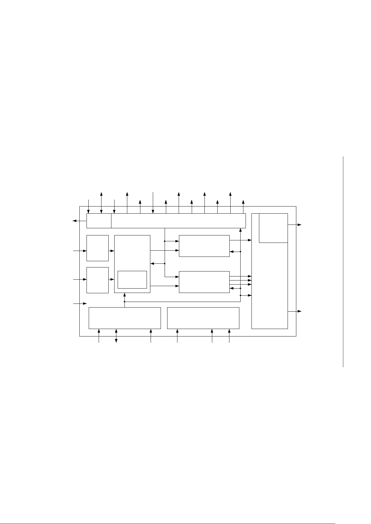
BLOCK DIAGRAM
SCL
Synchronization Block
Luminance Block
(AGC + LPF)
Prologue Block
lum.
chr.
Decimation
Filter
Line Memory
(1kbyte) ¥ 2
(2Dim. Y/C separate)
Chrominance Block
(ACC + LPF)
I2C-bus Control Logic Test Control Logic
Epilogue
Block
(Output Formatter)
SDA RESET_L TE TEST1 TEST2
(SLEEP)
ODDCLKX2PLLSEL
VVALID
HVALID
VSYNC_L
HSYNC_L
HSYCLKX2O
SYSSEL
CLKSEL
CLKXO
MODE[3:0]
YD[7:0]
VCO_CP
CD[7:0]
Y[7:0]
8 bits
(YCbCr)
C[7:0]
SYNC
(CSYNC_L)
Decimation
Filter
Page 4
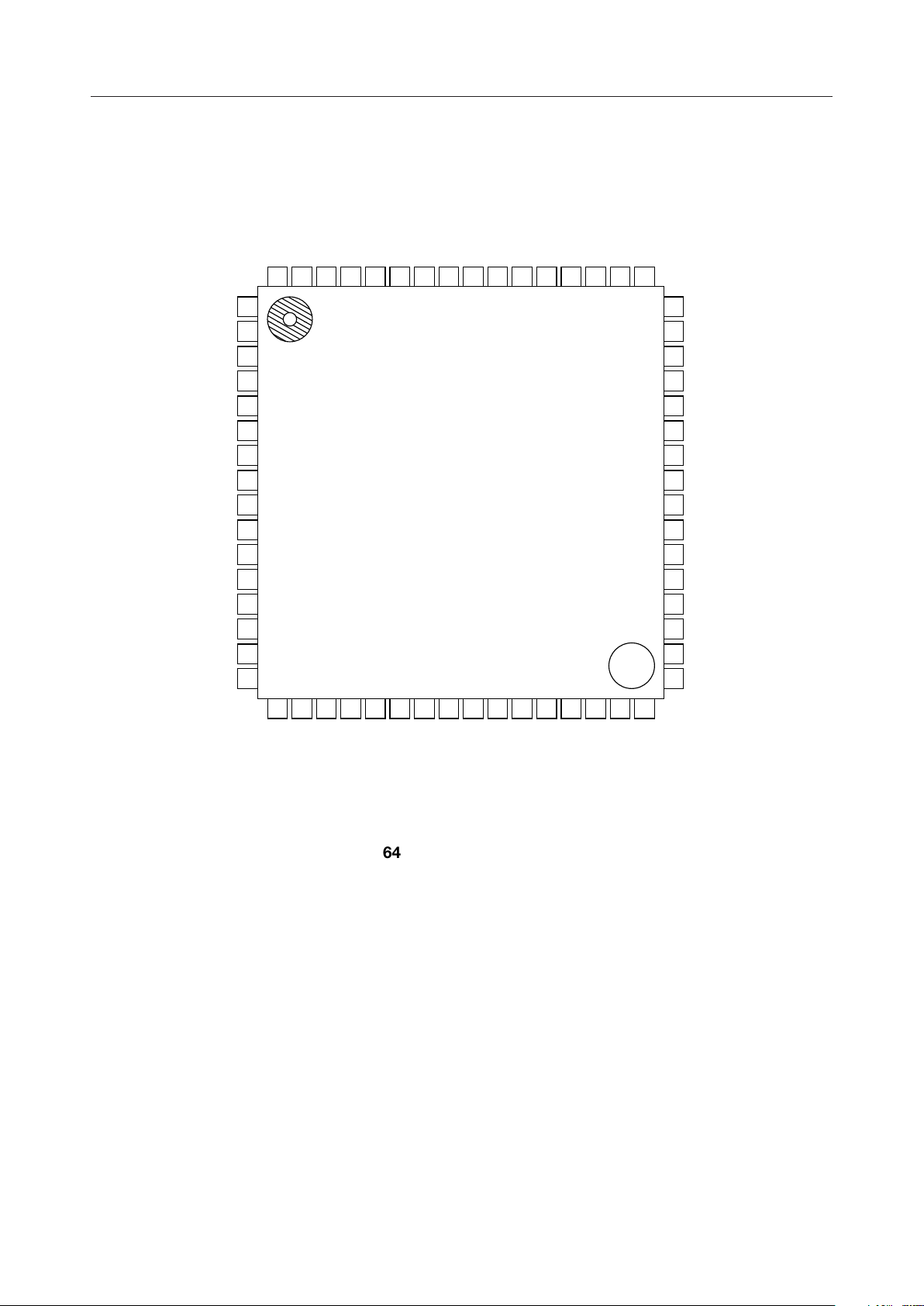
¡ Semiconductor MSM7661B
PIN CONFIGURATION (TOP VIEW)
CD[0]
CD[1]
CD[2]
CD[3]
CD[4]
CD[5]
CD[6]
CD[7]
CVBS[0]
CVBS[1]
CVBS[2]
CVBS[3]
CVBS[4]
CVBS[5]
CVBS[6]
CVBS[7]
10
11
12
13
14
15
16
1
2
3
4
5
6
7
8
9
VDDGND
644963
CLKX2
HSY
62
61
SYNC
60
VCO_CP
CLKX2O
59
58
SYSSEL
CLKXO
57
56
HSYNC_L
VSYNC_L
HVALID
55
54
53
VVALID
ODD
52
51
GND
50
V
DD
48
47
46
45
44
43
42
41
40
39
38
37
36
35
34
33
C[0]
C[1]
C[2]
C[3]
C[4]
C[5]
C[6]
C[7]
Y[0]
Y[1]
Y[2]
Y[3]
Y[4]
Y[5]
Y[6]
Y[7]
173218
DD
V
GND
19
SCL
20
21
22
23
24
SDA
MODE[0]
MODE[1]
MODE[2]
MODE[3]
64-Pin Plastic QFP
25
26
PLLSEL
RESET_L
27
28
TEST1
CLKSEL
29
30
TE
SLEEP
31
GND
V
DD
4/42
Page 5
¡ Semiconductor MSM7661B
PIN DESCRIPTIONS
Pin
1 to 8
Symbol
CD[0 to 7]
Type
I
Chrominance signal input pin (valid only for S video input)
Description
Set each pin to "L" level at composite signal input.
9 to 16
CVBS[0 to 7]
Composite signal input pin
I
Luminance signal is input for S video input.
17
18
19
20
21 to 24
V
DD
GND
SCL
SDA
MODE[0 to 3]
2
I
C-bus clock pin
I
2
C-bus data pin
I
I/O
Mode input pins. These pins are internally pulled-down.
I
MODE[3] 0: composite
MODE[2] 0: NTSC
1: S video
MODE[1:0] 00: ITU-R601
01: Square Pixel
10: 4Fsc (only for NTSC)
11: none
If ITU-R signals are input when registers are set to automatic NTSC/PAL
recognition mode, NTSC/PAL is automatically recognized irrespective of
MODE2 setting.
25 IRESET_L
26
PLLSEL
System reset pin (active at "L")
Unused.
I
Fixed to "H" externally.
27
CLKSEL
Clock select input pin.
I
"L" Æ double-speed 27 MHz, "H" Æ ordinary 13.5 MHz
28
29
TEST1
SLEEP
Input pin for testing. Normally "L". Internally pulled down.
I
Sleep mode setting pin. Normally "L". Internally pulled down.
I
30 ITE Input pin for testing. Normally "L". Internally pulled down.
31 GND
32 V
DD
1: PAL
5/42
Page 6
¡ Semiconductor MSM7661B
Pin
33 to 40
41 to 48
49
50
51
52
53
54
55
56
57
58
59
64
Symbol
Y[7 to 0]
C[7 to 0]
V
DD
GND
ODD
VVALID
HVALID
VSYNC_L
HSYNC_L
CLKXO
SYSSEL
CLKX2O
VCO_CP
SYNC I/O60
GND63
V
DD
Type
O
O
O
O
O
O
O
O
O
O
O
Description
Chrominance signal output pins
YCbCr 8-bit multiplex output pins
Luminance signal output pins
Field display output pin
Outputs "H" for odd field.
Vertical valid line timing output pin
Horizontal valid pixel timing output pin
V sync output pin
H sync output pin
Internal operation clock output pin
Display select output pin for NTSC-PAL detect / multiplex signal detect /
HLOCK sync detect.
Selection by register. (Default : NTSC-PAL detect)
NTSC mode : "L", PAL mode : "H"
Multiplex signal detect : "H"
HLOCK sync detect : "H"
Clock output pin
Unused.
Open normally.
Composite sync output.
Unused as input pin.
Clamp signal timing output pin for A/D converterHSY O61
Clock input pinCLKX2 I62
6/42
Page 7
¡ Semiconductor MSM7661B
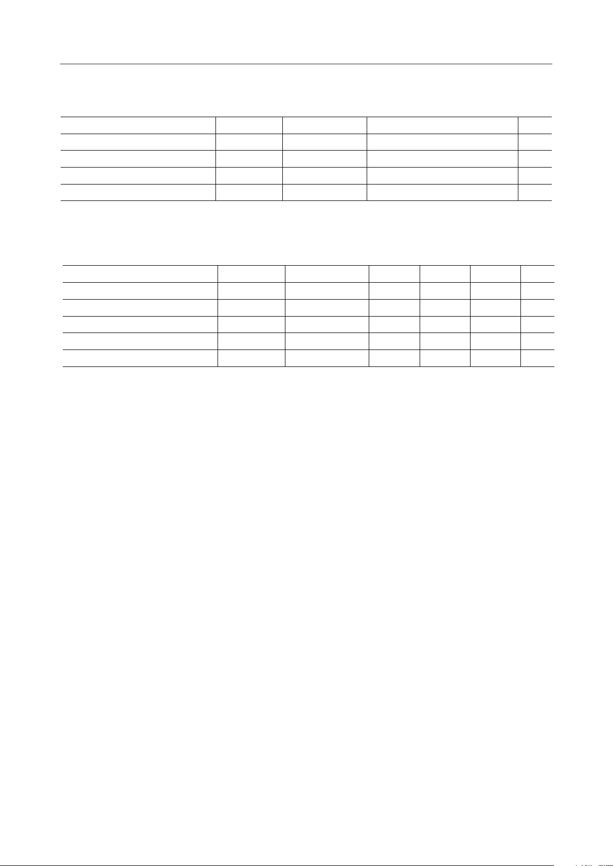
ABSOLUTE MAXIMUM RATINGS
Parameter
Power Supply Voltage
Input Voltage
Power Consumption
Storage Temperature
Symbol
V
DD
V
I
P
W
T
STG
Condition
—
—
—
—
Rating
–0.3 to +4.5
–0.3 to +5.5
800
–55 to +150
RECOMMENDED OPERATING CONDITIONS
Parameter
Power Supply Voltage
Power Supply Voltage
"H" Level Input Voltage
"L" Level Input Voltage
Symbol
V
DD
GND
V
IH
V
IL
Condition
—
—
—
—
Operating Temperature Ta — 25 °C
Min.
3.0
—
2.2
0
0
Typ.
3.3
0
—
—
Max.
3.6
—
V
DD
0.8
70
Unit
V
V
mW
°C
Unit
V
V
V
V
7/42
Page 8
¡ Semiconductor MSM7661B
ELECTRICAL CHARACTERISTICS
DC Characteristics
(Ta = 0 to 70°C, VDD = 3.3 V ±0.3 V)
Parameter Symbol
Condition
Min.
Typ.
IOH = –4 mA (*1)
DD
0.7 V
DD
—
–10 +10
—
—V
—
—20 250
"H" Level Output Voltage V
"L" Level Output Voltage V
Input Leak Current I
V
OH
OL
I
IOH = –6 mA (*2)
= –8 mA (*3)
I
OH
= 4 mA (*1)
I
OL
= 6 mA (*2)
I
OL
I
= 8 mA (*3)
OL
VI =
GND to V
R
pull-down
=
50 kW (*4)
Output Leak Current I
Power Supply Current (operating)
I
DDO
O
VI =
CLK
V
GND to V
=
27 MHz
=
3.3 V
DD
DD
— mA–10 +10
155 mA— 190
CLK = 13.5 MHz
Power Supply Current (operating)
Power Supply Current (SLEEP) I
DDO2
DDS
SDA Output Voltage SDAV
SDA Output Current SDAI
=
3.3 V
V
DD
SLEEP ON 1 mA—5
L
O
——V0 0.4
——mA3—
125 mA— 160I
Max.
—
0.4
Unit
mA
*1: HSYNC_L, VSYNC_L, SYSSEL
*2: Y[7:0], C[7:0], HSY, HVALID, VVALID, ODD, CLKXO
*3: CLKX2O
*4: MODE[3:0], SLEEP, TEST1, TE
8/42
Page 9
¡ Semiconductor MSM7661B
(
)
(
)
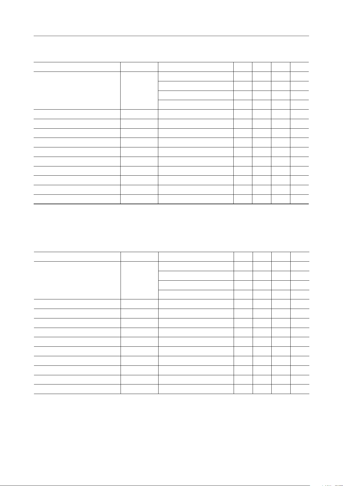
AC Characteristics (Single Speed Mode)
Parameter Symbol Condition Min. Typ. Max. Unit
CLKX2 Cycle Time t
CLKX2 Duty t
Input Data Setup Time t
Input Data Hold Time t
Output Data Delay Time 1 (*) t
Output Data Delay Time 2 (*) t
Output Data Delay Time 3 (*) t
Output Clock Delay Time (*) (External)
Output Clock Delay Time (*) (Internal)
SCL Clock Cycle Time t
Low Level Cycle t
CLKX1
D_D1
IS1
IH1
ODX1
OD2X1
OD1
t
CXD1
t
CD1
C_SCL
L_SCL
(Ta = 0 to 70°C, VDD = 3.3 V ±0.3 V)
ITU-R601 — 74.07 — ns
NTSC 4Fsc — 69.84 — ns
NTSC Square Pixel — 81.5 — ns
PAL Square Pixel — 67.8 — ns
— 40—60%
CLKSEL : H 0 — — ns
CLKSEL : H 30 — — ns
CLKSEL : H 2 — 8 ns
CLKSEL : H 2 — 7 ns
CLKSEL : H 9 — 25 ns
CLKSEL : H 7 — 17 ns
CLKSEL : H 7 — 18 ns
Rpull_up = 4.7 kW 200 — — ns
Rpull_up = 4.7 kW 100 — — ns
*output load 40 pF
AC Characteristics (Double Speed Mode)
Parameter Symbol Condition Min. Typ. Max. Unit
CLKX2 Cycle Time t
CLKX2 Duty t
Input Data Setup Time t
Input Data Hold Time t
Output Data Delay Time 1 (*) t
Output Data Delay Time 2 (*) t
Output Data Delay Time 3 (*) t
Output Clock Delay Time (*) (External)
Output Clock Delay Time (*) (Internal)
SCL Clock Cycle Time t
Low Level Cycle t
CLKX2
D_D2
IS2
IH2
ODX2
OD2X2
OD2
t
CXD2
t
CD2
C_SCL
L_SCL
(Ta = 0 to 70°C, VDD = 3.3 V ±0.3 V)
ITU-R601 — 37.05 — ns
NTSC 4Fsc — 34.9 — ns
NTSC Square Pixel — 40.75 — ns
PAL Square Pixel — 33.9 — ns
— 40—60%
CLKSEL : L 5 — — ns
CLKSEL : L 15 — — ns
CLKSEL : L 2 — 7 ns
CLKSEL : L 2 — 6 ns
CLKSEL : L 9 — 24 ns
CLKSEL : L 7 — 17 ns
CLKSEL : L 7 — 18 ns
Rpull_up = 4.7 kW 200 — — ns
Rpull_up = 4.7 kW 100 — — ns
*output load 40 pF
9/42
Page 10
¡ Semiconductor MSM7661B
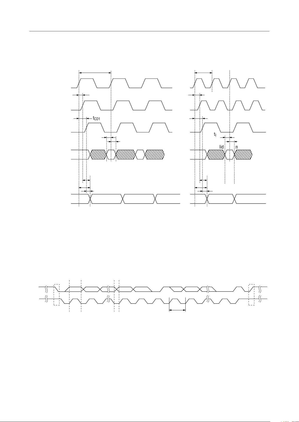
Input and Output Timing
CLKX2
CLKX2O
CLKXO
CVBS
CD
RESET_L
HSY,
HVALID, VVALID,
ODD, SYSSEL,
Y,C,
HSYNC_L,
VSYNC_L
t
OD1
CLKSEL:H
t
CLKX1
t
CXD1
t
CD1
t
IS1
t
IH1
not valid not valid
t
OD2X1
t
ODX1
t
OD2
CLKSEL:L
t
CLKX2
t
CXD2
t
CD2
t
IS2
not valid not valid
t
OD2X2
t
ODX2
t
IH2
I2C-bus Interface Input/Output Timing
The basic input/output timing of the I2C-bus interface is as follows.
SDA
SCL
S
Start Condition
Data Line Stable: Data Valid Change of Data Allowed
MSB
12 789
ACK
12
t
C_SCL
I2C-bus Basic Input/Output Timing
3-8
9
ACK
P
Stop Condition
10/42
Page 11

¡ Semiconductor MSM7661B
BLOCK DESCRIPTION
1. Prologue Block
The prologue block performs Y/C separation by inputting data.
Data can be input either at ordinary pixel frequency (ITU-R : 13.5 MHz) or at double pixel
frequency (ITU-R: 27 MHz).
When the double pixel frequency is used, data is processed after changing to the ordinary pixel
frequency via a decimeter circuit.
By changing the register setting, the decimeter circuit can be bypassed irrespective of whether
data is input at ordinary pixel frequency or at double pixel frequency.
The prologue block performs Y/C separation using a 2-dimensional adaptive comb filter when
composite signals (CVBS) are input.
The following operation modes can be changed via the I2C-bus. The * mark indicates a default.
The default is a state that is selected when reset.
1) Video input mode select
Composite video input *
S video input
2) Video input mode select
Auto NTSC/PAL select* (Only for ITU-R601)
Dependent on Operation mode selected
When ITU-R601 is selected, the video input mode is automatically determined by the number
of lines per field.
3) Operation mode select
NTSC CCIR601 13.5 MHz*
MTSC Square Pixel 12.27 MHz
NTSC 4Fsc 14.31818 MHz
PAL CCIR601 13.5 MHz
PAL Square Pixel 14.75 MHz
4) Decimeter circuit pass/bypass select
Decimeter circuit is passed. *
Decimeter circuit is bypassed.
5) Y/C separation mode select
Adaptive comb filter is used. *
Unadaptive comb filter is used.
Trap filter is used.
The adaptive comb filter detects the correlation up to 3 lines between continuous lines. The Y/
C is separated by the comb filter according to the way of correlation if theses lines are correlated.
The Y/C is separated by the trap filter if these lines are not correlated (only 2 lines in the case of
PAL).
In the unadaptive comb filter, the Y/C is always separated by removing the luminance
component based on the average of preceding and following lines (when there is the correlation
between 3 lines).
11/42
Page 12

¡ Semiconductor MSM7661B
If the comb filter is not used, the Y/C is separated by the trap filter.
The Y/C separation circuit is bypassed by S video signal input.
In adittion, the functions of this block work only when lines are valid as image information.
The processing of CVBS signals is not made during V-blanking.
2. Luminance Block
The luminance block removes synchronous signals from the signals containing luminance
components after Y/C separation. The signals are corrected and output as luminance signals.
The luminance signal output level gain control functions include three selectable modes such as
AGC (Auto Gain Control), MGC (manual Gain Control) + No Clamp, and MGC + Pedestal
Clamp.
In the AGC mode, the luminance level amplification is determined by comparing the depth of
SYNC with the reference value. The default is 40IRE which can be changed by the register. The
input is a sync chip clamp type.
In the MGC + No Clamp mode, the luminance signal output level is not affected by the input, and
the amplification and black level are controlled by setting the register.
In the MGC + Pedestal Clamp mode, the signal output level is clamped to the pedestal level of
the input. The signal amplification and black level are controllable from the clamped point by
setting the register.
This block can select the follwing operation modes.
1) Use of prefilter and sharp filter
Used*
Not used
These filters are used for enhancing the edges of luminance component signals.
2) Selection of aperture bandpass filter coefficient
Middle range*
High range
3) Coring range select
off*
±4LBS
±5LBS
±7LBS
4) Aperture weighting factor select
0*
0.25
0.75
1.5
The profile of these signals can be corrected by coring and aperture correction.
5) Use of pixel position correction circuit
Used*
Not used
6) AGC loop filter time constant select
Slow Factor value 1/1024n
12/42
Page 13

¡ Semiconductor MSM7661B
Medium 1/64n*
Fast 1/n
Fixed 0
7) Parameter for AGC reference level fine adjustment
8) Parameter for sync separation level fine adjustment
The black level is controlled. When the default is specified, the depestal position is output as a
black level (=16).
9) Pedestral clamp selecton
Pedestral clamp is not used.*
Pedestral clamp is used. (AGC will not operate)
3. Chrominance Block
This is a chroma signal processing block.
The following modes can be selected.
1) Use of color bandpass filter
Used*
Not used
2) ACC loop filter time constant select
Slow Factor value 1/1024n
Medium 1/64n*
Fast 1/n
Fixed 0
3) ACC reference level fine adjustment
4) Parameter for burst level fine adjustment
The threshold level for valid chroma amplitude is selected based on a color burst ratio.
0.5
0.25*
0.125
off
5) Color killer mode select
Auto color killer mode*
Forcible color killer
6) Parameter for color subcarrier phase fine adjustment
In this block, chroma signals pass through the chroma bandpass filter to cut an unnecessary
band. To maintain a constant chroma level, UV demodulation is performed on these signals
via the ACC correction circuit. (This filter can be bypassed.)
If the demodulation result does not reach a specified level, color killer signals are generated
to fix the ACC gain. This functions as an auto color killer control circuit.
The UV demodulation result is output as chrominance signals via a low pass filter.
13/42
Page 14

¡ Semiconductor MSM7661B
4. Synchronization Block
This is a synchronizing signal processing block.
Chip output synchronizing signals and synchronizing signals for internal use are generated by
this block. Various signals are output in this block and the following operation modes can be
selected.
1) SYNC threshold level adjustment
2-1) Fine adjustment of HSY signal (start side)
2-2) Fine adjustment of HSY signal (stop side)
3) HSY signal enable select
High Level
Active*
These signal are used to sync chip and clamp timing to the A/D converter
4) Fine adjustment of HSYNC_L signal
5-1) Fine adjustment of HVALID signal (start side)
5-2) Fine adjustment of HVALID signal (stop side)
6-1) Fine adjustment of VVALID signal (start side)
6-2) Fine adjustment of VVALID signal (stop side)
The data signals are transmitted or received at the rising edge of the HVALID signal.
7) TV, VTR mode select
TV mode
VTR mode*
The TV mode outputs a fixed pixel number per one line and absorbs a jitter that does not appear
on the TV receiver normally.
The VTR mode outputs the results of decoding in accordance with the HSYNC signal regardless
of whether a jitter exists or not.
14/42
Page 15

¡ Semiconductor MSM7661B
5. Epilogue Block
The Epilogue Block outputs UV signals from the chrominance block and Y signals from the
luminance block in the format based on the signal obtained by setting of the control register.
In this block, the following modes can be selected.
1) Display of blue back when synchronization fails.
OFF
ON*
2) Output modes
2.1) ITUR 601 mode
Output signal Y/CbCr format select
YCbCr 4 : 2 : 2*
YCbCr 4 : 1 : 1
The chrominance signal (U, V component) outputs Cb and Cr data to the C pin in an
output format described later.
2.2) YCbCr 8-bit multiplex output mode
This mode does not include SAV and EAV.
3) Selection of 8-bit chroma signal output format
Offset binary*
2's Complement
4) Output pin enable select
High impedance
Output enable*
5) Multiplex signal detect level adjustment
The levels to detect multiplexed signals sent during the vertical blanking period are configured
to be variable. The binary values after input signals are A-to-D converted are employed as the
levels to detect multiplexed signals, and the levels are set in eight steps with respect to the SYNC
tip level.
Detect level
OMR [5:3]
80 to 136
video in
6) Various modes detection
NTSC/PAL detect mode*
Multiplex signal detect mode
HSYNC synchronization detect mode
7) Output signal phase control
15/42
Page 16

¡ Semiconductor MSM7661B
6. I2C Control Block
This is the serial interface block based on the I2C standard of Phillips Corporation.
This block functions only as a Slave-Receiver.
The external control can set the internal registers (MRA, MRB, HSYT, etc.).
7. Test Control Block
This block is used to test this LSI. Normally it is not used.
16/42
Page 17

¡ Semiconductor MSM7661B
Register Description
Registers controlled by I2C bus are shown below.
A register setting value with an "*" indicates the default.
Enter "0" to the undefined register when setting registers.
Mode Register A (MRA) <default: 0xC0>
MRA[7] NTSC/PAL Auto select 0: Fix
*1: Auto
MRA[6] Synchronization mode 0: TV mode
*1: VTR mode
MRA[5] Chroma format *0: Offset binary
1: 2's Complement
MRA[4] Override *0: external terminal mode
1: register mode
MRA[3] Video Input mode *0: composite video input
1: S video input
MRA[2:0] Video Input mode *000: NTSC CCIR601 13.5 MHz
001: NTSC Square Pixel 12.27 MHz
010: NTSC 4Fsc 14.31818 MHz
100: PAL CCIR601 13.5 MHz
101: PAL Square Pixel 14.75 MHz
Mode Register B (MRB) <default: 0x18>
MRB[7] Sub Pixel Alignment *0: Sub Pixel Alignment is used.
1: Sub Pixel Alignment is not used.
MRB[6] Color killer mode *0: Auto color killer (Chrominance signal level
becomes "0" when color burst level is below
specified value.)
*1: Forced color killer ON (Chrominance signal
level is forced to be "0".)
MRB[5] Pixel Sampling Ratio *0: (4:2:2) 1: (4:1:1)
MRB[4] Blue Back 0: OFF (Video signal is demodulated and
output regardless of synchronization
detection .)
*1: AUTO (Blue Back is output when synchro-
nization is not detected.)
17/42
Page 18

¡ Semiconductor MSM7661B
MRB[3] Sync enable, clamping pulse 0: HSY outputs "HIGH" level.
*1: HSY outputs active.
MRB[2] Data-pass control *0: DECIMETER is used at 2X sampling.
1: No DECIMETER is used.
(Note) This register becomes valid at doube-speed clock input(27 MHz).
MRB[1:0] Y/C separation mode *00: Adaptive comb filter (Operation mode is
selected monitoring the correlation of 3
lines.)
01: Nonadaptive comb filter (Operation mode
is always fixed.)
10: Comb filter is not used. (Trap filter is used.)
11: Undefined
(Note) Adaptive comb filter: 2/3-line comb filter at NTSC
Comb filter/trap filter at PAL
Non-adaptive comb filter: 3-line comb filter at NTSC
2-line cosine comb filter at PAL
Horizontal Sync Trimmer (HSYT) <default: 0x00>
HSYT[7:4] HSY begin trimmer (8/pixel) 0xC: –4 (–32) to 0xB: +11 (+88)
HSYT[3:0] HSY stop trimmer (8/pixel) 0xC: –4 (–32) to 0xB: +11 (+88)
Sync Threshold level adjust (STHR) <default: 0x00>
STHR[7:0] Sync depth 0x0: –0 to *0x37:55 to 0xFF:255
(Note) The sync signal detect threshold level is adjusted.
Horizontal Sync Delay (HSDL) <default: 0x00>
HSDL[7:0] HSYNC_L delay trimmer (4/pixel) 0x80: –128 (–512) to 0x7F: +127 (508)
Horizontal Valid Trimmer (HVALT) <default: 0x00>
HVALT[7:0] HVALID begin trimmer (1/pixel) 0x8: –8 to 0x7: +7
HVALT[3:0] HVALID stop trimmer (1/pixel) 0x8: –8 to 0x7: +7
18/42
Page 19

¡ Semiconductor MSM7661B
Vertical Valid Trimmer (VVALT) <default: 0x00>
VVALT[7:4] VVALID begin trimmer (1/line) 0x8: –8 to 0x7: +7
VVALT[3:0] VVALID stop trimmer (1/line) 0x8: –8 to 0x7: +7
Luminance Control (LUMC) <default: 0x40>
LUMC[7] Output level limiter *0: OFF 1: ON
(Note) The limit range is from 16 to 235 at limiter ON.
LUMC[6] Use of Pre-filter 0: Prefilter is not used.
*1: Prefilter is used.
LUMC[5:4] Aperture bandpass select *00: middle range
01:
10:
11: high range
LUMC[3:2] Coring range select *00: coring off
01: +/–4LSB
10: +/–5LSB
11: +/–7LSB
LUMC[1:0] Aperture filter weighting factor
*00: 0
01: 0.25
10: 0.75
11: 1.5
AGC/Pedestral Loop filter control (AGCLF) <default: 0x40>
AGCLF[7:6] AGC loop filter time constant
00: slow
*01: medium
10: fast
11: fixed
AGCLF[5:0] AGC reference level 0x20: –32 to 0x1F: +31
19/42
Page 20

¡ Semiconductor MSM7661B
Sync separation level (SSEPL) <default: 0x00>
SSEPL[7] Pedestal clamp on/off *0: Pedestal clamp is not used.
1: Pedestal clamp is used.
(AGC will not operate.)
SSEPL[6:0] Sync separation level 0x40: –64 to 0x3F: +63
Chrominance Control (CHRC) <default: 0x5>
CHRC[7:4] Undefined
CHRC[7:3] C-Output level limiter 0: *OFF 1: ON
(Note) The limit range is from16 to 224 at limiter ON.
CHRC[2] Chroma bandpass filter 0: OFF *1: ON
CHRC[1:0] Color kill threshold factor 00: 0.5 color burst level
*01: 0.25 color burst level
10: 0.125 color burst level
11: 0 (Color killer off)
ACC Loop filter control (ACCLF) <default: 0x20>
ACCLF[7] Undefined
ACCLF[6:5] ACC loop filter time constant
00: slow
*01: medium
10: fast
11: fixed
ACCLF[4:0] ACC reference level 0x10: –16 to 0x0F: +15
Hue control (HUE) <default: 0x00>
HUE[7:0] Hue control 0x80: –180 degrees to 0x7F: 178.6 degrees
20/42
Page 21

¡ Semiconductor MSM7661B
Optional Mode Register (OMR) <default: 0x00>
OMR[7:6] Undefined
OMR[5:3] Multiplex signal detection level 00: 80
(VBID etc.) 01: 88
*10: 96
•
•
11: 136
OMR[2] Hi-Z on Sleep for Out-pin *0: Active
1: Hi-Z
OMR[1:0] Signal Indicate mode *00: NTSC/PAL
01: SOUT (Multiplex signal detect)
10: HDET (H-Sync detect)
11: Undefined
Output phase control for data Y (OPCY) <default: 0x00>
OPCY[7:3] Undefined
OPCY[2] YCbCr 8-bit multiplex output *0: YCbCr 16-bit output
1: YCbCr 8-bit multiplex output
OPCY[1:0] Output phase control for data Y *00: normal
01: forward l clock
10: Undefined
11: Undefined
Output phase control for data C (OPCC) <default: 0x00>
OPCC[7:2] Undefined
OPCC[1:0] Output phase control for data C *00: normal
01: forward l clock
10: Undefined
11: Undefined
21/42
Page 22

¡ Semiconductor MSM7661B
[
FUNCTIONAL DESCRIPTION
Input Signal Level
Input signal is 8 bits in a straight binary format.
The recommended input range is shown below.
255
reserved
246
200
NTSC:60
(PAL:63)
Iuminance
input black level
sync
4
0
input sync-tip level
7:0] input range
CVBS
13
chrominance
+DC
22/42
Page 23

¡ Semiconductor MSM7661B
Output format
The YCbCr 4:2:2 format and 4:1:1 format are shown below.
The output format can be changed by register settings.
PIXEL BYTE SEQUENCEOUTPUT
Y7
Y6
Y5
Y4
Y3
Y2
Y1
Y0
Cr7
Cr6
Cr5
Cr4
Cr3
Cr2
Cr1
Cr0
Y7
Y6
Y5
Y4
Y3
Y2
Y1
Y0
Cb7
Cb6
Cb5
Cb4
Cb3
Cb2
Cb1
Cb0
Y7(MSB)
Y6
Y5
Y4
Y3
Y2
Y1
Y0(LSB)
C7(MSB)
C6
C5
C4
C3
C2
C1
C0(LSB)
Y point 0 2 3 4 51
C point 0 2 4
Y7
Y6
Y5
Y4
Y3
Y2
Y1
Y0
Cb7
Cb6
Cb5
Cb4
Cb3
Cb2
Cb1
Cb0
Y7
Y6
Y5
Y4
Y3
Y2
Y1
Y0
Cr7
Cr6
Cr5
Cr4
Cr3
Cr2
Cr1
Cr0
Y7
Y6
Y5
Y4
Y3
Y2
Y1
Y0
Cb7
Cb6
Cb5
Cb4
Cb3
Cb2
Cb1
Cb0
Y7
Y6
Y5
Y4
Y3
Y2
Y1
Y0
Cr7
Cr6
Cr5
Cr4
Cr3
Cr2
Cr1
Cr0
PIXEL BYTE SEQUENCEOUTPUT
Y7
Y7(MSB)
Y6
Y5
Y4
Y3
Y2
Y1
Y0(LSB)
C7(MSB)
C6
C5
C4
C3
C2
C1
C0(LSB)
Y point 0 2 3 4 51
C point 0 4
Y7
Y6
Y5
Y4
Y3
Y2
Y1
Y0
Cb7
Cb6
Cr7
Cr6
0
0
0
0
Y6
Y5
Y4
Y3
Y2
Y1
Y0
Cb5
Cb4
Cr5
Cr4
0
0
0
0
Y7
Y6
Y5
Y4
Y3
Y2
Y1
Y0
Cb3
Cb2
Cr3
Cr2
0
0
0
0
Y7
Y6
Y5
Y4
Y3
Y2
Y1
Y0
Cb1
Cb0
Cr1
Cr0
0
0
0
0
Y7
Y6
Y5
Y4
Y3
Y2
Y1
Y0
Cb7
Cb6
Cr7
Cr6
0
0
0
0
Y7
Y6
Y5
Y4
Y3
Y2
Y1
Y0
Cb5
Cb4
Cr5
Cr4
0
0
0
0
Y7
Y7
Y6
Y6
Y5
Y5
Y4
Y4
Y3
Y3
Y2
Y2
Y1
Y1
Y0
Y0
Cb1
Cb3
Cb0
Cb2
Cr1
Cr3
Cr0
Cr2
0
0
0
0
0
0
0
0
67
YCbCr 4:2:2 format YCbCr 4:1:1 format
YCbCr 8-bit multiplex output mode format
1T
CLKX2
HVALID
Y (7:0)
INVALID
Cb0 Y0 Cr0 Y1 Cb2 Y2 Cr2 Y3
Y717 Cb718 Y718 Cr718 Y719
INVALID
23/42
Page 24

¡ Semiconductor MSM7661B
TIMING DESCRIPTION
A/D Converter Support Signal
The timing wave form of HSY/HCL signals, which measure the sync chip and clamp timing for
the A/D converter, is as follows.
CVBS
HSY
A/D Converter Support Signal
Line control signal
The line control signal timing is as follows.
CLK
COLOR
BURST
CLKO
HVALID
Y0 Y1 Y2 Y3 Y(n) Y(n+1)Y[7:0]
Cb0 Cr0 Cb2 Cr2 Cb(n) Cr(n)C[7:0]
Line Control Timing
24/42
Page 25

¡ Semiconductor MSM7661B
Total Number of Pixels
The total number of pixels vary depending on the mode and frequency used, as shown below
(default values when typical signals are input).
Video and Sampling Mode
Video Mode
NTSC
—
PAL
—
—
Total
Pixels
Active
Pixels
HBLK Pixels
Front-porchSampling Rate
Hsync.Back-porch
Total
1381221613.5 MHz 858 720
1401122812.27 MHz (SQ) 780 640
142134814.32 MHz (4FSC) 910 768
1441301413.5 MHz 864 720
1761423414.75 MHz (SQ) 944 768
25/42
Page 26

¡ Semiconductor MSM7661B
Vertical Synchronizing Signal
The vertical synchronizing signal timing is as follows.
524525123456789 2122
CVBS
HVALID
HSYNC_L
VSYNC_L
SYNC
(CSYNC_L)
VVALID
ODD
CVBS
HVALID
HSYNC_L
VSYNC_L
SYNC
(CSYNC_L)
VVALID
ODD
262 263 264 265 266 267 268 269 270 271 283 284 285
Vertical Synchronizing Signal (NTSC 60 Hz)
26/42
Page 27

¡ Semiconductor MSM7661B
621622623624625123456 2324
CVBS
HVALID
HSYNC_L
SYNC
(CSYNC_L)
VSYNC_L
VVALID
ODD
309 310 311 312 313 314 315 316 317 318 336 337 338
CVBS
HVALID
HSYNC_L
SYNC
(CSYNC_L)
VSYNC_L
VVALID
ODD
Vertical Synchronizing Signal (PAL 50 Hz)
27/42
Page 28

¡ Semiconductor MSM7661B
Horizontal Synchronizing Signal
The horizontal synchronizing signal timing is as follows.
Y[7:0]
HVALID
HSYNC_L
60 pixels
Horizontal Timing
28/42
Page 29

¡ Semiconductor MSM7661B
I2C BUS FORMAT
The I2C-bus interface input format is shown below.
Slave AddressS SubaddressA Data 0A A
Symbol
S
Slave Address
A
Subaddress
Data n
Start condition
Slave address 1000001X, 8th bit is write signal.
Acknowledge. Generated by slave
Subaddress byte
Data to write to address designated by subaddress.
Description
......
Data n A P
P Stop condition
As mentioned above, the write operation can be executed from subaddress to subaddress
continuously. When the write operation is executed at subaddresses discontinuously, the
Acknowledge and Stop condition formats are input repeatedly after Data 0.
If one of the following matters occurs, the decoder will not return "A" (Acknowledge).
• The slave address does not match.
• A non-existent subaddress is specified.
• The write attribute of a register does not match "X" (read/write control bit).
The input timing is shown below.
SDA
SCL
S
Start Condition
Data Line Stable: Data Valid Change of Data Allowed
MSB
12 789
I2C-bus Basic Input/Output Timing
ACK
12
t
C_SCL
3-8
9
ACK
P
Stop Condition
29/42
Page 30

¡ Semiconductor MSM7661B
OPERATION MODE SETTING
The video mode includes ;
1. Internal terminal mode to be directly set by a dedicated terminal
2. Register setting mode to be specified by setting the internal registers
These modes can be changed by the mode register MRA [4].
The reset state (default) is the external terminal mode.
The following registers can be set in the external terminal mode.
MRA[3] input signal mode *0: Composite video input
1: S-video input
MRA[2 : 0] input mode *000: NTSC ITU-R601 13.5 MHz
001: NTSC Square Pixel 12.27 MHz
010: MTSC 4Fsc 14.31818 MHz
100: PAL ITU-R601 13.5 MHz
101: PAL Square Pixel 14.75 MHz
OPERATION CLOCK SETTING
The operation clock settings at ITU-R601 are shown below.
Input clock Input data CLKSEL Pin Register (MRB2) Clock for A/D converter
27.0 MHz 27.0 MHz "L" "0" (decimation filter used) CLKX2O (27 MHz)
27.0 MHz 13.5 MHz "L" "1" (Unused) CLKXO (13.5 MHz)
13.5 MHz 13.5 MHz "H" "1" (Unused) CLKX2O or CLKXO (13.5 MHz)
When the double speed clock is used, data can be input at a double speed or at an ordinary speed
by setting the internal register (MRB2) and the clock for the A/D converter.
The internal processing after decimation filter is performed at an ordinary speed.
30/42
Page 31

¡ Semiconductor MSM7661B
INTERNAL REGISTERS
Register List
Mode Register A (MRA)
Mode Register B (MRB)
Horizontal Sync Trimmer (HSYT)
Sync Threshold level adjust (STHR)
Horizontal Sync Delay (HSDL)
Horizontal Valid Trimmer (HVALID)
Vertical Valid Trimmer (VVALID)
Luminance Control (LUMC)
AGC/Pedestal Loop Filter Control (AGCLF)
Sync separation level (SSEPL)
Chrominance Control (CHRC)
ACC Loop Filter Control (ACCLF)
Hue Control (HUE)
Optional Mode Register (OMR)
Output Phase Control for Data Y (OPCY)
Output Phase Control for Data C (OPCC)
SubaddressRegister Function
0
1
2
3
4
5
6
7
8
9
A
B
C
D
E
F
D7
MRA7
MRB7
HSYT7
STHR7
HSDL7
HVALID7
VVALID7
LUMC7
AGCLF7
SSEPL7
CHRC7
ACCLF7
HUE7
OMR7
OPCY7
OPCC7
D6 D5 D4
MRA6
MRB6
HSYT6
STHR6
HSDL6
HVALID6
VVALID6
LUMC6
AGCLF6
SSEPL6
CHRC6
ACCLF6
HUE6
OMR6
OPCY6 OPCY5 OPCY4 OPCY3 OPCY2 OPCY1 OPCY0
OPCC6 OPCC5 OPCC4 OPCC3 OPCC2 OPCC1 OPCC0
MRA5
MRB5
HSYT5
STHR5
HSDL5
HVALID5
VVALID5
LUMC5
AGCLF5
SSEPL5
CHRC5
ACCLF5
HUE5
OMR5
Data byte
MRA4
MRB4
HSYT4
STHR4
HSDL4
HVALID4
VVALID4
LUMC4
AGCLF4
SSEPL4
CHRC4
ACCLF4
HUE4
OMR4
D3 D2 D1 D0
MRA3
MRB3
HSYT3
STHR3
HSDL3
HVALID3
VVALID3
LUMC3
AGCLF3
SSEPL3
CHRC3
ACCLF3
HUE3
OMR3
MRA2
MRB2
HSYT2
STHR2
HSDL2
HVALID2
VVALID2
LUMC2
AGCLF2
SSEPL2
CHRC2
ACCLF2
HUE2
OMR2
MRA1
MRB1
HSYT1
STHR1
HSDL1
HVALID1
VVALID1
LUMC1
AGCLF1
SSEPL1
CHRC1
ACCLF1
HUE1
OMR1
MRA0
MRB0
HSYT0
STHR0
HSDL0
HVALID0
VVALID0
LUMC0
AGCLF0
SSEPL0
CHRC0
ACCLF0
HUE0
OMR0
31/42
Page 32

¡ Semiconductor MSM7661B
Relationship between Register Setting Value and Adjusted Value
Horizontal Sync Trimmer
Position adjustment of sync chip clamp timing signal
HSYT [7:4] :Adjusting the starting position
Register Setting Value (Ox)
Adjusted Value (Pixel)
CDEF0123456789AB
–32 –24 –16 –8 0 +8 +16 +24 +32 +40 +48 +56 +64 +72 +80 +88
HSYT [3:0] :Adjusting the end position
Register Setting Value (Ox)
Adjusted Value (Pixel)
CDEF0123456789AB
–32 –24 –16 –8 0 +8 +16 +24 +32 +40 +48 +56 +64 +72 +80 +88
Horizontal Sync Delay
Adjustment of the starting position of horizontal sync signal
HSDL [7:0]
MSB[7 : 4]
89ABCDEF01234567
–512 –448 –384 –320 –256 –192 0 +64 +128 +192 +256 +320 +384 +448
LSB
[3 : 0]
0
–508 –444 –380 –316 –252 –188 +4
1
–504 –440 –376 –312 –248 –184 +8
2
–500 –436 –372 –308 –244 –180 +12
3
–496 –432 –368 –304 –240 –176 +16
4
–492 –428 –364 –300 –236 –172 +20
5
–488 –424 –360 –296 –232 –168 +24
6
–484 –420 –356 –292 –228 –164 +28
7
–480 –416 –352 –288 –224 –160 +32
8
–476 –412 –348 –284 –220 –156 +36
9
–472 –408 –344 –280 –216 –152 +40
A
–468 –404 –340 –276 –212 –148 +44
B
–464 –400 –336 –272 –208 –144 +48
C
–460 –396 –332 –268 –204 –140 +52
D
–456 –392 –328 –264 –200 –136 +56
E
–452 –388 –324 –260 –196 –132 +60
F
–128
–124
–120
–116
–112
–108
–104
–100
–96
–92
–88
–84
–80
–76
–72
–68
–64
–60
–56
–52
–48
–44
–40
–36
–32
–28
–24
–20
–16
–12
–8
–4
+68
+72
+76
+80
+84
+88
+92
+96
+100
+104
+108
+112
+116
+120
+124
+132
+136
+140
+144
+148
+152
+156
+160
+164
+168
+172
+176
+180
+184
+188
+196
+200
+204
+208
+212
+216
+220
+224
+228
+232
+236
+240
+244
+248
+252
+260
+264
+268
+272
+276
+280
+284
+288
+292
+296
+300
+304
+308
+312
+316
+324
+328
+332
+336
+340
+344
+348
+352
+356
+360
+364
+368
+372
+376
+380
+388
+392
+396
+400
+404
+408
+412
+416
+420
+424
+428
+432
+436
+440
+444
+452
+456
+460
+464
+468
+472
+476
+480
+484
+488
+492
+496
+500
+504
+508
32/42
Page 33

¡ Semiconductor MSM7661B
Horizontal Valid Trimmer
Position adjustment of horizontal valid pixel timing signal
HVALT [7:4] :Adjusting the starting position
Register Setting Value (Ox)
Adjusted Value (Pixel)
89ABCDEF01234567
–8 –7 –6 –5 –4 –3 –2 –1 0 +1 +2 +3 +4 +5 +6 +7
HVALT [3:0] :Adjusting the end position
Register Setting Value (Ox)
Adjusted Value (Pixel)
89ABCDEF01234567
–8 –7 –6 –5 –4 –3 –2 –1 0 +1 +2 +3 +4 +5 +6 +7
Vertical Valid Trimmer
Position adjustment of vertical valid line timing signal
VVALT [7:4] :Adjusting the starting position
Register Setting Value (Ox)
Adjusted Value (Line)
89ABCDEF01234567
–8 –7 –6 –5 –4 –3 –2 –1 0 +1 +2 +3 +4 +5 +6 +7
VVALT [3:0] :Adjusting the end position
Register Setting Value (Ox)
Adjusted Value (Line)
89ABCDEF01234567
–8 –7 –6 –5 –4 –3 –2 –1 0 +1 +2 +3 +4 +5 +6 +7
AGC Loop filter control
AGCLF [5:0] :Adjusting sync level
Register Setting
Value
(Ox)
0
0
1
1
2
2
3
3
4
4
5
5
6
6
7
LSB
7
LSB
8
[3 : 0]
8
9
9
A
A
B
B
C
C
D
D
E
E
F
F
MSB [5 : 4]
2301
–16
–15
–14
–13
–12
–11
–10
–9
–8
–7
–6
–5
–4
–3
–2
–1
0 +16
+1
+2
+3
+4
+5
+6
+7
+8
+9
+10
+11
+12
+13
+14
+15
+17
+18
+19
+20
+21
+22
+23
+24
+25
+26
+27
+28
+29
+30
+31
–32
–31
–30
–29
–28
–27
–26
–25
–24
–23
–22
–21
–20
–19
–18
–17
33/42
Page 34

¡ Semiconductor MSM7661B
Sync separation level
SSEPL [6:0] :Adjusting the blanking level
Register Setting
Value
(Ox)
0
1
2
3
4
5
6
7
LSBLSB
[3 : 0]
8
9
A
B
C
D
E
F
MSB [6 : 4]
45670123
–64 –48 0 +16 +32 +48
–63 –47 +1
–62 –46 +2
–61 –45 +3
–60 –44 +4
–59 –43 +5
–58 –42 +6
–57 –41 +7
–56 –40 +8
–55 –39 +9
–54 –38 +10
–53 –37 +11
–52 –36 +12
–51 –35 +13
–50 –34 +14
–49 –33 +15
–32
–31
–30
–29
–28
–27
–26
–25
–24
–23
–22
–21
–20
–19
–18
–17
–16
–15
–14
–13
–12
–11
–10
–9
–8
–7
–6
–5
–4
–3
–2
–1
+17
+18
+19
+20
+21
+22
+23
+24
+25
+26
+27
+28
+29
+30
+31
+33
+34
+35
+36
+37
+38
+39
+40
+41
+42
+43
+44
+45
+46
+47
+49
+50
+51
+52
+53
+54
+55
+56
+57
+58
+59
+60
+61
+62
+63
ACC Loop filter control
ACCLF [4:0] :Adjusting the color burst level
Register Setting
Value
(Ox)
LSB
LSB
[3 : 0]
0
0
1
1
2
2
3
3
4
4
5
5
6
6
7
7
8
8
9
9
A
A
B
B
C
C
D
D
E
E
F
F
MSB [4]
10
0
–16
+1
–15
+2
–14
+3
–13
+4
–12
+5
–11
+6
–10
+7
–9
+8
–8
+9
–7
+10
–6
+11
–5
+12
–4
+13
–3
+14
–2
+15
–1
34/42
Page 35

¡ Semiconductor MSM7661B
Hue control
Adjustment of color subcarrier phase
HUE [7:0]
Register Setting
Value
(Ox)
0
1
2
3
4
5
6
LSB
[3 : 0]
7
8
9
A
B
C
D
E
F
MSB [7 : 4]
89ABCDEF01234567
–180.0 –157.5 –135.0 –112.5 –90.0 –67.5 +0.0 +22.5 +45.0 +67.5 +90.0 +112.5 +135.0 +157.5
–178.6 –156.1 –133.6 –111.1 –88.6 –66.1 +1.4
–177.2 –154.7 –132.2 –109.7 –87.2 –64.7 +2.8
–175.8 –153.3 –130.8 –108.3 –85.8 –63.3 +4.2
–174.4 –151.9 –129.4 –106.9 –84.4 –61.9 +5.6
–173.0 –150.5 –128.0 –105.5 –83.0 –60.5 +7.0
–171.6 –149.1 –126.6 –104.1 –81.6 –59.1 +8.4
–170.2 –147.7 –125.2 –102.7 –80.2 –57.7 +9.8
–168.8 –146.3 –123.8 –101.3 –78.8 –56.3 +11.3
–167.3 –144.8 –122.3 –99.8 –77.3 –54.8 +12.7
–165.9 –143.4 –120.9 –98.4 –75.9 –53.4 +14.1
–164.5 –142.0 –119.5 –97.0 –74.5 –52.0 +15.5
–163.1 –140.6 –118.1 –95.6 –73.1 –50.6 +16.9
–161.7. –139.2 –116.7 –94.2 –71.7 –49.2 +18.3
–160.3 –137.8 –115.3 –92.8 –70.3 –47.8 +19.7
–158.9 –136.4 –113.9 –91.4 –68.9 –46.4 +21.1
–45.0
–43.6
–42.2
–40.8
–39.4
–38.0
–36.6
–35.2
–33.8
–32.3
–30.9
–29.5
–28.1
–26.7
–25.3
–23.9
–22.5
–21.1
–19.7
–18.3
–16.9
–15.5
–14.1
–12.7
–11.3
–9.8
–8.4
–7.0
–5.6
–4.2
–2.8
–1.4
+23.9
+25.3
+26.7
+28.1
+29.5
+30.9
+32.3
+33.8
+35.2
+36.6
+38.0
+39.4
+40.8
+42.2
+43.6
+46.4
+47.8
+49.2
+50.6
+52.0
+53.4
+54.8
+56.3
+57.7
+59.1
+60.5
+61.9
+63.3
+64.7
+66.1
+68.9
+70.3
+71.7
+73.1
+74.5
+75.9
+77.3
+78.8
+80.2
+81.6
+83.0
+84.4
+85.8
+87.2
+88.6
+91.4
+92.8
+94.2
+95.6
+97.0
+98.4
+99.8
+101.3
+102.7
+104.1
+105.5
+106.9
+108.3
+109.7
+111.1
+113.9
+115.3
+116.7
+118.1
+119.5
+120.9
+122.3
+123.8
+125.2
+126.6
+128.0
+129.4
+130.8
+132.2
+133.6
+136.4
+137.8
+139.2
+140.6
+142.0
+143.4
+144.8
+146.3
+147.7
+149.1
+150.5
+151.9
+153.3
+154.7
+156.1
+158.9
+160.3
+161.7
+163.1
+164.5
+165.9
+167.3
+168.8
+170.2
+171.6
+173.0
+174.4
+175.8
+177.2
+178.6
35/42
Page 36

¡ Semiconductor MSM7661B
Filter Characteristics
Band Pass Filter (NTSC ITU-R601)
0
–20
–40
Level [dB]
–60
–80
–100
0123
Frequency [MHz]
Band Pass Filter (PAL ITU-R601)
0
–20
–40
456
Level [dB]
–60
–80
–100
0123
Frequency [MHz]
456
36/42
Page 37

¡ Semiconductor MSM7661B
Trap Filter (NTSC ITU-R601)
0
–20
–40
Level [dB]
–60
–80
–100
0123
Frequency [MHz]
Trap Filter (PAL ITU-R601)
0
–20
–40
456
Level [dB]
–60
–80
–100
0123
Frequency [MHz]
456
37/42
Page 38

¡ Semiconductor MSM7661B
Pre Filter
0
–20
–40
Level [dB]
–60
–80
–100
0123
Frequency [MHz]
Sharp Filter
0
–20
–40
456
Level [dB]
–60
–80
–100
0123
Frequency [MHz]
456
38/42
Page 39

¡ Semiconductor MSM7661B
Decimation Filter
0
–20
–40
Level [dB]
–60
–80
–100
0246
Frequency [MHz]
81012
* The characteristics of the various filters shown above are based on design data.
39/42
Page 40

¡ Semiconductor MSM7661B
(
)
BASIC APPLICATION CIRCUIT EXAMPLE
Application 1
Mode setting
Video signal: NTSC-composite
CLKX2: 27 MHz
3.3 V
I2C
Controller
Video in
Input circuit
A/D C: CXD1179Q (SONY)
LPF1: 628LJN-1471
LPF1
A/D C
TOKO
8
OSC
CVBS0
CVBS7
CD0
CD7
CLKXO2
SYNC
VC0_CP
CLKX2
HSY
GND
SCL
SDA
MSM7661B
PLLSEL
CLKSEL
TEST2
(SLEEP)
RESET_L
MODE0
MODE1
L
Dip SW
MODE2
MODE3
LLL
3.3 V
DD
V
HVALID
VVALID
CLKXO
VSYNC_L
HSYNC_L
SYSSEL
ODD
8
Y0...Y7
88
C0...C7
Frame
memory
or
image LSI
40/42
Page 41

¡ Semiconductor MSM7661B
(
)
Application 2
Mode setting
Video signal: NTSC-composite
CLKX2: 13.5 MHz
3.3 V
I2C
Controller
Video in
A/D C: upc659 (NEC)
LPF1: 628LJN-1471
LPF1
Input circuit
A/D C
TOKO
8
OSC
CVBS0
CVBS7
CD0
CD7
CLKXO2
SYNC
VC0_CP
CLKX2
HSY
GND
SCL
SDA
MSM7661B
CLKSEL
PLLSEL
TEST2
(SLEEP)
RESET_L
MODE0
MODE1
L
Dip SW
MODE2
MODE3
LLL
3.3 V
DD
V
HVALID
VVALID
CLKXO
VSYNC_L
HSYNC_L
SYSSEL
ODD
8
Y0...Y7
88
C0...C7
Frame
memory
or
image LSI
41/42
Page 42

¡ Semiconductor MSM7661B
PACKAGE OUTLINES AND DIMENSIONS
(Unit : mm)
64-Pin Plastic QFP
42/42
 Loading...