

Page 1

E2F0003-27-X1
¡ Semiconductor MSM7650
¡ Semiconductor
This version: Jan. 1998
Previous version: Oct. 1997
MSM7650
NTSC/PAL Digital Encoder
GENERAL DESCRIPTION
The MSM7650 is a digital NTSC/PAL encoder. By inputting digital image data conforming to
CCIR Rep624-4, it outputs analog composite video signals and analog S video signals. For the
scanning system, interlaced or noninterlaced mode can be selected.
Since the MSM7650 is provided with pins dedicated to overlay function, text and graphics can
be superimposed on a video signal.
In addition, this encoder has an internal 9-bit DAC. So, when compared with using a conventional
analog encoder, the number of components, the board space, and points of adjustment can
greatly be reduced, thereby realizing a low cost and high-accuracy system.
The host interface provided conforms to Philips's I2C specifications, which reduces
interconnections between this encoder and mounting components.
The internal synchronization signal generator (SSG) allows the MSM7650 to operate in master
or slave mode.
FEATURES
• Video signal system: NTSC/PAL
• Scanning system: interlaced/noninterlaced
• Input digital level: conforms to ITU-601 (CCIR601)
• Input-output timing: conforms to CCIR Rep 624-4
• Input signal (sampling ratio)
Y:Cb:Cr (4:2:2/4:1:1)
• Supported sampling rates
• NTSC 4Fsc (14.32 MHz)
• NTSC ITU-R601 (13.5 MHz)
• NTSC Square Pixel (12.27 MHz)
• PAL ITU-R601 (13.5 MHz)
• PAL Square Pixel (14.75 MHz)
• Internal SSG circuit (internally generates sync signals)
• Operation by external synchronization possible
• Internal 3ch 9-bit DAC (samples by double frequency)
• 3-bit title graphics can be displayed
•I2C-bus host interface function
• Package
80-pin plastic QFP (QFP80-P-1420-0.80-BK) (Product name: MSM7650GS-BK)
1/34
Page 2

¡ Semiconductor MSM7650
APPLICATIONS
• Video game equipment • CD-ROM
• Electronic still camera • Video graphics board
• Video printer • Videophone
• Video camera • Video conference system
• Scanner • Multimedia equipment
• Image file system • Digital VTR
2/34
Page 3
¡ Semiconductor MSM7650
3/34
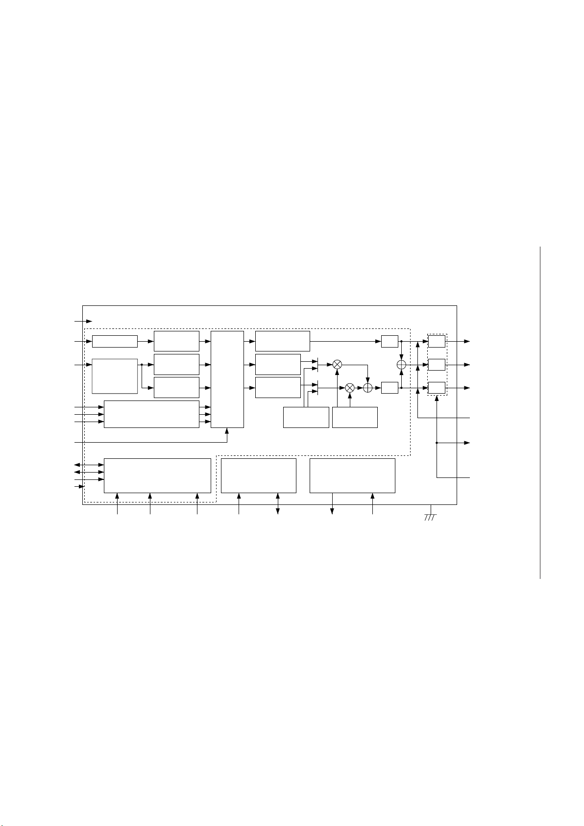
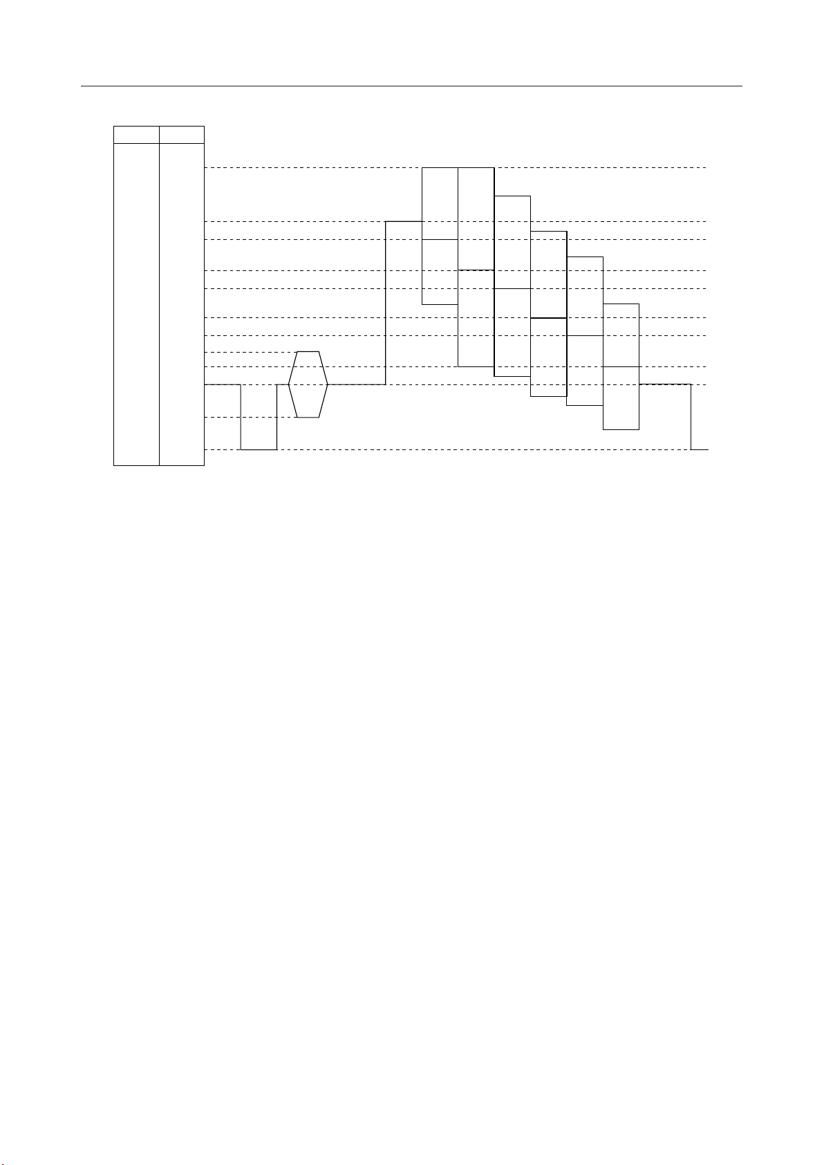
BLOCK DIAGRAM
Y Limitter
Y Level
Converter
Overlay
Control
Black &
Blank Pedestal
IPF
C Limitter
&
UV Selector
YD[7:0]
CD[7:0]
OLR
OLG
OLB
OLC
VSYNC_L
HSYNC_L
BLANK_L
CLKX1
U Level
Converter
Interpolator
+ LPF
V Level
Converter
Interpolator
+ LPF
YUV Color
generator
DAC
DAC
IPF DAC
Color Burst
Generator
Subcarrier
Generator
Sync Generator
&
Timing Controller
I2C Control Logic Test Control Logic
YA
CVBSO
CA
CT [8:0]
CLKX2O
RESET_L
TEST[4:1]TOUT[2:1]
SDASCLMODE[2:0]INTERLACEMS
CLKX2
X
Page 4
¡ Semiconductor MSM7650
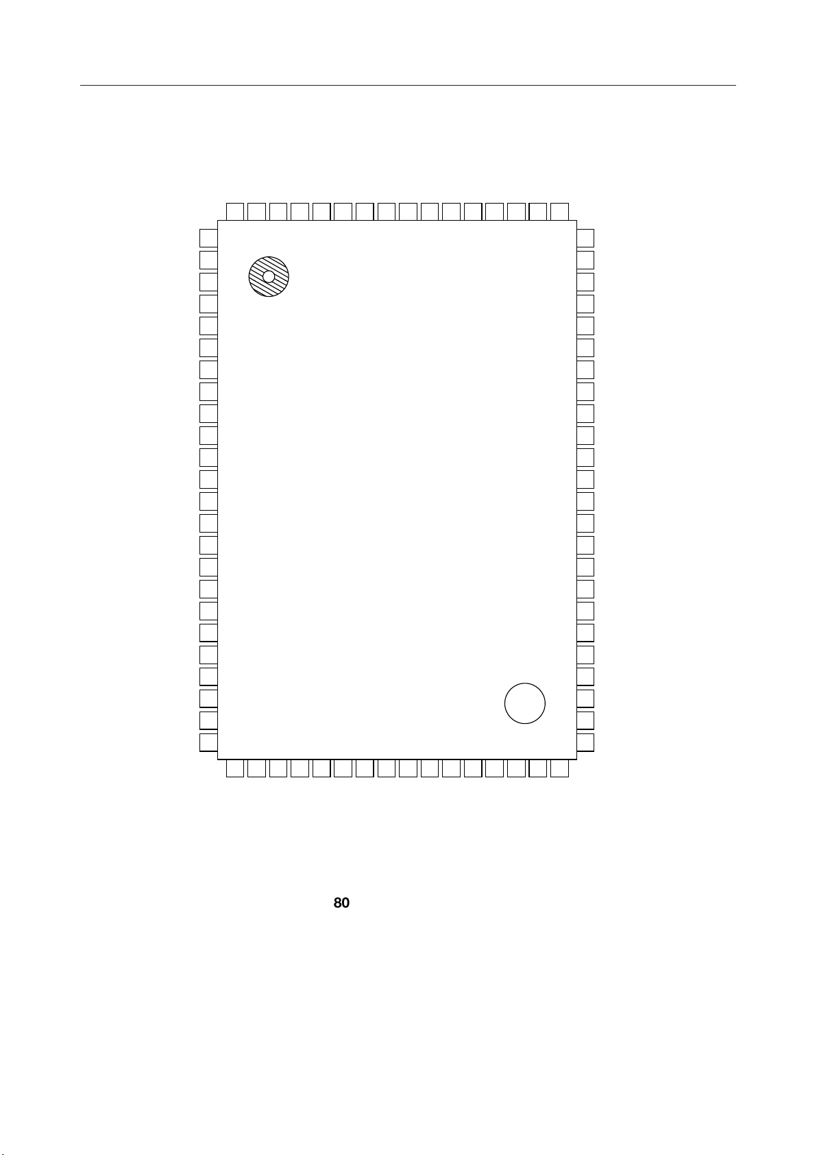
PIN CONFIGURATION (TOP VIEW)
CD7
CD6
CD5
CD4
CD3
CD2
CD1
CD0
YD7
YD6
YD5
YD4
YD3
YD2
YD1
YD0
806579
78
77
76
75
74
73
72
71
70
69
68
67
66
V
DD5
V
DD3
GND
VSYNC_L
HSYNC_L
BLANK_L
CLKX1
CLKX2
CLKX2O
X_L
V
DD3
GND
CT8
CT7
CT6
CT5
CT4
CT3
CT2
CT1
CT0
V
DD5
GND
1
2
3
4
5
6
7
8
9
10
X
11
MSM7650
12
13
14
15
16
17
18
19
20
21
22
23
24
64
V
63
V
62
GND
61
OLR
60
OLG
59
OLB
58
OLC
57
MODE[0]
56
MODE[1]
55
MODE[2]
54
INTERLACE
53
MS
52
RESET_L
51
SCL
50
SDA
49
ADRS
48
TOUT2
47
TOUT1
46
TEST4
45
TEST3
44
TEST2
43
TEST1
42
GND
41
V
DD5
DD3
DD3
254026
NC
DD3
V
27
VREF
28
29
30
31
32
FS
AGNDYAAGND
COMP
NC : No-connection pin
80-Pin Plastic QFP
33
DDAVDD
AV
34
35
36
AGND
CVBSO
37
CA
38
DD
AV
39
GND
NC
4/34
Page 5
¡ Semiconductor MSM7650
PIN DESCRIPTIONS (1/2)
Pin
1
2
3
4
5
6
7
8
9
10
11
12
13
14 to 22
23
24
25
26
27
28
29
30
31
32
33
34
35
36
37
38
39
40
41
42
43
44
45
I/O
I/O
I/O
I
I
I
O
I
O
I
I/O
I
I
I
O
O
O
I
I
Symbol
V
DD5
V
DD3
GND
VSYNC_L
HSYNC_L
BLANK_L
CLKX1
CLKX2
CLKX2O
X
X_L
V
DD3
GND
CT8 to CT0
V
DD5
GND
V
DD3
NC
VREF
FS
COMP
AGND
YA
AGND
AV
DD
AV
DD
CVBSO
AGND
CA
AV
DD
GND
NC
V
DD3
GND
TEST1
TEST2
TEST3
Description
5.0V power supply
3.3V power supply
Digital GND
Vertical sync signal
Polarity is negative. Output pin in master mode; input pin in slave mode.
Horizontal sync signal
Polarity is negative. Output pin in master mode; input pin in slave mode.
Composite blank signal. Polarity is negative.
Pixel clock input pin
Double pixel clock input pin
Double pixel clock output pin
Test pin. Normally, fixed to "0".
Test pin
3.3V power supply
Digital GND
Input pin for testing. Normally, fixed to "0" or "1".
5.0V power supply
Digital GND
3.3V power supply
Not connected
Reference voltage for DAC
DAC full scale adjustment pin
DAC phase compensation pin
Analog GND
Analog luminance signal output pin
Analog GND
Analog power supply
Analog power supply
Analog composite video signal output pin
Analog GND
Analog chrominance signal output pin
Analog power supply
Digital GND
Not connected
3.3V power supply
Digital GND
Input pin 1 for testing. Normally, fixed to "0".
Input pin 2 for testing. Normally, fixed to "0".
Input pin 3 for testing. Normally, fixed to "0".
5/34
Page 6
¡ Semiconductor MSM7650
PIN DESCRIPTIONS (2/2)
Pin
46
47
48
49
50
51
52
53
54
55 to 57
58
59
60
61
62
63
64
65 to 72
73 to 80
I/O
I
O
O
I
I/O
I
I
I
I
I
I
I
I
I
I
I
Symbol
TEST4
TOUT1
TOUT2
ADRS
SDA
SCL
RESET_L
MS
INTERLACE
MODE[2]
to MODE[0]
OLC
OLB
OLG
OLR
GND
V
DD3
V
DD5
YD0 to YD7
CD0 to CD7
Description
Input pin 4 for testing. Normally, fixed to "0".
Output pin for testing
Output pin for testing
2
C-bus subaddress setting pin. One of two addresses switchable can be
I
selected as subaddress.
1: 1000110/0: 1000100
2
I
C-bus data pin
2
I
C-bus clock pin
System reset pin. "1" at an open state by an internal pull-up resistor
Operation mode select signal pin for synchronization circuit.
1: master/0: slave. "1" at an open state by an internal pull-up resistor
Interlace/noninterlace select signal pin.
1: interlaced/0: noninterlaced. "1" at an open state by an internal pull-up
resistor
Video mode select pins
These pins are valid when MR[7] is "1".
000: NTSC CCIR
100: PAL CCIR
001: NTSC Square Pixel
101: PAL Square Pixel
010: NTSC 4Fsc
"000" at an open state by an internal pull-down resistor
Transparent control signal
Overlay signal is displayed when this pin is "H".
Overlay text color (Blue component)
Overlay text color (Green component)
Overlay text color (Red component)
Digital GND
3.3V power supply
5.0V power supply
Digital image luminance signal data input pin
Level is based on ITU-601. YD7 is MSB.
Digital image chrominance signal data input pin
Level is based on ITU-601. CD7 is MSB.
6/34
Page 7
¡ Semiconductor MSM7650
ABSOLUTE MAXIMUM RATINGS
Parameter
Power Supply Voltage
Input Voltage
Analog Output Current
Power Consumption
Storage Temperature
Symbol
V
DD5
V
DD3
AV
DD
V
I
I
O
P
W
T
STG
Condition
Ta=25°C
Ta=25°C
Ta=25°C
Ta=25°C
—
—
—
RECOMMENDED OPERATING CONDITIONS
Parameter
Power Supply Voltage
Power Supply Voltage
High Level Input Voltage
Symbol
V
DD5
V
DD3
AV
DD
GND
AGND
V
IH1
V
IH2
V
IH3
Condition
Ta=25˚C
Ta=25˚C
Ta=25˚C
Ta=25˚C
Ta=25˚C
SDA, CLKX1,
Except CLKX2,
Ta=25˚C
SDA, Ta=25˚C — V0.8
CLKX1,CLKX2,
Ta=25˚C
Min.
4.5
3.0
3.0
—
—
2.2
V
DD5
Rating
–0.3 to +7
–0.3 to +4.5
–0.3 to +4.5
–0.3 to V
800
–55 to +150
Typ.
5.0
3.3
3.3
0.0
0.0
40
—
—V2.4
DD5
+0.3
Max.
5.5
3.6
3.6
—
—
V
DD5
V
DD5
V
DD5
Unit
V
V
mA
mW
°C
Unit
V
V
V
Low Level Input Voltage
V
IL
Operating Temperature Range Ta — — ˚C
—
0.0
0.0
—
0.5
70
V
External Reference Voltage (*1) Vrefex — 1.25 V——
DA Current Setting Resistance (*2) Riadj — 330 W——
DA Output Load Resistance R
L
—75W——
(*1) When external reference voltage is not supplied, internal reference voltage is as
follows.
Internal Reference Voltage Vrefin — — V1.15 1.45
(*2) A volume control resistor of approx. 500W is recommendable for adjusting the output
current.
7/34
Page 8
¡ Semiconductor MSM7650
ELECTRICAL CHARACTERISTICS
DC Characteristics
(Ta=0 to +70°C, V
Parameter Symbol
High Level Output Voltage V
Low Level Output Voltage V
Input Leak Current I
Output Leak Current I
V
OH
OL
I
O
Condition
=–4mA (*1)
I
OH
I
=–8mA (*2)
OH
=4mA (*1)
I
OL
IOL=8mA (*2)
VI=GND to V
VI=GND to V
DD5
DD5
(*3)
Min.
0.8V
DD5
0
=3.3V±0.3V, V
DD3
Typ.
—
—V
— mA–10 10
— mA–10 10
DD5
Max.
V
DD5
0.6
=5V±10%)
Unit
CLKX1=13.5MHz
Power Supply Current (operating) I
DDO
CLKX2=27.0MHz
120 mA— 140
RESET_L="L"
Power Supply Current (standby) I
DDS
I2 C-bus SDA Output Voltage SDAV
I2C-bus SDA Output Current SDAI
CLKX1=CLKX2=0Hz
L
O
Low level, IOL=3mA
During Acknowledge
65 mA—80
—V0 0.4
—mA3—
Internal Reference Voltage Vrefin — — V1.15 1.45
DA Output Load Resistance R
L
—75W
Integral Linearity SINL ±2 LSB
Differential Linearity SDNL ±1 LSB
(*1) HSYNC_L, VSYNC_L, SDA, TO, CT[7:0]
(*2) CLKX2O
(*3) SDA
8/34
Page 9
¡ Semiconductor MSM7650
AC Characteristics
Parameter Symbol Condition Min. Typ. Max. Unit
CLKX Cycle Time T
Input Data Setup Time
Input Data Hold Time
Output Delay Time
CLKX2O Delay Time
Clock Cycle Time t
Clock Duty Cycle t
Low Level Cycle t
C_SCL
D_SCL
L_SCL
(Ta=0 to +70°C, V
PAL Square Pixel 67.8 ns
NTSC 4Fsc 69.8 ns
S
NTSC Square Pixel 81.5 ns
ITU-RS601 74.1 ns
t
s1
t
h1
t
d1
t
d2
—
—
—
—
=3.3V±0.3V, V
DD3
—
—
—
—
7.03 ns
9.48 ns
18.35 24.12 ns
7.69 9.53 ns
—
—
—
—
200
——
50 %
100
=5V±0.5V)
DD5
—
—
—
—
—
—
nsRpull_up=4.7kW
nsRpull_up=4.7kW
9/34
Page 10
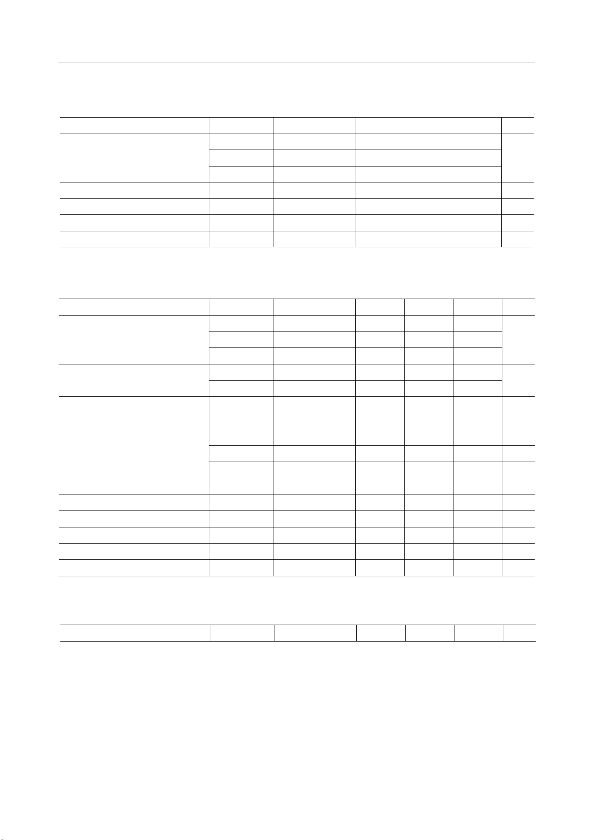
¡ Semiconductor MSM7650
CLKX1
t
s1
valid
invalid
t
h1
t
d1
Input timing
RESET_L, HSYNC_L, VSYNC_L,
YD[7:0], CD[7:0], MS, MODE[2:0],
INTERLACE, OLR, OLG, OLB,
OLC
Output timing
HSYNC_L, VSYNC_L
CLKX2
t
d2
CLKX2O
t
C_SCL
SCL
SDA
The phase relations between CLKX1 and CLKX2 are shown below.
1. When the CLKX1 pulse rises later than the CLKX2 pulse.
t
L_SCL
valid
CLKX2
Tccd1
CLKX1
2. When the CLKX1 pulse rises earlier than the CLKX2 pulse.
CLKX2
Tccd2
CLKX1
Tccd1: 20.14 [ns]
Tccd2: 3.27 [ns]
10/34
Page 11

¡ Semiconductor MSM7650
BLOCK FUNCTIONAL DESCRIPTION
Y Limitter
This block limits the contents outside the specified range as follows for input luminance signal
YD specified by the ITU-601 standard.
• Signals are limited to YD = 235 when YD_IN > 235
• Signals are limited to YD = 16 when YD_IN < 16
• In other cases, signals are fed as is to next processing
C Limitter
This block limits the contents outside the specified range as follows for input chrominance
signals specified by the ITU-601 standard.
The input chrominance signal is output as a 2’s complement format.
The processing procedure follows.
1) Format processing for input chrominance signals
• If MR [6] = 0, CD is in offset binary format. CD is converted to 2’s complement format and is
fed to next processing.
• If MR [6] = 1, CD is in 2’s complement format. CD is fed as is to next processing.
2) Clipping processing
• Signals are limited to CD = 112 when CD>112
• Signals are limited to CD = -112 when CD < -112
• In other cases, signals are fed to next processing
In addition, this block separates U and V components from the input chrominance signal CD into
which data of U and V components has been inserted using time sharing, and then passes signals
to the next process.
• Y Level Converter
Converts ITU-601 standard luminance signal level to DAC digital input level.
• U Level Converter
Converts ITU-601 standard chrominance signal level to DAC digital input level.
• V Level Converter
Converts ITU-601 standard chrominance signal level to DAC digital input level.
• YUV Color Generator
This block generates luminance and chrominance signals from over lay color signals OLR,
OLG and OLB. Control signals (CR [2:0] ) control the output content (overlay or color bar) and
output level (100%, 75%, 50%, 25%).
• Overlay Control
This block selects input image data or YUV Color Generator output signals.
It is determined by the level of the control signal (OLC, CR [2]), as shown below:
CR [2] = 1, OLC = ?: Selects color bar signal (YUV Color Generator output signal).
CR [2] = 0, OLC = 1: Selects overlay signal (YUV Color Generator output signal).
CR [2] = 0, OLC = 0: Selects input image data.
11/34
Page 12

¡ Semiconductor MSM7650
• Black & Blank Pedestal
This block adds sync signals at the luminance side to luminance signals.
• Interpolator +LPF
This block executes data interpolation and the elimination of high frequency components by
LPF for input chrominance signals. Both 4:2:2 and 4:1:1 signals are processed.
•I2C Control Logic
This is the serial interface block based on I2C standard of Phillips Corporation.
Internal registers MR and CR can be set from the master side.
When writing to the internal registers other than MR [5] (black level control) and CR [1:0]
(overlay level), written contents are immediately set to them. It is during the vertical blanking
period that written contents are set to MR [5] and CR [1:0].
• Sync Generator & Timing Controller
This block generates sync signals and control signals.
This block is operated in slave mode, which performs external synchronization, and in master
mode, which internally generates sync signals.
• Color Burst Generator
Outputs U and V components of amplitude of burst signals.
• Subcarrier Generator
Executes color subcarrier generation.
• Interpolation Filter (IPF)
This block performs upsampling at CLK X 2 (double speed CLKX1) for luminance signals and
chrominance signals modulated with CLKX1. Interpolation processing is executed in this
process.
12/34
Page 13

¡ Semiconductor MSM7650
INPUT DATA FORMAT
Input Digital Level
The content conforms to CCIR601 (ITU-601).
For chrominance input Cb and Cr, 2’s complement and offset binary formats are available by
setting of internal registers.
Input values outside the specified range are limited by internal clipping processing.
The valid input levels of luminance signal and chrominance signal are shown below.
Digital Level
100% White level
235
Black Level
16
Y data
Note) Values are in offset binary format.
(Values in parenthesis are in 2's complement format.)
Digital Level
240(112)
128(0)
16(–112)
C data
Input luminance signal level Input chrominance signal level
Basic Pixel Sampling Ratio
4:2:2 and 4:1:1 sampling are supported. An internal register can control the sampling ratio.
CLKX1
YD Y1 Y2 Y3 Y4 Y5 Y6
CD
U1 V1 U3 V3 U5 V5
4:2:2 sampling 4:1:1 sampling
CLKX1
YD Y1 Y2 Y3 Y4 Y5 Y6
CD
U1 V1 U5 V5
13/34
Page 14

¡ Semiconductor MSM7650
OUTPUT FORMAT
Output Level
When the output level of the operation mode is NTSC, the content of the output level differs
depending on setup level setting by internal registers.
When the setup level is set, data is output with Black-White as 92.5 IRE.
When the setup level is not set, data is output with Black-White as 100 IRE.
However, the setup level setting above is valid only when NTSC is selected as operation mode,
and setup level does not exist when PAL is selected as the operation mode.
When the contents of 100% luminance order color bar are input to the encoder, the DAC input
level is as follows.
DAC data Lumi [IRE]
480
389
359
307
276
227
197
169
144
135
114
59
133
100
89
70
59
41
30
20
11
7.5
0
–20
–40
4
Composite Wave Form (NTSC)
White
Yellow
Green
Cyan
NTSC composite signal (setup: 7.5 IRE)
Magenta
Red
Black
Blue
14/34
Page 15

¡ Semiconductor MSM7650
DAC data Lumi [IRE]
389
359
307
276
227
197
144
114
DAC data Lumi [IRE]
429
418
100
89
70
59
41
30
11
0
–40
4
63
59
Y Wave Form (NTSC)
NTSC Y signal output (setup: 0)
C Wave Form (NTSC)
Yellow
White
Yellow
Cyan
Cyan
Green
Green
Magenta
Magenta
Red
Red
Blue
Blue
Black
377
311
256
201
135
94
83
44
20
–20
–44
–59
–63
0
Color Burst
NTSC C signal output (setup: 0)
15/34
Page 16
¡ Semiconductor MSM7650
DAC data Lumi [IRE]
488
397
367
315
285
235
205
181
153
122
63
133
100
89
70
59
41
30
21.5
11
0
–21.5
–43
4
Composite Wave Form (PAL)
PAL composite signal
White
Yellow
Cyan
Green
Magenta
Red
Black
Blue
16/34
Page 17

¡ Semiconductor MSM7650
DAC data Lumi [IRE]
397
367
315
285
235
205
153
122
DAC data Lumi [IRE]
429
418
100
89
70
59
41
30
11
0
–43
4
63
59
Y Wave Form (PAL)
C Wave Form (PAL)
White
Yellow
Cyan
Green
PAL Y signal output
Yellow
Cyan
Green
Magenta
Magenta
Red
Red
Blue
Blue
Black
377
315
256
197
135
94
83
21.5
–21.5
–44
–59
–63
44
0
Color Burst
PAL C signal output
17/34
Page 18

¡ Semiconductor MSM7650
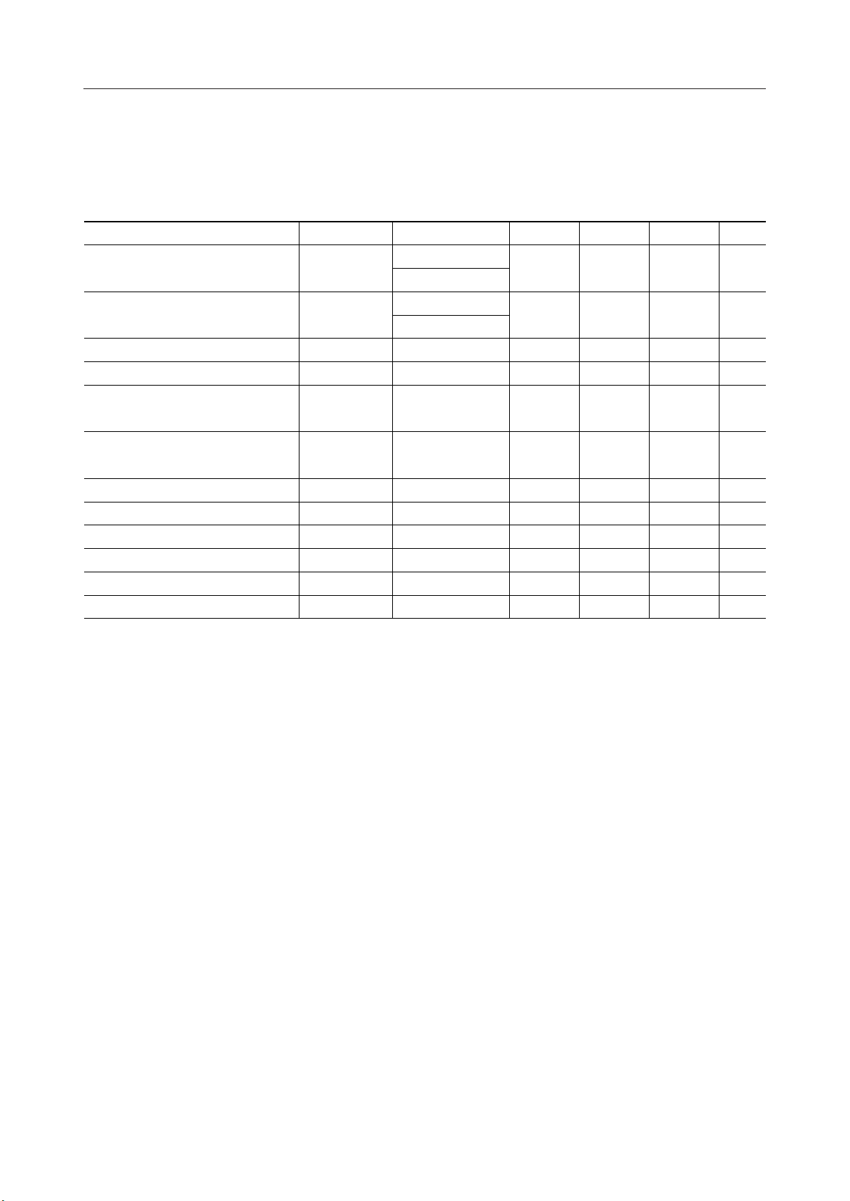
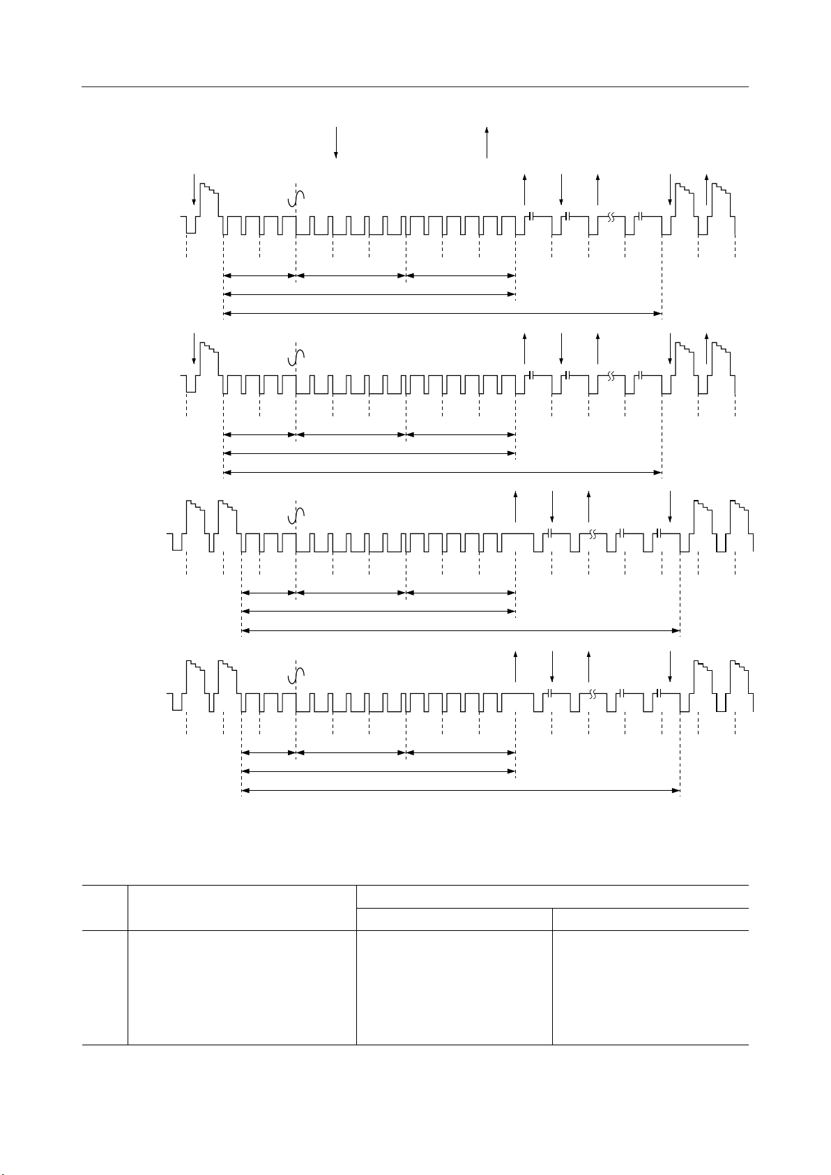
CLOCK TIMING
Input Data Timing
Input data and sync signals are fed into the encoder at the rising edge of the clock.
Input data is handled as valid pixel data when t
passes after the falling edge of HSYNC_L.
START
Chrominance signal of input data at this time is regarded as Cb.
ACTIVE VIDEO LINE
CLKX1
HSYNC_L
YD, CD
OLC, OLR
OLG, OLB
BLANK_L
t
START
t
s1
don't care don't care
t
ACT
t
h1
VALID DATA
Video data input timing
Input data is recognized as valid pixel data when input signal BLANK_L is high in the t
ACT
period.
When BLANK_L is high during the blanking period, however, input data is not output as valid
pixel data since processing to maintain blanking period is internally in-progress.
The values of t
follows.
In master mode
Operation mode
CCIR 601 NTSC
Square Pixel NTSC
4Fsc NTSC
CCIR PAL
Square Pixel PAL
t
STA–tS1=tSTART
differ slightly in master mode and slave mode. The values of t
START
In slave mode
t
STA
(Ts)
126
141
115
134
154
Operation mode
CCIR 601 NTSC
Square Pixel NTSC
4Fsc NTSC
CCIR PAL
Square Pixel PAL
t
STA
START
(Ts)
129
144
118
137
157
are as
18/34
Page 19

¡ Semiconductor MSM7650
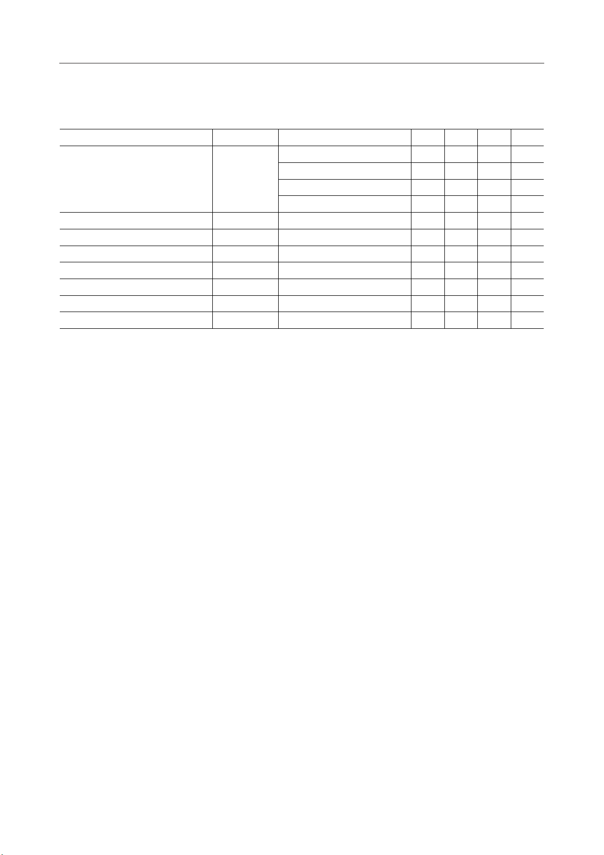
Internal Synchronization Output Timing
Input and output timing of HSYNC_L and VSYNC_L in master mode is as follows.
CLKX1
t
d1
HSYNC_L
VSYNC_L
Output timing of internal synchronization CLK1, HSYNC_L and VSYNC_L
VSYNC_L
t
d1
YA
5235245251234567 17 18
Output timing of internal synchronization VSYNC_L
19/34
Page 20

¡ Semiconductor MSM7650
Output Timing
Output timing conforms to CCIR Rep 624-4.
When the operation method is NTSC/PAL and the scanning method is interlace/noninterlace,
the output wave form content of composite signals are as follows.
Field 1
25926026126226312345678 171819
Field 2
25926026126226312345678 171819
Field 3
Reference sub-carrier phase
A B C
Reference sub-carrier phase
A B C
Reference sub-carrier phase
NEGATIVE HALF CYCLE
Burst relative 180° to B-Y axis
D
E
D
E
POSITIVE HALF CYCLE
Burst relative 180° to B-Y axis
25926026126226312345678 171819
A B C
D
E
Field 4
25926026126226312345678 171819
Reference sub-carrier phase
A B C
D
E
Output timing (interlaced NTSC)
20/34
Page 21

¡ Semiconductor MSM7650
Symbol
A
B
C
D
E
Name
First equalizing pulse period (3H)
Vertical synchronization period (3H)
Second equalizing pulse period (3H)
Burst pause period
Vertical blanking period (20H)
Output timing (interlaced NTSC)
Period
Odd field (Even field)
259.5 to 262.5H
1 to 3H
4 to 6H
1 to 6,259.5 to 262.5H
1 to 17,259.5 to 262.5H
21/34
Page 22
¡ Semiconductor MSM7650
Continuous Odd Field
Continuous Even Field
NEGATIVE HALF CYCLE
Burst relative 180° to B-Y axis
Reference sub-carrier phase
26026126212345678 171819
A B C
D
E
Reference sub-carrier phase
26026126212345678 171819
A B C
D
E
Reference sub-carrier phase
POSITIVE HALF CYCLE
Burst relative 180° to B-Y axis
Symbol
A
B
C
D
E
26026126212345678 171819
A B C
Reference sub-carrier phase
26026126212345678 171819
A B C
Output timing (noninterlaced NTSC)
Name
First equalizing pulse period (2H)
Vertical synchronization period (3H)
Second equalizing pulse period (2H)
Burst pause period
Vertical blanking period (19H)
D
E
D
E
Continuous odd field
261 to 262H
1 to 3H
4 to 6H
261 to 6H
261 to 17H
Period
Continuous even field
261.5 to 262H
1 to 3H
4 to 6H
261.5 to 6H
261.5 to 17.5H
Output timing (noninterlaced NTSC)
22/34
Page 23

¡ Semiconductor MSM7650
Field 1,5
Field 2,6
Field 3,7
burst phase +135°
+V
30931031131231312 345678 232425
A B C
D
E
30931031131231312 345678 232425
A B C
D
E
burst phase -135°
-V
Field 4,8
Symbol
A
B
C
D
E
30931031131231312 345678 232425
A B C
D
E
30931031131231312 345678 232425
A B C
D
E
Output timing (Interlaced PAL)
Name
First equalizing pulse period (2.5H)
Vertical synchronization period (2.5H)
Second equalizing pulse period (2.5H)
Burst pause period
Vertical blanking period (25H)
Filed 1,5
311 to 312.5H
1 to 2.5H
2.5 to 5H
1 to 6,310 to 312.5H
1 to 22.5,311 to 312.5H
Filed 2,6
311 to 312.5H
1 to 2.5H
2.5 to 5H
1 to 5.5,308.5 to 312.5H
1 to 22.5,311 to 312.5H
Period
Filed 3,7
311 to 312.5H
1 to 2.5H
2.5 to 5H
1 to 5,311 to 312.5H
1 to 22.5,311 to 312.5H
Filed 4,8
311 to 312.5H
1 to 2.5H
2.5 to 5H
1 to 6.5,309.5 to 312.5H
1 to 22.5,311 to 312.5H
Output timing (Interlaced PAL)
23/34
Page 24

¡ Semiconductor MSM7650
Continuous Odd Field
309
309
Continuous Even Field
burst phase +135°
+V
31031131212345678 232425
A B C
D
E
31031131212345678 232425
A B C
D
E
burst phase -135°
-V
Symbol
A
B
C
D
E
31031131212345678 232425
309
A B C
31031131212345678 232425
309
A B C
Output timing (Noninterlaced PAL)
Name
First equalizing pulse period (2H)
Vertical synchronization period (2.5H)
Second equalizing pulse period (2.5H)
Burst pause period
Vertical blanking period (24H)
D
E
D
E
Continuous odd field
311 to 312H
1 to 2.5H
2.5 to 5H
311 to 6H
311 to 22H
Period
Continuous even field
311.5 to 312H
1 to 2.5H
2.5 to 5H
311.5 to 6H
311.5 to 22.5H
Output timing (Noninterlaced PAL)
24/34
Page 25

¡ Semiconductor MSM7650
<Equalizing pulse vertical synchronization period>
Equalizing pulse vertical synchronization period
q
Setting content of equalizing pulse vertical
w
synchronization period (Ts is sampling clock cycle in each mode)
q w e
qEqualizing pulse width
wVertical sync pulse width
eSerration
qblanking level
w
(synchronizing+{blanking level) ¥ (2/3)
e
(synchronizing+{blanking level) ¥ (1/3)
rSynchronzing level
e
r
NTSC CCIR601
1/2H1/2H
PAL CCIR601
NTSC Square Pixel
NTSC 4Fsc
PAL Square Pixel
q
31Ts
32Ts
28Ts
33Ts
35Ts
w
398Ts
369Ts
332Ts
387Ts
403Ts
e
64Ts
63Ts
58Ts
68Ts
69Ts
1/2H
429Ts
432Ts
390Ts
455Ts
472Ts
Equalizing pulse vertical Equalizing pulse vertical
synchronization period synchronization period
<Horizontal blanking period>
1H
r
e
w
q
t
q w
e
r
t
qHorizontal sync pulse width
wBurst signal output period
eBurst signal start
rHorizontal blanking period (excluding front porch)
tFront porch start
qSynchronzing level
w
(synchronizing+{blanking level) ¥ (1/3)
e
(synchronizing+{blanking level) ¥ (2/3)
rblanking level
tpeak to peak value of burst
Horizontal blanking period
Setting content of horizontal blanking period (Ts is sampling clock cycle in each mode)
NTSC CCIR601
PAL CCIR601
NTSC Square Pixel
NTSC 4Fsc
PAL Square Pixel
q
63Ts
63Ts
58Ts
67Ts
69Ts
w
31Ts
31Ts
31Ts
36Ts
34Ts
e
71Ts
75Ts
65Ts
75Ts
82Ts
r
127Ts
142Ts
116Ts
135Ts
155Ts
t
838Ts
844Ts
762Ts
889Ts
922Ts
Total dots/1H
858
864
780
910
944
Setting content of horizontal blanking period
25/34
Page 26

¡ Semiconductor MSM7650
Internally Generated Color Bar Output Timing
This function outputs a 100% and 75% luminance order color bar by setting internal registers.
Output timing of each color of the color bar is as follows.
q
White Yellow Cyan Green
w
e
r
t
y
u
Magenta
Red Blue Black
Operation mode
NTSC CCIR601
NTSC Square Pixel
NTSC 4Fsc
PAL CCIR601
PAL Square Pixel
Each color of color bar output timing
hblank
127Ts
116Ts
135Ts
142Ts
155Ts
q
216Ts
197Ts
230Ts
230Ts
251Ts
w
305Ts
278Ts
325Ts
318Ts
347Ts
e
394Ts
359Ts
419Ts
406Ts
443Ts
r
483Ts
440Ts
513Ts
494Ts
539Ts
Each color of color bar output timing
t
572Ts
521Ts
607Ts
582Ts
635Ts
y
661Ts
602Ts
701Ts
670Ts
731Ts
(Ts is sampling clock cycle)
u
750Ts
682Ts
795Ts
757Ts
827Ts
1H
858Ts
780Ts
910Ts
864Ts
944Ts
26/34
Page 27

¡ Semiconductor MSM7650
I2C-bus Interface Input/Output Timing
Basic input/output timing of I2C-bus interface is shown below.
SDA
SCL
MSB
S
Start Condition
Data Line Stable: Data Valid Change of Data Allowed
12 789
I2C-bus basic input/output timing
ACK
t
C.SCL
12
t
L.SCL
3-8
9
ACK
P
Stop Condition
27/34
Page 28

¡ Semiconductor MSM7650
I2C BUS FORMAT
Basic input format of I2C-bus interface is shown below.
1 cycle
Slave AddressS Subaddress0A Data 0A A P
.....
Symbol
S
Slave Address
A
Subaddress
Data n
Slave AddressS Subaddress1A Data 1A A P
Description
Start condition
Slave address 1000100 or 1000000, 8th bit is write signal.
Acknowledge. Generated by slave
Subaddress byte
Data byte and acknowledge continues until data byte stop condition is met.
P Stop condition
It is required to input the above-mentioned format from the start condition to the stop condition
each time of writing a subaddress.
For example, when writing the subaddresses 0 to 2, the format should be input three times.
In case data of more than one byte are transferred,
Slave AddressS Subaddress0A Data 0A A P Data n A P
The 4th byte data and following data each are written over the same subaddress.
If one of the following matters occurs, the encoder will not return "A" (Acknowledge).
• The slave address does not match.
• A non-existent subaddress is specified.
• The read/write attribute of a register does not match "X" (read/write control bit).
The input timing is shown below.
SDA
SCL
S
Start Condition
2
18ACK
Slave Address
2
18ACK
Sub Address
2
18ACK
Data
P
Stop Condition
28/34
Page 29

¡ Semiconductor MSM7650
CONTENTS OF INTERNAL REGISTER SETTING
All registers can be written by accessing 8 bits.
"0" is read from an undefined bit.
The contents of internal registers are shown below. (A value with "*" is the default.)
Mode Register (MR) (Default value after system reset: 10H)
MR[7] Override Selects setting of external terminal or internal register
*0: setting of external terminal is valid
1: setting of internal registers is valid
MR[6] Chroma format Chrominance signal input format
*0: Offset binary
1: 2's Complement
MR[5] Black level control Black level setting (setup)
Note) Valid only for NTSC.
*0: Black level 7.5 IRE
1: Black level 0 IRE
MR[4] Synchronization mode Selects master/slave operation of sync signal generator.
0: slave mode
*1: master mode
MR[3] Pixel sampling ratio Sampling ratio
*0: 4:2:2
1: 4:1:1
MR[2:0] Video mode select Selects operation mode
*000: CCIR 601 NTSC 13.5 MHz
001: NTSC Square Pixel 12.27 MHz
010: NTSC 4Fsc 14.32 MHz
100: CCIR 601 PAL 13.5 MHz
101: PAL Square Pixel 14.75 MHz
29/34
Page 30

¡ Semiconductor MSM7650
Command Register (CR) (Default value after system reset: 1BH)
CR[7:5] Undefined Undefined
CR[4] Genlock Selects SCH phase management status
0: Genlock Off (subcarrier is self generated)
*1: Genlock On (management of SCH phase is
executed)
CR[3] Non-Interlace Scanning method in master mode
0: Non-Interlace
*1: Interlace
CR[2] Color bar Output control of luminance order color bar for
adjustment
*0: input image data or overlay data
1: luminance order color bar
CR[1:0] Overlay level Luminance signal output level control of overlay signals
and luminance order color bar for adjustment
00: 25%
01: 50%
10: 75%
*11: 100%
Data byte
D4
MR4
CR4
D3
MR3
CR3
D2
MR2
CR2
D1
MR1
CR1
D0
MR0
CR0
Mode Register (MR)
Command Register (CR)
SubaddressRegister function
0
1
D7
MR7
CR7
D6
MR6
CR6
D5
MR5
CR5
30/34
Page 31

¡ Semiconductor MSM7650
FILTER CHARACTERISTICS
The characteristics of LPF used for color signal processing and interpolation filters used for
upsampling processing are shown below.
LPF for 411 color signals
The following characteristics are when the clock frequency is 13.5 MHz.
0
–20
–40
Level [dB]
–60
–80
–100
01234567
Frequency [MHz]
411 Interpolation+LPF Frequency Characteristic
LPF for 422 color signals
The following characteristics are when the clock frequency is 13.5 MHz.
0
–20
–40
Level [dB]
–60
–80
–100
01234567
Frequency [MHz]
422 Interpolation + LPF Frequency Characteristic
31/34
Page 32
¡ Semiconductor MSM7650
Up Sampling Filter
The following characteristics are when the clock frequency is 27 MHz.
0
–20
–40
Level [dB]
–60
–80
–100
02468101214
Frequency [MHz]
Up Sampling Filter Frequency Characteristic
32/34
Page 33
¡ Semiconductor MSM7650
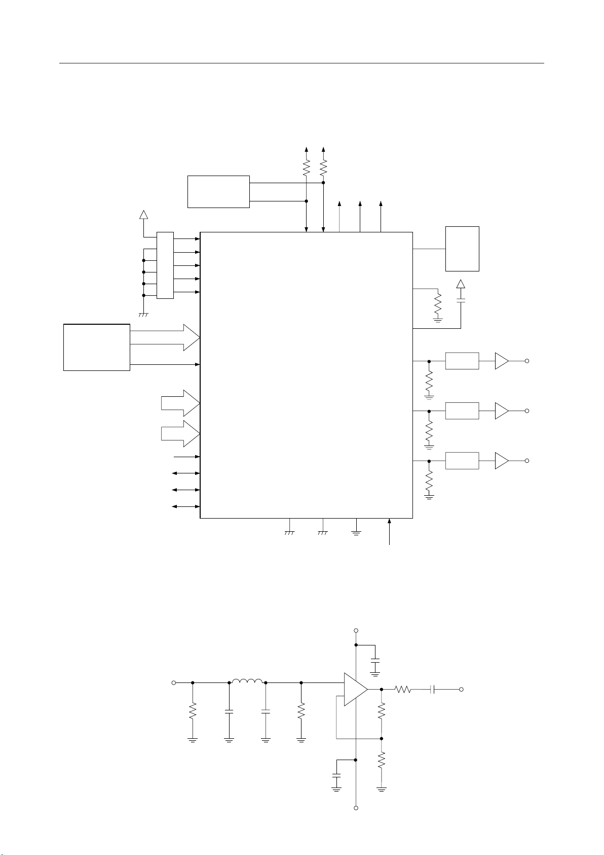
APPLICATION CIRCUIT EXAMPLE
5V5V
Overlay
Controller
DIP SW
I2C
Controller
MODE[2:0]
MS
INTERLACE
OLR
OLG
OLB
OLC
YD[7:0]YD[7:0]
CD[7:0]CD[7:0]
CLKX1
VSYNC_L
HSYNC_L
BLANK_L
R
I
SCL
MSM7650
GND AGND
X
R
5V
SDA
I
3.3V
3.3V
5
V
DD
3
V
DD
DD
AV
V
REF
External
reference
voltage
Typ. 1.25V
FS
C
R
C
C
COMP
LPF AMP
YA
R1
LPF AMP
CVBSO
R2
LPF AMP
CA
R2
CLKX2
Recommended Analog Output Circuit
YA, CA, CVBSO
150W
164pF
3.6mH
164pF
150W
0.1mF
+
–
+AVCC
–AVCC
0.1mF
75W
560W
560W
1000pF
+
OUTPUT
33/34
Page 34

¡ Semiconductor MSM7650
PACKAGE OUTLINES AND DIMENSIONS
25.0±0.2
20.0±0.2
^4 $1
$0
^5
1.0TYP.
14.0±0.2
19.0±0.2
INDEX MARK
Mirror finished surface
*0
0.8TYP.
0.17±0.05
q
2.1±0.2
2.5MAX.
0.05 to 0.35
0.8
0.12
2.5TYP.
0.25
0 to 10°
1.3TYP.
1.38±0.15
+0.08
0.32
–0.07
SEATING PLANE
@4
@5
0.16
M
34/34
 Loading...