

Page 1

E2U0037-28-82
¡ Semiconductor MSM7602
¡ Semiconductor
This version: Aug. 1998
Previous version: Nov. 1996
MSM7602
Echo Canceler
GENERAL DESCRIPTION
The MSM7602 is an improved version of the MSM7520 with the same basic configuration. The
MSM7602 uses a 19.2 MHz clock frequency to meet PHS, the 3 V power supply (2.7 V to 5.5 V),
and compact packaging. Also, this device adds the howling detecter control pins and main clook
output pins. (See the Appendix)
The MSM7602 is a low-power CMOS IC device for canceling echo (in an acoustic system or
telephone line) generated in a speech path.
Echo is canceled, in digital signal processing, by estimating the echo path and generating a
pseudo echo signal.
When used as an acoustic echo canceler, the device cancels the acoustic echo between the loud
speaker and the microphone which occurs during hands free communication such as with a
cellular phone or a conference system phone.
When used as a line echo canceler, the device cancels the line echo caused by impedance
mismatching in a hybrid.
In addition, the MSM7602 makes possible a quality conversation by controlling the noise level
and preventing howling with howling detector, double talk detector, attenuation function, and
a gain control function. The devise also controls the low level noise with a center clipping
function.
Further, the MSM7602 I/O interface supports m-law PCM . The use of a single chip CODEC, such
as the MSM7566/7704 (3 V) or MSM7543/7533 (5 V), allows an economic and efficient echo
canceler configuration.
FEATURES
• Handles both acoustic echoes and telephone line echoes.
• Cancelable echo delay time:
MSM7602-001 ................. For a single chip: 23 ms (max.)
MSM7602-011 ................. For a cascade connection (can also be used for a single chip)
Master chip: 23 ms (max.)
Slave chip: 31 ms (max.)
Cancelable up to 209 ms (1 master plus 6 slaves)
For a single chip: 23 ms (max.)
• Echo attenuation : 30 dB (typ.)
• Clock frequency : 19.2 MHz
External input and internal oscillator circuit are provided.
• Power supply voltage : 2.7 V to 5.5 V
• Package options:
28-pin plastic SSOP (SSOP28-P-485-0.65-K) (Product name : MSM7602-001GS-K)
56-pin plastic QFP (QFP56-P-910-0.65-2K) (Product name : MSM7602-011GS-2K)
1/29
Page 2
¡ Semiconductor MSM7602
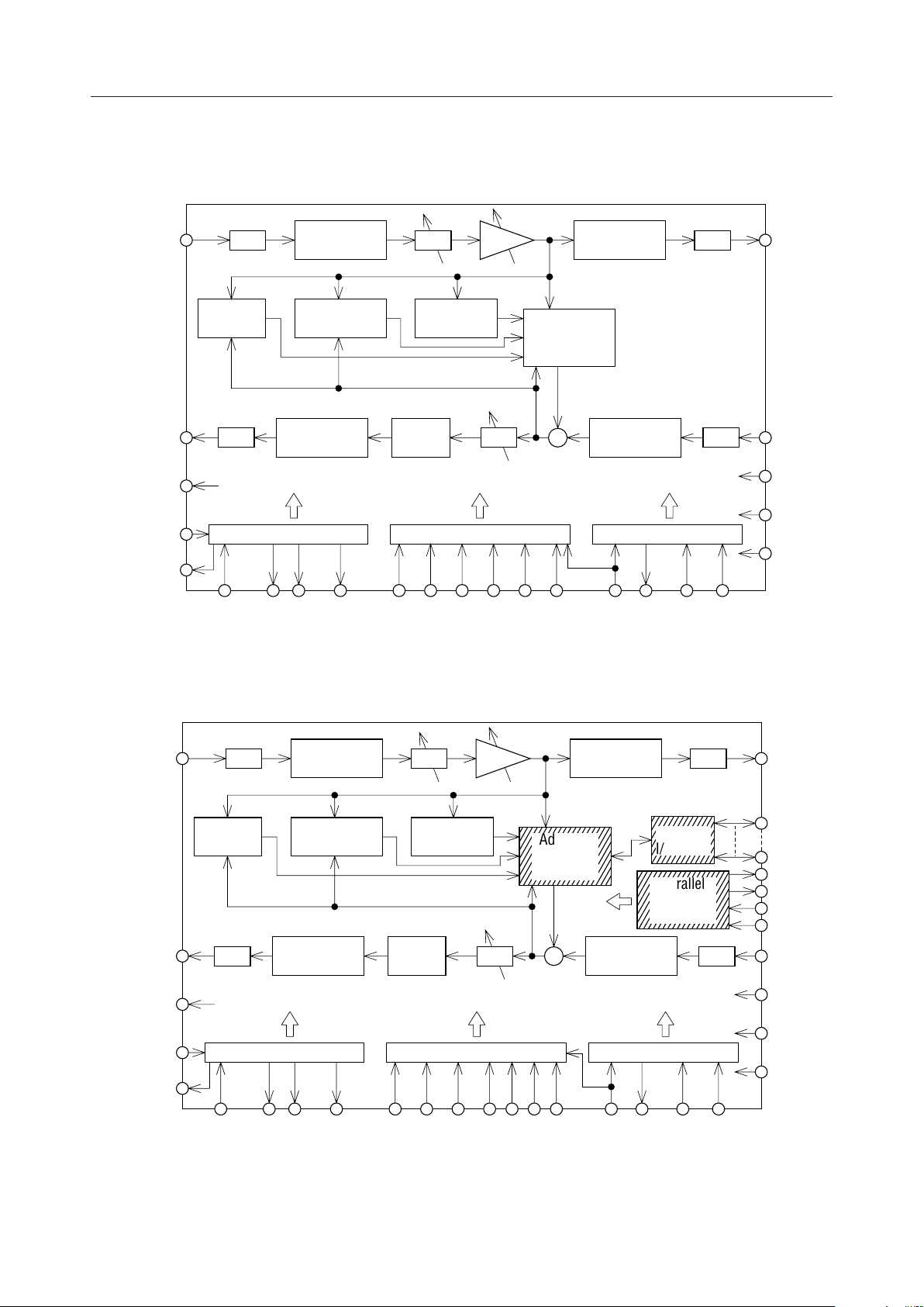
BLOCK DIAGRAM
MSM7602-001 (Single chip only)
RIN ROUT
S/P ATT Gain
Howling
Detector
Non–linear/
Linear
Double Talk
Detector
Power
Calculator
Linear/
Non–linear
Adaptive
FIR Filter
(AFF)
P/S
–
+
SOUT SIN
WDT
PWDWN
MCKO
P/S
*
Linear/
Non–linear
Clock Generator Mode Selector I/O Controller
Center
Clip
ATT
+
HD
Non–linear/
Linear
INT IRLD SCK SYNCNLP HCL ADP ATT GCSYNCOSCKOX2X1/CLKIN
S/P
RST
V
DD
V
SS
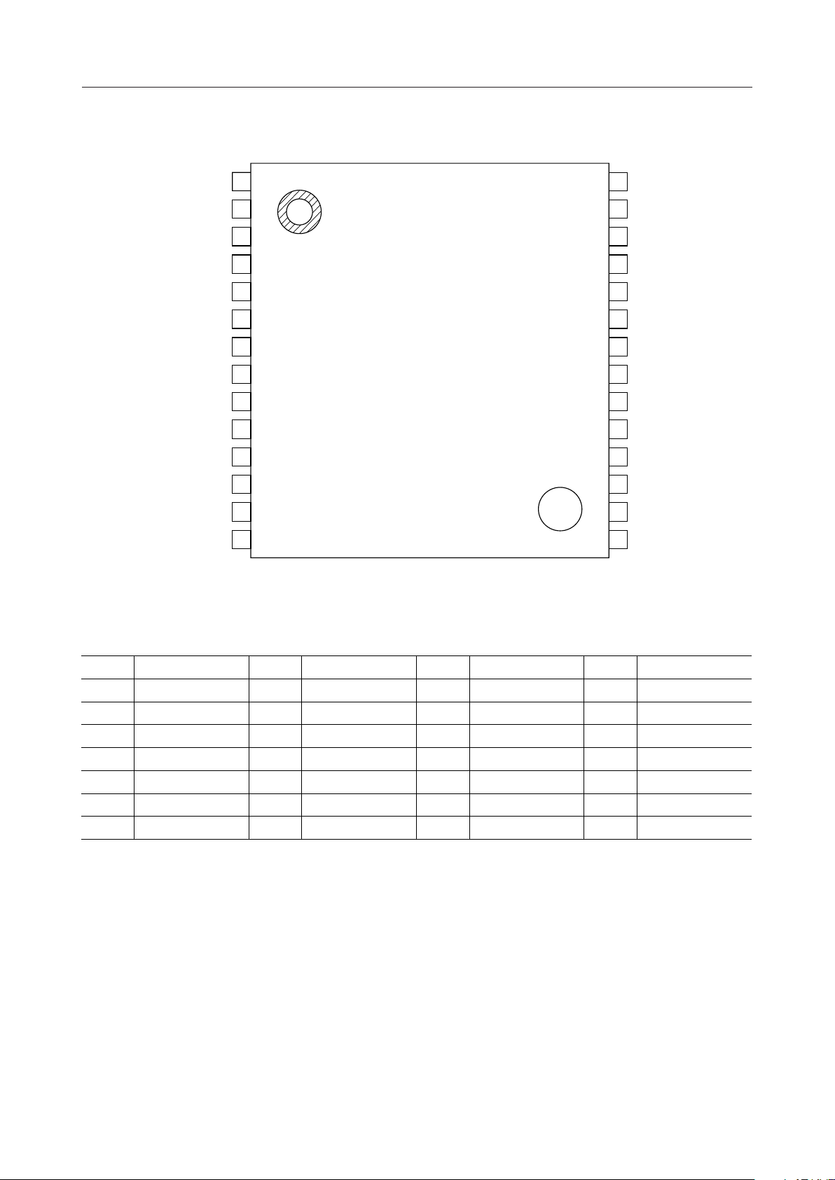
MSM7602-011 (Cascade connection or single chip)
RIN ROUT
SOUT SIN
WDT
* PWDWN
MCKO
* If the MSM7602-011 is used in the slave mode, only the diagonally hatched blocks and
the pins marked with * are used.
S/P ATT Gain
Howling
Detector
P/S
*
Clock Generator Mode Selector I/O Controller
*
Non–linear/
Linear
Double Talk
Detector
Linear/
Non–linear
Power
Calculator
Center
Clip
ATT
Adaptive
FIR Filter
(AFF)
–
+
+
MS
HD
*
Linear/
Non–linear
Non–linear/
Linear
INT *IRLD SCK SYNCNLP HCL *ADP ATT GCSYNCOSCKOX2X1/CLKIN
P/S
Parallel
I/O Port
Parallel
I/O
Controller
S/P
PD15
–
PD 0
OF1 *
OF2 *
SF1 *
SF2 *
RST *
VDD *
VSS *
*
*
2/29
Page 3
¡ Semiconductor MSM7602
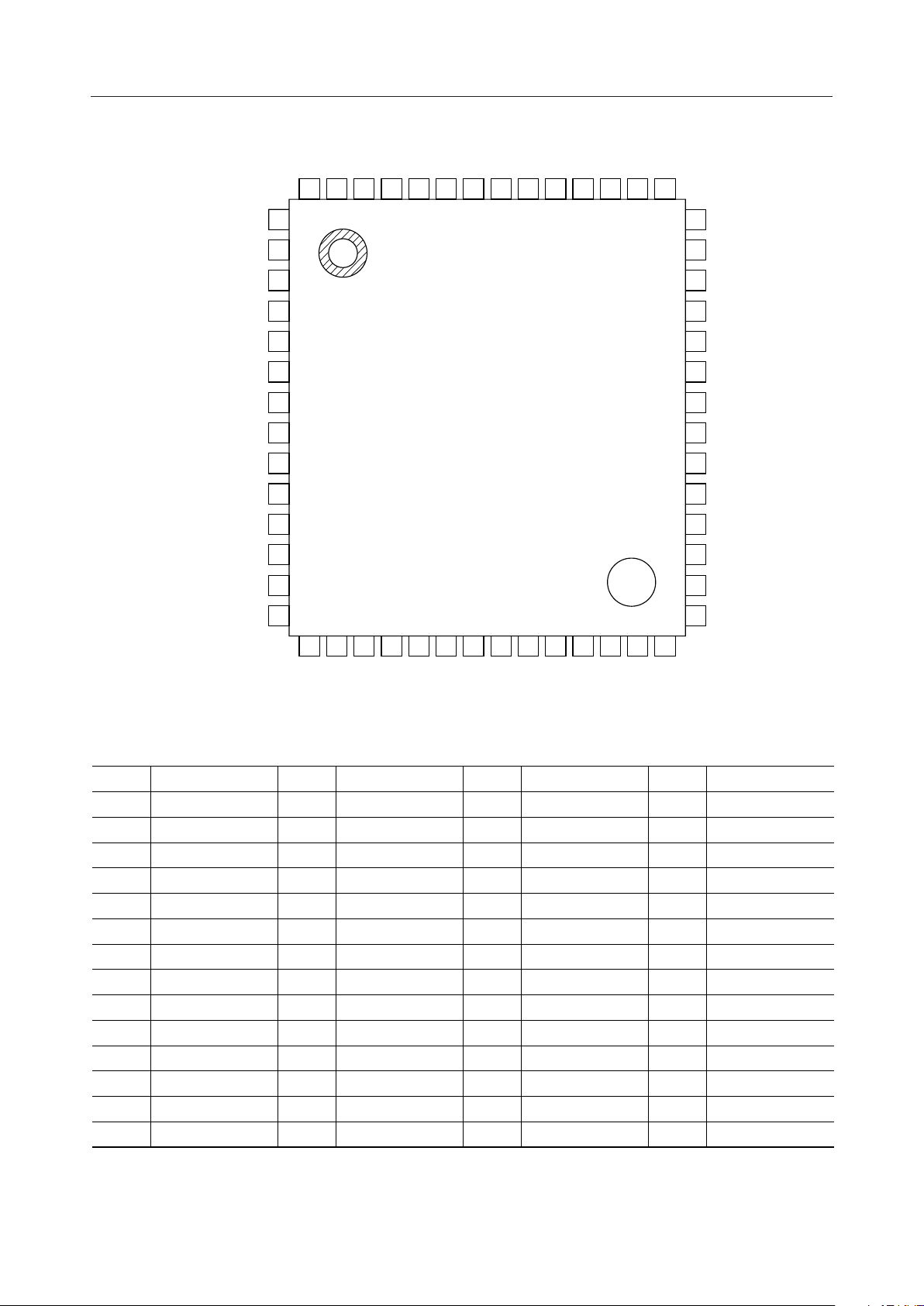
PIN CONFIGURATION (TOP VIEW)
10
11
12
13
14
1
2
3
4
5
6
7
8
9
28
27
26
25
24
23
22
21
20
19
18
17
16
15
28-Pin Plastic SSOP
Pin
1
2
3
4
5
6
7
Symbol
NLP
HCL
ADP
V
DD
ATT
INT
IRLD
Pin
8
9
10
11
12
13
14
Symbol
SIN
RIN
SCK
SYNC
SOUT
ROUT
V
SS
Pin
15
16
17
18
19
20
21
Symbol
V
SS
HD
X1/CLKIN
X2
V
DD
PWDWN
V
SS
Pin
22
23
24
25
26
27
28
Symbol
SYNCO
SCKO
RST
WDT
GC
V
DD
MCKO
3/29
Page 4
¡ Semiconductor MSM7602
56 4355 54 53 52 51 50 49 48 47 46 45 44
1
2
3
4
5
6
7
8
9
10
11
12
13
14
15 2816 17 18 19 20 21 22 23 24 25 26 27
42
41
40
39
38
37
36
35
34
33
32
31
30
29
56-Pin Plastic QFP
Pin
1
2
3
4
5
6
7
8 22 PD6 36
9 23 PD7 37
11 25 PD9 39
12 26 PD10 40 54 V
14 28 HD 42 V
Symbol
NLP
HCL
ADP
MS
ATT
INT
IRLD
Pin
15
16
17
18
19
20
21
Symbol
PD0
PD1
PD2
PD3
PD4
PD5
V
SS
Pin
29
30
31
32
33
34
35
SIN
RIN
SCK10 24 PD8 38
SYNC
SOUT
ROUT13 27 PD11 41 V
V
SS
Symbol
PD12
PD13
X1/CLKIN
X2
V
DD
PWDWN
V
SS
SYNCO
SCKO
RST
WDT
GC
DD
DD
Pin
43
44
45
46
47
48
49
50 *
51 V
52 SF1
53 OF2
55 V
56 *
*: No connect pin
Symbol
*
PD14
PD15
MCKO
SF2
OF1
V
SS
SS
DD
DD
4/29
Page 5

¡ Semiconductor MSM7602
PIN DESCRIPTIONS (1/5)
Pin
28-pin
SSOP
56-pin
QFP
1 1 NLP I
2 2 HCL I
3 3 ADP I
— 4 MS I
Symbol Type Description
Control pin for the center clipping function.
This pin forces the SOUT output to a minimum value when the SOUT
signal is below –54 dBm0. Effective for reducing low-level noise.
• Single Chip or Master Chip in a Cascade Connection
"H": Center clip ON
"L": Center clip OFF
• Slave Chip in a Cascade Connection
Fixed at "L"
This input signal is loaded in synchronization with the falling edge of the
INT signal or the rising edge of the RST signal.
Through mode control.
When this pin is in the through mode,
RIN and SIN data is output to ROUT and SOUT. At the same time, the
coefficient of the adaptive FIR filter is cleared.
• Single Chip or Master Chip in a Cascade Connection
"H": Through mode
"L": Normal mode (echo canceler operates)
• Slave Chip in a Cascade Connection
Same as master
This input signal is loaded in synchronization with the falling edge of the
INT signal or the rising edge of the RST signal.
AFF coefficient control.
This pin stops updating of the adaptive FIR filter (AFF) coefficient and sets
the coefficient to a fixed value, when this pin is configured to be the
coefficient fix mode.
This pin is used when holding the AFF coefficient which has been once
converged.
• Single Chip or Master Chip in a Cascade Connection
"H": Coefficient fix mode
"L": Normal mode (coefficient update)
• Slave Chip in a Cascade Connection
Fixed at "L"
This input signal is loaded in synchronization with the falling edge of the
INT signal or the rising edge of the RST signal.
Select signal.
This pin selects between the master chip and slave chip when
used in a cascade connection.
"L": Single chip or master chip
"H": Slave chip
5/29
Page 6

¡ Semiconductor MSM7602
(2/5)
Pin
28-pin
SSOP
56-pin
QFP
5 5 ATT I
Symbol Type Description
Control for the ATT function.
This pin prevents howling by attenuators (ATT) for the RIN input and SOUT
output.
If there is input only to RIN, the ATT for the SOUT output is activated.
If there is no input to SIN, or if there is input to both SIN and RIN, the ATT
for the RIN input is activated.
Either the ATT for the RIN output or the ATT for the SOUT is always
activated in all cases, and the attenuation of ATT is 6 dB.
• Single Chip or Master Chip in a Cascade Connection
"H": ATT OFF
"L": ATT ON
"L" is recommended if performing echo cancellation.
• Slave Chip in a Cascade Connection
Fixed at "L"
This input signal is loaded in synchronization with the falling edge of the
INT signal or the rising edge of the RST signal.
66 INT I
77 IRLD O
8 8 SIN I
9 9 RIN I
Interrupt signal which starts 1 cycle (8 kHz) of the signal processing.
Signal processing starts when "H"-to-"L" transition is detected.
• Single Chip or Master Chip in a Cascade Connection
Connect the IRLD pin.
• Slave Chip in a Cascade Connection
Connect the IRLD pin of the master chip.
INT input is invalid for 100 ms after reset due to initialization.
Refer to the control pin connection example.
Load detection signal output when the SIN and RIN serial input data is
loaded in the internal registers.
• Single Chip
Connect to the INT pin.
• Master Chip in a Cascade Connection
Connect to the INT pin of the master chip and all the slave chips.
• Slave Chip in a Cascade Connection Leave open.
Refer to the control pin connection example.
Transmit serial data.
Input the PCM signal synchronized to SYNC and SCK. Data is read in at
the falling edge of SCK.
Receive serial data.
Input the PCM signal synchronized to SYNC and SCK. Data is read at the
falling edge of SCK.
10 10 SCK I
Clock input for transmit/receive serial data.
This pin uses the external SCK or the SCKO.
Input the PCM CODEC transmit/receive clock (64 to 2048 kHz).
6/29
Page 7

¡ Semiconductor MSM7602
(3/5)
Pin
28-pin
SSOP
56-pin
QFP
11 11 SYNC I
Symbol Type Description
Sync signal for transmit/receive serial data.
This pin uses the external SYNC or SYNCO.
Input the PCM CODEC transmit/receive sync signal (8 kHz).
12 12 SOUT O
13 13 ROUT O
—
—
—
—
—
—
—
—
16 28 HD I
17 31 X1/CLKIN I
15
—
20
22
—
27
29
30
44
45
PD0
—
PD5
PD6
—
PD11
PD12
PD13
PD14
PD15
I/O
Transmit serial data.
Outputs the PCM signal synchronized to SYNC and SCK.
This pin is in a high impedance state during no data output.
Receive serial data.
Outputs the PCM signal synchronized to SYNC and SCK.
This pin is in a high impedance state during no data output.
This is the bidirectional bus pin for parallel data transfer between the
master chip and slave chip when used in a cascade connection.
The PD15 pin corresponds to MSB.
This pin is in a high impedance state during no data
output. Data is loaded in at the falling edge of SFx.
Controls the howling detect function.
generated during hand-free talking for acoustic system.
This function is used to cancel acoustic echoes.
• Single Chip or Master Chip in a Cascade Connection
"L": Howling detector ON
"H": Howling detector OFF
• Slave Chip in a Cascade Connection
Fixed at "L"
External input for the basic clock (17.5 to 20 MHz) or for the crystal
oscillator.
When the internal sync signal (SYNCO, SCKO) is used, input the basic
clock of 19.2 MHz.
This pin detets and cancels a howling
18 32 X2 O
Crystal oscillator output.
Used to configure the oscilation circuit.
Refer to the internal clock generator circuit example.
When inputting the basic clock externally, insert a 5 pF capacitor with
excellent high frequency characteristics between X2 and GND.
7/29
Page 8

¡ Semiconductor MSM7602
(4/5)
Pin
28-pin
SSOP
56-pin
QFP
20 34 PWDWN I
Symbol Type Description
Power-down mode control when powered down.
"L": Power-down mode
"H": Normal operation mode
During power-down mode, all input pins are disabled and output pins are
in the following states :
High impedance : SOUT, ROUT, PD0 to 15
"L": SYNCO, SCKO, MCKO
"H": OF1, OF2, X2
Holds the last state : WDT, IRLD
Reset after the power-down mode is released.
22 36 SYNCO O
23 37 SCKO O
24 38 RST I
25 39 WDT O
26 40 GC I
8 kHz sync signal for the PCM CODEC.
Connect to the SYNC pin and the PCM CODEC transmit/receive sync pin.
Leave it open if using an external SYNC.
Transmit clock signal (256 kHz) for the PCM CODEC.
Connect to the SCK pin and the PCM CODEC transmit/receive clock pin.
Leave it open if using an external SCK.
Reset signal.
"L": Reset mode
"H": Normal operation mode
Due to initialization, input signals are disabled for 100 ms after reset
(after RST is returned from L to H).
Input the basic clock during the reset.
Output pins during the reset are in the following states :
High impedance: SOUT, ROUT, PD0 to 15
"L": WDT
"H": OF1, OF2
Not affected: X2, SYNCO, SCKO, IRLD, MCKO
Test program end signal.
This signal is output when the one cycle (8kHz) of processing is completed.
Leave it open.
Input signal by which the gain controller for the RIN input is
controlled and the RIN input level is controlled and howling is
prevented.
The gain controller adjusts the RIN input level when it is –20 dBm0 or
above. RIN input levels from –20 to –11.5 dBm0 will be suppressed to
–20 dBm0 in the attenuation range from 0 to 8.5 dB.
RIN input levels above –11.5 dBm0 will always be attenuated by 8.5 dB.
• Single Chip or Master Chip in a Cascade Connection
"H": Gain control ON
"L": Gain control OFF
"H" is recommended for echo cancellation.
• Slave Chip in a Cascade Connection
Fixed at "L"
This pin is loaded in synchronization with the falling edge of the INT signal
or the rising edge of RST.
8/29
Page 9
¡ Semiconductor MSM7602
(5/5)
Pin
28-pin
SSOP
56-pin
QFP
Symbol Type Description
28 46 MCKO O
—47 SF2 I
—48 OF1 O
—52 SF1 I
Basic clock (19.2 MHz).
Parallel data transfer flag.
• Single Chip
Fixed at "H"
• Master Chip in a Cascade Connection
Fixed at "H"
• Slave Chip in a Cascade Connection
Connect OF2 of the master chip to the 1st stage slave chip.
Connect OF1 of the previous stage slave chip to the 2nd and later
stage slave chips.
Refer to the control pin connection example.
Parallel data transfer flag.
• Single Chip
Leave open.
• Master Chip in a Cascade Connection
Connect to the SF1 of all slaves.
• Slave chip in a Cascade Connection
Connect to the SF2 of the next stage slave chip.
Connect the last stage slave chip to the SF1 of the master chip.
Refer to the control pin connection example.
Parallel data transfer flag.
• Single Chip
Connect OF2.
• Master Chip in a Cascade Connection
Connect OF1 of the last stage slave chip.
• Slave Chip in a Cascade Connection
Connect OF1 of master chip for all slave chips.
Refer to the control pin connection example.
—53 OF2 O
Parallel data output flag.
• Single Chip
Connect to SF1.
• Master Chip in a Cascade Connection
Connect to SF2 of the 1st stage slave chip.
• Slave Chip in a Cascade Connection
Leave open.
Refer to the control pin connection example.
9/29
Page 10

¡ Semiconductor MSM7602
ABSOLUTE MAXIMUM RATINGS
Parameter
Power Supply Voltage
Input Voltage
Power Dissipation
Storage Temperature
Symbol
V
DD
V
IN
P
D
T
STG
Condition
Ta = 25˚C
—
RECOMMENDED OPERATING CONDITIONS
Parameter
Power Supply Voltage
Power Supply Voltage
High Level Input Voltage
Low Level Input Voltage
Operating Temperature
Parameter
Power Supply Voltage
Power Supply Voltage
High Level Input Voltage
Low Level Input Voltage
Operating Temperature
Symbol
V
DD
V
SS
V
IH
V
IL
Ta
Symbol
V
DD
V
SS
V
IH
V
IL
Ta
Condition
—
—
Pins other than X1
X1 pin 2.2 V—V
—
—
Condition
—
—
Pins other than X1, SCK
X1, SCK pins 3.5 V—V
—
—
Min.
2.7
—
2.0
0
–40
Min.
4.5
—
2.4
0
–40
Rating
–0.3 to +7
–0.3 to V
1
–55 to +150
Typ.
3.3
0
—
—
+25
Typ.
—
—
+25
Unit
+ 0.3
DD
(VDD = 2.7 V to 3.6 V)
Max.
Unit
3.6
—
V
DD
DD
0.5
+85
(VDD = 4.5 V to 5.5 V)
Max.
5
0
5.5
—
V
DD
DD
Unit
0.8
+85
V
V
W
˚C
V
V
V
V
˚C
V
V
V
V
˚C
ELECTRICAL CHARACTERISTICS
DC Characteristics
Parameter
High Level Output Voltage
Low Level Output Voltage
High Level Input Current
Low Level Input Current
High Level Output Leakage Current
Low Level Output Leakage Current
Power Supply Current (Operating)
Power Supply Current (Stand-by)
Input Capacitance
Output Load Capacitance
Symbol
V
OH
V
OL
I
IH
I
IL
I
OZH
I
OZLVOL
I
DDO
I
DDS
C
I
C
LOAD
IOH = 40 mA
I
OL
V
IH
MS with pull-down
V
IL
SF1, SF2
VOH = V
PWDWN = "L"
(VDD = 2.7 V to 3.6 V, Ta = –40˚C to +85˚C)
Condition Min. Typ. Max. Unit
2.2 — V
= 1.6 mA
= V
DD
0 — 0.4 V
— 0.1 1 mA
6 60 120 mA
= V
SS
with pull-up
DD
–1 –0.1 — mA
–60 –33 –6 mA
— 0.1 1 mA
PD15 to PD0
= V
SS
with pull-up
Input other than
the above
—
—
—
–60
–1
—
—
—
—
–33
–0.1
20
10
—
—
DD
–6
—
30
50
15
20
V
mA
mA
mA
mA
pF
pF
10/29
Page 11

¡ Semiconductor MSM7602
(V
= 4.5 V to 5.5 V, Ta = –40˚C to +85˚C)
DD
Typ.
—
—
0.1
100
–0.1
–50
0.1
–50
–0.1
30
10
—
—
Max. UnitParameter
V
DD
0.4 V
10 mA
200 mA
— mA
–10 mA
10 mA
–10
—
45
50
15
20
V
mA
mA
mA
mA
pF
pF
High Level Output Voltage
Low Level Output Voltage
High Level Input Current
Low Level Input Current
High Level Output Leakage Current
Low Level Output Leakage Current
Power Supply Current (Operating)
Input Capacitance
Input Capacitance
Output Load Capacitance
Symbol
V
OH
V
OL
I
IH
I
IL
I
OZH
I
OZL
I
DDO
I
DDS
C
I
C
LOAD
Condition Min.
= 40 mA
I
OH
IOL = 1.6 mA
V
= V
IH
DD
MS with pull-down
= V
V
IL
SS
SF1, SF2 with pull-up
VOH = V
DD
PD15 to PD0
VOL = V
SS
with pull-up
Input other than
the above
—
PWDWN = "L"
—
—
4.2
0
—
10
–10
–100
—
–100
–10
—
—
—
—
Echo Canceler Characteristics (Refer to Characteristics Diagram)
Parameter
Echo Attenuation
Cancelable Echo Delay Time for a
Single Chip or a Master Chip in a
Cascade
Cancelable Echo Delay Time for a
Slave Chip in a Cascade
Symbol
RES
T
D
T
DS
Condition Min. Typ. Max. Unit
RIN = –10 dBm0
(5 kHz band white noise)
E. R. L. (echo return loss)
= 6 dB
= 20 ms
T
D
ATT, GC, NLP: OFF
= –10 dBm0
R
IN
(5 kHz band white noise)
E. R. L. = 6 dB
ATT, GC, NLP: OFF
—30—dBL
— — 23 ms
— — 31 ms
11/29
Page 12

¡ Semiconductor MSM7602
AC Characteristics
(Ta = –40˚C to +85˚C)
V
= 2.7 V to 3.6 V VDD = 4.5 V to 5.5 V
Parameter
Symbol
Clock Frequency
f
When Internal Sync Signal is not used
C
Clock Cycle Time
t
When Internal Sync Signal is not used
Clock Duty Ratio
MCK
t
DMC
Clock "H" Level Pulse Width
t
fc = 19.2 MHz
MCH
Clock "L" Level Pulse Width
t
fc = 19.2 MHz
Clock Rise Time
Clock Fall Time
Sync Clock Output Time
Internal Sync Clock Frequency
Internal Sync Clock Output Cycle Time
Internal Sync Clock Duty Ratio
Internal Sync Signal Output Delay Time
Internal Sync Signal Period
Internal Sync Signal Output Width
Transmit/receive Operation Clock Frequency
Transmit/receive Sync Clock Cycle Time
Transmit/receive Sync Clock Duty Ratio
Transmit/receive Sync Signal Period
Sync Timing
Sync Signal Width
Receive Signal Setup Time
Receive Signal Hold Time t
Receive Data Input Time
IRLD Signal Output Delay Time
IRLD Signal Output Width
Serial Output Delay Time
Reset Signal Input Width
Reset Start Time t
Reset End Time t
Processing Operation Start Time t
MCL
t
t
t
DCM
f
CO
t
CO
t
DCO
t
DCC
t
CYO
t
WSO
f
SCK
t
SCK
t
DSC
t
CYC
t
XS
t
SX
t
WSY
t
DS
DH
t
t
DIC
t
WIR
t
SD
t
XD
t
WR
DRS
DRE
DIT
r
f
ID
DD
Min.
—
17.5
—
50
40
20.8
20.8
Typ.
19.2
—
52.08
—
—
—
—
Max.
—
20
—
57.14
60
31.3
31.3
—— 5
—— 5
——30
—
—
—
256
3.9
50
—
—
—
—— 5
—
—
64
0.488
40
123
125
t
CO
—
—
50
125
—
—
2048
15.6
60
—
45 — —
t
CYC-tSCK
—
t
45
SCK
—
—
45 — —
Min.
—
17.5
—
50
40
20.8
20.8
—
—
—
—
—
—
—
—
—
64
0.488
40
123
45
45
t
SCK
45
Typ.
19.2
—
52.08
—
—
—
—
—
—
—
256
3.9
50
—
125
t
CO
—
—
50
125
—
—
—
—
Max.
—
20
—
57.14
60
31.3
31.3
5
5
30
—
—
—
5
—
—
2048
15.6
60
—
—
t
CYC-tSCK
—
—
45 — — ns45 — —
—
7t
SCK
—
— — 138
—
—
—
1
5
—
t
SCK
—
—
—
—
—
—
90
90
—
—
52
—
—
—
—
—
7t
SCK
—
t
SCK
—
—
1
—
—
138
—
90
90
—
5——ns
— — 52 ns
100 — — 100 — — ms
Unit
MHz
ns
ns
ns
ns
ns
ns
ns
kHz
ms
%
ns
ms
ms
kHz
ms
%
ms
ns
ns
ms
ns
ms
ns
ms
ns
ns
ms
12/29
Page 13

¡ Semiconductor MSM7602
AC Characteristics (Continued)
(Ta = –40˚C to +85˚C)
V
= 2.7 V to 3.6 V VDD = 4.5 V to 5.5 V
Parameter
Power Down Start Time
Power Down End Time
Control Pin Setup Time (INT)
Control Pin Hold Time (INT)
Control Pin Setup Time (RST)t
Control Pin Hold Time (RST)t
Parallel Data Output Signal Width
Flag Signal Output Time
Flag Signal Output Width
Flag Signal Input Width
Data Read Setup Time
Data Read Hold Time
Symbol
t
DPS
t
DPE
t
DTS
t
DTH
DSR
DHR
t
WPD
t
DF
t
WFO
t
WFI
t
FS
f
FH
DD
Min.
— — 111
——15
20——
120 — —
20——
10——
—
——
—
—
—20—
—10—
Typ.
2t
MCK
t
MCK
t
MCK
t
WFO
/2
Max.
—
—
—
Min.
—
—
20
120
20——ns
10——ns
—
—
—
—
—
—
Typ.
—
—
—
—
2t
MCK
t
MCK
t
MCK
t
WFO
20
10
/2
Max.
111
15
—
—
—
—
—
—
—
—
Unit
ns
ns
ns
ns
ns
ns
ns
ns
ns
ns
13/29
Page 14

¡ Semiconductor MSM7602
TIMING DIAGRAM
Clock Timing
fC, t
MCK
X1/CLKIN
SCKO
fCO, t
SCKO
t
DCC
SYNCO
Serial Input Timing
t
WSO
CO
, t
DMC
t
DCC
t
DCM
t
DCO
t
t
CYO
MCH
t
MCL
t
DCM
t
r
t
f
SCK
SYNC
SIN
RIN
IRLD
f
, t
SCK
SCK
t
t
XS
SX
t
CYC
t
WSY
t
t
DS
DH
MSB
7
654321
t
ID
t
DIC
t
DSC
LSB
MSB
0
t
DIC
t
WIR
7
14/29
Page 15

¡ Semiconductor MSM7602
,
Serial Output Timing
f
SCK
SYNC
SOUT
ROUT
t
XS
t
High-Z
t
XD
SD
t
MSB
7
, t
SCK
SX
t
CYC
t
WSY
t
XD
654321
SCK
t
DSC
LSB
t
XD
High-Z
0
MSB
7
Operation Timing After Reset
t
WR
RST
t
DRS
Internal operaion
t
DRE
Reset Initialization
Power Down Timing
PWDWN
t
DPS
*Reset timing can be asynchronous
t
DIT
Processing Start
Note: INT is invalid in the diagonally shaded interval.
t
DPE
Internal Operation
Processing StartPower Down
15/29
Page 16

¡ Semiconductor MSM7602
Control Pin Load-in Timing
*t
CYC
INT(IRLD)
t
NLP, HCL, HD,
ATT, ADP, GC
RST
NLP, HCL, HD,
ATT, ADP, GC
t
t
DTS
DSR
t
WR
t
DHR
DTH
*For IRLD output timing, refer to Serial Input Timing
Parallel Output Timing
PD15
–
PD 0
OF1
OF2
High-Z High-Z
Parallel Input Timing
SF1
SF2
PD15
–
PD 0
t
WPD
Output Data
t
DF
t
FS
t
WFO
t
WFI
t
FH
Input Data
16/29
Page 17

¡ Semiconductor MSM7602
HOW TO USE THE MSM7602
The MSM7602 cancels (based on the RIN signal) the echo which returns to SIN.
Connect the base signal to the R side and the echo generated signal to the S side.
Connection Methods According to Echos
Example 1: Canceling acoustic echo (to handle acoustic echo from line input)
MSM7602
ROUT
RIN
Acoustic echo
+
AFF
–
SOUT
CODEC CODEC
SIN
H
+
Example 2: Canceling line echo (to handle line echo from microphone input)
Microphone input
CODEC CODEC
SOUT
RIN
MSM7602
AFF
–
+
+
ROUT
H
SIN
Line echo
Example 3: Canceling line echo in a cascade connection
(to handle line echo from microphone input)
Microphone input
RIN
MSM7602
Master
ROUT
Line input
CODEC CODEC
SOUT
AFF
–
+
Slave
AFF
+
SIN
PD0 - 15
H
Line echo
H
17/29
Page 18

¡ Semiconductor MSM7602
Example 4: Canceling of both acoustic echo and line echo
(to handle both acoustic echo from line input and line echo from microphone input)
MSM7602
ROUT
Acoustic echo
Microphone input
CODEC
SIN
AFF
+
For acoustic echo
Control Pin Connection Example
Single chip connection
HCL
ADP
ATT
GC
HD
PWDWN
RST
+5 V
MSM7602
RIN
SOUT
–
–
SOUT
RIN
AFF
SIN
+
+
CODEC
ROUT
Line input
H
+
Line echo
For line echo
MS *
NLPNLP
HCL
ADP
ATT
GC
HD
PWDWN
RST
INT
SF1 *
SF2 *
* PD15
–
* PD 0
IRLD
OF1
*
OF2
*
Asterisk (*) indicates a pin only for the MSM7602-011
2-stage cascade connection
Master + (slave ¥ 1)
HCL
ADP
ATT
GC
PWDWN
RST
+5 V
Master chip Slave chip
MS
PD15
NLPNLP
HCL
ADP
ATT
GC
HDHD
PWDWN
RST
INT
SF1
SF2
–
PD 0
IRLD
OF1
OF2
+5 V
MS
NLP
HCL
ADP
ATT
GC
HD
PWDWN
RST
INT
SF1
SF2
PD15
PD 0
IRLD
OF1
OF2
–
18/29
Page 19

¡ Semiconductor MSM7602
4-stage cascade connection
Master + (slave ¥ 3)
+5 V
MS
NLP
HCL
ADP
ATT
GC
PWDWN
RST
INT
SF1
SF2
HCL
ADP
ATT
GC
PWDWN
RST
+5 V
Master chip Slave chip 1
MS
PD15
NLPNLP
HCL
ADP
ATT
GC
HDHD HD HD HD
PWDWN
RST
INT
SF1
SF2
–
PD 0
IRLD
OF1
OF2
Internal Clock Generator Circuit Example
PD15
–
PD 0
IRLD
OF1
OF2
+5 V
Slave chip 2
MS
PD15
NLP
HCL
ADP
ATT
GC
PWDWN
RST
INT
SF1
SF2
–
PD 0
IRLD
OF1
OF2
+5 V
Slave chip 3
MS
PD15
NLP
HCL
ADP
ATT
GC
PWDWN
RST
INT
SF1
SF2
–
PD 0
IRLD
OF1
OF2
MSM7602
X1/CLKIN X2
R
C1 C2
GND GND
XTAL
External Clock Input Circuit Example
MSM7602
X1/CLKIN X2
CLK
5pF
XTAL
R
C1
C2
: 19.2 MHz
: 1 MW
: 27 pF
: 27 pF
GND
19/29
Page 20
¡ Semiconductor MSM7602
]
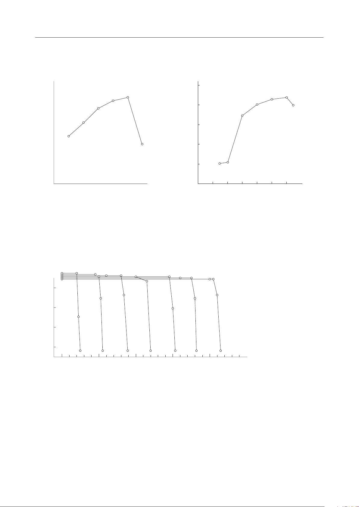
ECHO CANCELER CHARACTERISTICS DIAGRAM
ERL vs. echo attenuation
40
30
20
10
Echo attenuation [dB]
0
40 30 20 10 0
ERL [dB]
Measurement Conditions
RIN input = –10 dBm 5 kHz band white noise
(0 dBm = 2.2 dBm0)
Echo delay time T
ATT, GC, NLP = OFF
Power supply voltage 5 V
= 20 ms
D
–10
RIN input level vs. echo attenuation
40
30
20
10
Echo attenuation [dB]
0
–50 –40 –30 –20 –10 0
RIN input level [dBm]
0 dBm = 2.2 dBm0
Measurement Conditions
RIN input: 5 kHz band white noise
Echo delay time T
ERL = 6 dB
ATT, GC, NLP = OFF
Power supply voltage 5 V
= 20 ms
D
30
20
10
0
Echo attenuation [dB]
0
1 2 3 4 5 6 7chip
Echo delay time vs. echo attenuation
20015010050
Echo delay time [ms
Measurement Conditions
RIN input = –10 dBm
5 kHz band white noise
(0 dBm = 2.2 dBm0)
ERL = 6 dB
ATT, GC, NLP = OFF
The second through seventh chips
are connected in a cascade.
Power supply voltage 5 V
Note: The characteristics above are for the MSM7543 (VDD 5 V, m-law interface). The
MSM7566 (VDD 3 V, m-law interface) provides the same characleristics without input
and output levels. Refer to are PCM CODEC data sheet.
MSM7543 (for both transmit and receive)
0 dBm0 = 0.6007 Vrms = –2.2 dBm (600 W)
MSM7566 (for transmit side)
0 dBm0 = 0.35 Vrms = –6.9 dBm (600 W)
(for receive side)
0 dBm0 = 0.5 Vrms = –3.8 dBm (600 W)
20/29
Page 21

¡ Semiconductor MSM7602
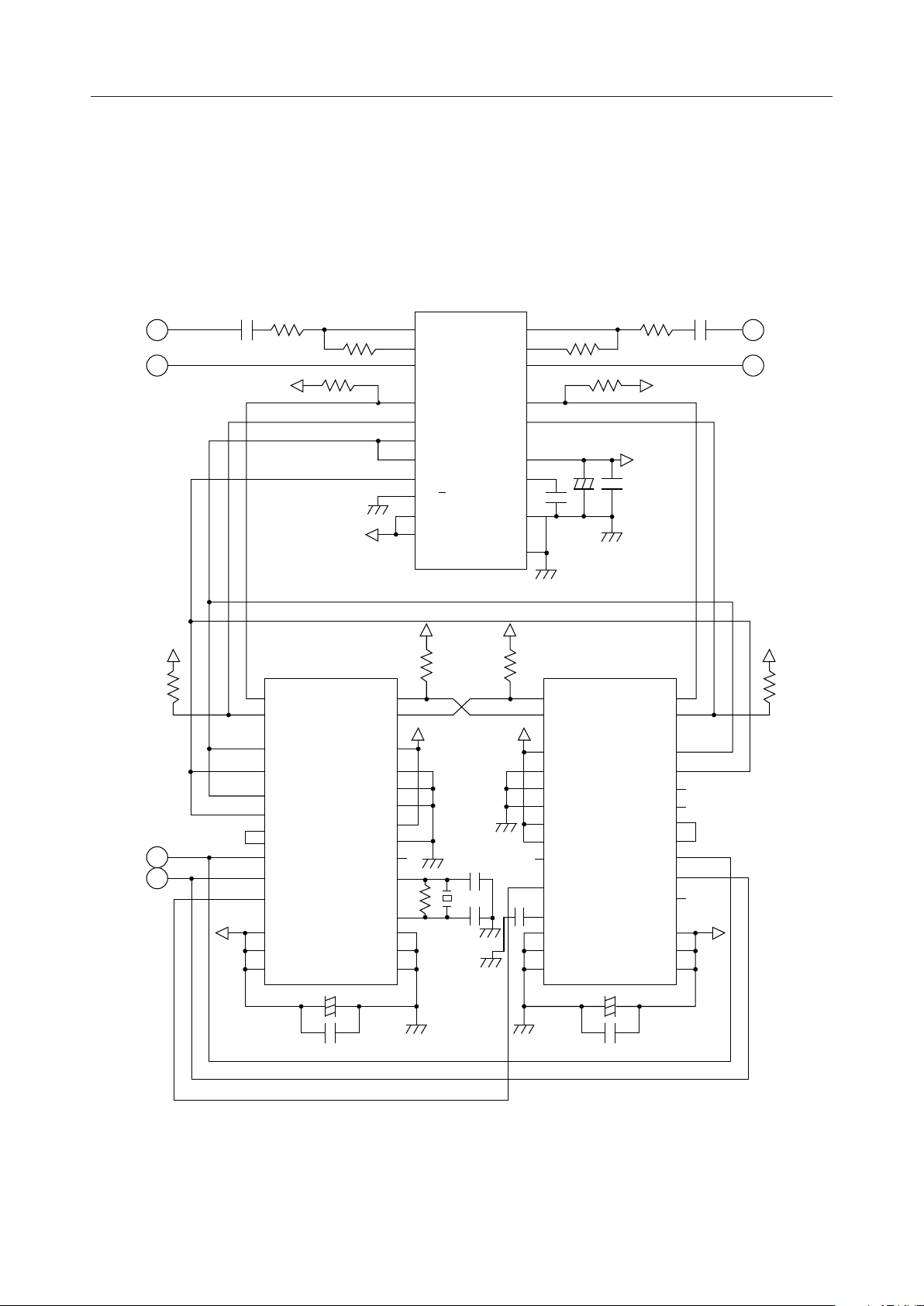
Measurement System Block Diagram
White noise generator
L. P. F.
5 kHz
Level meter
RIN
SOUT
MSM7543
AAPCM
m-law
CODEC
PCM
RIN
SOUT
Power supply voltage 5 V
ROUT
MSM7602
SIN
MSM7543
PCM
m-law
CODEC
PCMAA
T
D
Delay
Echo delay time
ATT
ERL
(echo return loss)
21/29
Page 22
¡ Semiconductor MSM7602
APPLICATION CIRCUIT
Bidirectional Connection Example
Microphone input
Speaker output
R4
PWDWN
RST
DV
C1 R1
DV
DV
For cancellation
of acoustic echo
MSM7602-001GS-K
8
SIN
13
ROUT
11
SYNC
10
SCK
22
SYNCO
23
SCKO
6
INT
7
IRLD
20
PWDWN
24
RST
28
MCKO
4
V
DD
19
V
DD
27
V
DD
+
Use the MSM7704-01GS-VK for PCM CODEC when V
The MSM7533 and MSM7704 are pin compatible.
2ch CODEC
MSM7533VGS-K
R3
DV
R2
21
22
4
13
12
15
10
16
19
5
6
AIN1
GSX1
AOUT1
DOUT1
DIN1
XSYNC
RSYNC
BCLK
A / m
PDN
CHP
DV
AOUT2
DOUT2
AIN2
GSX2
DIN2
V
DD
SGC
AG
DG
24
23
2
14
11
8
1
C9
18
9
For cancellation
R6
R7
+
C10 C11
of line echo
SOUT
RIN
R10DVR11
12
9
MSM7602-001GS-K
12
SOUT
9
RIN
DV DV
C14
26
16
25
17
18
14
15
21
1
2
3
5
NLP
HCL
ADP
ATT
GC
HD
WDT
X1
X2
V
SS
V
SS
V
SS
NLP
HCL
ADP
ATT
GC
HD
WDT
X1
X2
V
V
V
SS
SS
SS
1
2
3
5
26
16
25
17
R9
18
14
15
21
C12
C13
X1
C2
C3
C7
AV
(AG)
ROUT
SYNC
SCK
SYNCO
SCKO
IRLD
PWDWN
RST
+C6
DD
R5
SIN
INT
V
V
V
DD
DD
DD
3V.
DV
8
13
11
10
22
23
6
7
20
24
28
4
19
27
C5
Line input
Line output
DV
R8
DV
R1 = 20 kW
R2 = 20 kW
R3 = 2.2 kW
R4 = 10 kW
R10 = 10 kW
C1 = 1 mF
C2 = 10 mF
C3 = 0.1 mF
C4 = 0.1 mF
R5 = 20 kW
R6 = 20 kW
R7 = 2.2 kW
R8 = 10 kW
R11 = 10 kW
C5 = 1 mF
C6 = 10 mF
C7 = 0.1 mF
C8 = 0.1 mF
C9 = 0.1 mF
C10 = 10 mF
C11 = 0.1 mF
R9 = 1 MW
C12 = 27 pF
C13 = 27 pF
X1 = 19.2 MHz
C14 = 5 pF
22/29
Page 23

¡ Semiconductor MSM7602
Cascade Connection Example
When VDD is 3 V, use the MSM7566 for PCM CODEC.
RIN
The MSM7543 and MSM7566 are pin compatible.
SOUT
R9
R10
C5
23621
AIN+
VFRO
PCMOUT
PCMIN
MSM7543GS-VKMSM7543GS-VK Master
1312151114
8
131011
SIN
ROUT
Slave
SOUT
RIN
GSX
BCLOCK
SCK
PD15
R7
22
AIN
RSYNC
SYNC
PD14
R6
XSYNC
38
PD13
R8
1
SG
10
34
RST
PD12
3
AOUT–
PDM
TMC
19
PWDWN
PD11
PD10
5
PWI
1
NLP
PD 9
24
SGC
2
HCL
PD 8
C6
R13
+
C7
C10
8
16
DD
AG
V
DG
9
3
4
5
4028373631
GC
ATT
HD
SCKO
ADP
MS
MSM7602-011GS-2K
PD 7
PD 6
PD 5
PD 4
PD 3
PD 2
X1
SYNCO
PD 1
PD 0
12945443029272625242322201918171615534748
R7 > 20 kW
R8 > 20 kW
R9 = 2.2 kW
R10 = 10 kW
R12 = 0-22 W
R13 = 0-22 W
C6 = 10 mF
R1 > 50 kW
R2 > 20 kW
R3 > 20 kW
R4 = 2.2 kW
R5 = 10 kW
R6 > 50 kW
C1 = 0.1 mF
C13
C8
+
323341425554511421
DDVDDVDDVDDVDD
X2
V
OF2
SF2
OF1
SF1
INT
IRLD
6
7
52
463935
C7 = 0.1 mF
C8 = 10 mF
C2 = 10 mF
C3 = 0.1 mF
VSSVSSV
MCKO
WDT
C9 = 0.1 mF
C4 = 10 mF
VSSV
SS
49
C10 = 0.1 mF
C5 = 0.1 mF
SS
C13 = 5 pF
R11 = 1 MW
C11 = 27 pF
C12 = 27 pF
X1 = 19.2 MHz
12945443029272625242322201918171615534748526
SOUT
RIN
PD15
PD14
PD13
PD12
PD11
PD10
PD 9
PD 8
PD 7
PD 6
PD 5
PD 4
PD 3
PD 2
PD 1
PD 0
OF2
MSM7602-011GS-2K
SIN
ROUT
SCK
SYNC
RST
PWDWN
NLP
HCL
8
131011
R5
R4
1312151114
PCMIN
PCMOUT
AIN +
23621
C1
VFRO
RSYNC
BCLOCK
GSX
R2
XSYNC
AIN–
22
R1
38
R3
34
10
PDM
SG
1
AOUT–
5
3
1
PWI
ADPMSATTGCHD
2
3
19
TMC
SGC
8
24
C3
R12
4
5
9
DG
DD
AG
V
16
C9
+
C2
SCKO
SYNCOX1X2
4028373631
X1
C11
R11
C12
7
463935
SF2
INT
SF1
OF1
DDVDDVDDVDDVDDVSSVSSVSS
V
IRLD
MCKO
WDT
323341425554511421
+
C4
49
SSVSS
V
56-Pin QFP 56-Pin QFP
SIN
ROUT
RST
PWDWN
23/29
Page 24

¡ Semiconductor MSM7602
NOTES ON USE
1. Set echo return loss (ERL) to be attenuated. If the echo return loss is set to be
amplified, the echo can not be eliminated.
Refer to the characteristics diagram for ERL vs. echo attenuation quantity.
2. Set the level of the analog input so that the PCM CODEC does not overflow.
3. The recommended input level is –10 to –20 dBm0. Refer to the characteristics
diagram for the RIN input level vs. echo attenuation quantity.
4. Applying the tone signal to this echo canceler for long duration may decrease echo
attenuation.
When used with the HD pin "L" (howling detector ON), this echo canceler may
operate faultily if, while a signal is input to the RIN pin, a tone signal with a higher
level than the signal being input to RIN is input to the SIN pin.
A signal should therefore be input either to the RIN pin or to the SIN pin. If,
however, the tone signal is input to the SIN pin while a signal is input to the RIN pin,
the ADP, HD, or HCL pin must be set to "H".
5. For changes in the echo path (retransmit, circuit switching during transmission, and
so on), convergence may be difficult.
Perform a reset, to make it converge.
If the state of the echo path changes after a reset, convergence may again be difficult.
In cases such as a change in the echo path, perform a reset each time.
6. When turning the power ON, set the PWDWN pin to "1" and input the basic clock
simultaneously with power ON.
If powering down immediately after power ON, be sure fast input 10 or more clocks
of the basic clock.
7. After powering ON, be sure to reset.
8. After the power down mode is released (when the PWDWN pin is changed to "H"
from "L"), be sure to reset the device.
9. If this canceler is used to cancel acoustic echoes, an echo attenuation may be less
than 30 dB.
24/29
Page 25

¡ Semiconductor MSM7602
EXPLANATION OF TERMS
Attenuating Function : This function prevents howling and controls the noise level with
the attenuator for the RIN input and SOUT output. Refer to the
explanation of pins (ATT pin).
Echo Attenuation : If there is talking (input only to RIN) in the path of a rising echo
arises, the echo attenuation refers to the difference in the echo
return loss (canceled amount) when the echo canceler is not used
and when it is used.
Echo attenuation = (SOUT level during through mode operation)
– (SOUT level during echo canceler operation) [dB]
Echo Delay Time : This is the time from when the signal is output from ROUT until it
returns to SIN as an echo.
Acoustic Echo : When using a hands free phone, and so on, the signal output from
the speaker echoes and is input again to the microphone. The
return signal is referred to as acoustic echo.
Telephone Line Echo : This is a signal which is delayed midway in a telephone line and
returns as an echo, due to reasons such as a hybrid impedance
mismatch.
Gain Control Function : This function prevents howling and controls the sound level with
a gain controller for the RIN input. Refer to the explanation of pins
(GC pin).
Center Clipping Function : This function forces the SOUT output to a minimum value when
the signal is below –57 dBm0. Refer to the explanation of pins (NLP
pin).
Double Talk Detection : Double talk refers to a state in which the SIN and RIN signals are
input simultaneously. In a double talk state, a signal outside the
echo signal which is to be canceled can be input to the SIN input,
resulting in misoperation.
The double talk detector prevents such misoperation of the canceler.
Howling Detection : This is the oscillating state caused by the acoustic coupling between
the loud speaker and the microphone during hands free talking.
Howling not only interferes with talking, but can also cause in
misoperation of the echo canceler.
The howling detector prevents such misoperation and prevents
howling.
Echo Return Loss (ERL) : When the signal output from ROUT returns to SIN as an echo, ERL
refers to how much loss there is in the signal level during ROUT.
ERL = (ROUT level) – (SIN level of the ROUT signal which returns
as an echo) [dB]
If ERL is positive (ROUT > SIN), the system is an attenuator system.
If ERL is negative (ROUT < SIN), the system is an amplifier system.
PHS : Personal Handy Phone System.
25/29
Page 26

¡ Semiconductor MSM7602
APPENDIX Differences Between the MSM7602 and the MSM7520/7620
Introduction
The MSM7602 is the improved version of the MSM7520 with improved usage. Thus, there are no
differences in echo canceling characteristics.
Enhancements
• A new clock frequency of 19.2 MHz.
The basic clock frequency of the MSM7520/7620 was 18 or 38 MHz, while the basic clock
frequency of MSM7602 is 19.2 MHz. (MSM7602 can be applied at a frequency of 18 MHz.
However, external SYNC and SCK are required because the periods of SYNCO and SCKO are
varied.)
• Adoption of full-fledged 8-bit data through-mode
In the through-mode for the MSM7520 (HCL pin: "H"), an internally processed PCM signal was
used. Therefore, only the negative minimum value (7F
positive minimum value (FF
HEX
).
Analog to analog conversion causes no problem since both values are the minimum ones, but
data transfer in the through-mode encounters problems. Hence, in the MSM7620/7602, the
complete data trough-mode has been implemented.
) was converted into the corresponding
HEX
• Control of input timing to control pins (NLP, HCL, ADP, ATT and GC)
In MSM7520, asynchronous changes in a control pin may result in malfunctioning. This
problem stems from the fact that information on control pins is checked several times during
the execution of a program over one cycle and the state of a control pin is changed between the
first and second half periods.
The MSM7620/7602 provides an internal circuit for using an INT signal to hold control pin
information for one cycle. Thus, external timing control is not needed.
The howling detector control pin (HD) is added.
The MSM7602 can prevent the false detection of the howling detecter cause by tone signals by
providing the howling detecter control pins.
• Introduction of 256 kHz internal clock output (SCKO) for PCM transmission
Internal sync signals (SYNCO and SCKO) in MSM7520/7620 are rated at 8 kHz and 200 kHz,
respectively. At a frequency of 8 kHz, PCM multiplexing can be applied to no more than three
channels.
In the MSM7602, SCKO is rated at 256 kHz, while SYNCO at 8 kHz. Thus, PCM multiplexing
can be applied with up to four channels.
• Addition of basic clock output
The use of a crystal oscillator for a clock in the MSM7520/7620 requires an oscillating circuit
installed in each of two or more cascade-connected IC chips.
Since the MSM7602 supports basic clock output, only one IC chip requires an oscillating circuit.
(The MSM7602-001TS-K does not provide the basic clock output.)
26/29
Page 27

¡ Semiconductor MSM7602
• Small-sized package
MSM7602 Package code Package size (mm)
MSM7602-001GS-K :28-pin SSOP :SSOP28-P-485-0.65-K :9.5 ¥ 10.5 ¥ 1.85
MSM7602-011GS-2K :56-pin QFP :QFP56-P-910-0.65-2K :9.5 ¥ 10.5 ¥ 1.85
MSM7520 : 14.0 ¥ 14.0 ¥ 3.75 mm
MSM7620 : 14.0 ¥ 14.0 ¥ 2.1 mm
• Supply voltage rated at 3 volts
MSM7520/7620 4.5 V to 5.5 V 5 V typ.
MSM7602 2.7 V to 5.5 V 3.3 V or 5 V typ.
27/29
Page 28

¡ Semiconductor MSM7602
PACKAGE DIMENSIONS
(Unit : mm)
SSOP28-P-485-0.65-K
Mirror finish
Package material
Lead frame material
Pin treatment
Solder plate thickness
Package weight (g)
Epoxy resin
42 alloy
Solder plating
5 mm or more
0.39 TYP.
Notes for Mounting the Surface Mount Type Package
The SOP, QFP, TSOP, SOJ, QFJ (PLCC), SHP and BGA are surface mount type packages, which
are very susceptible to heat in reflow mounting and humidity absorbed in storage.
Therefore, before you perform reflow mounting, contact Oki’s responsible sales person for the
product name, package name, pin number, package code and desired mounting conditions
(reflow method, temperature and times).
28/29
Page 29

¡ Semiconductor MSM7602
(Unit : mm)
QFP56-P-910-0.65-2K
Mirror finish
Package material
Lead frame material
Pin treatment
Solder plate thickness
Package weight (g)
Epoxy resin
42 alloy
Solder plating
5 mm or more
0.43 TYP.
Notes for Mounting the Surface Mount Type Package
The SOP, QFP, TSOP, SOJ, QFJ (PLCC), SHP and BGA are surface mount type packages, which
are very susceptible to heat in reflow mounting and humidity absorbed in storage.
Therefore, before you perform reflow mounting, contact Oki’s responsible sales person for the
product name, package name, pin number, package code and desired mounting conditions
(reflow method, temperature and times).
29/29
 Loading...